

Page 1
500 MHz, Linear-in-dB VGA
V
V
FEATURES
Broad-range analog variable gain: −2.5 dB to +42.5 dB
3 dB cutoff frequency of 500 MHz
Gain up and gain down modes
Linear-in-dB, scaled 20 mV/dB
Resistive ground referenced input
Nominal Z
On-chip, square-law detector
Single-supply operation: 2.7 V to 5.5 V
APPLICATIONS
Cellular base stations
Broadband access
Power amplifier control loops
Complete, linear IF AGC amplifiers
High speed data I/O
GENERAL DESCRIPTION
= 200 Ω
IN
ICOM
INPT
ICOM
with AGC Detector
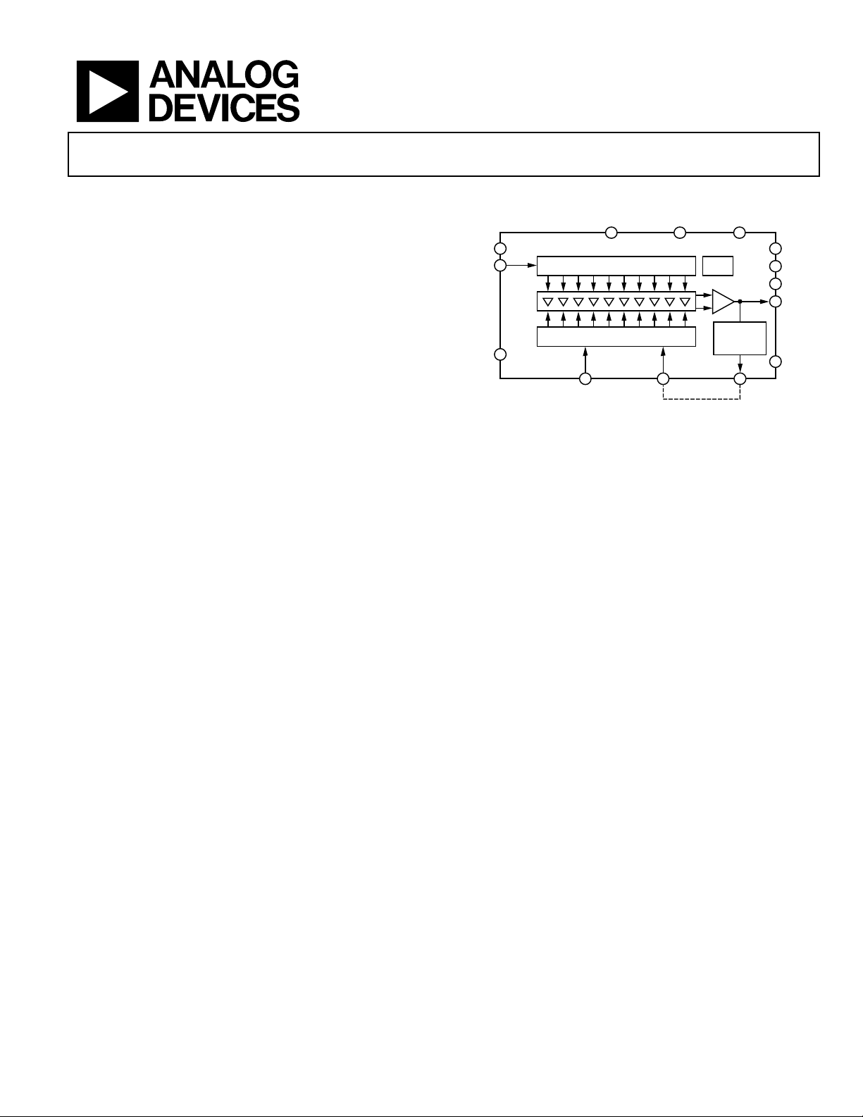
FUNCTIONAL BLOCK DIAGRAM
PSI
4
MODE
12
5
Figure 1.
1
3
CELLS
7
AD8367
9-STAGE ATTENUATOR BY 5dB
g
m
GAUSSIAN INTERPOLATOR
PSO
11
GAIN
AD8367
ENBL
2
BIAS
SQUARE
LAW
DETECTOR
6
DETO
14
13
10
9
8
ICOM
DECL
HPFL
VOUT
OCOM
02710-001
The AD8367 is a high performance 45 dB variable gain
amplifier with linear-in-dB gain control for use from low
frequencies up to several hundred megahertz. The range,
flatness, and accuracy of the gain response are achieved using
Analog Devices’ X-AMP® architecture, the most recent in a
series of powerful proprietary concepts for variable gain
applications, which far surpasses what can be achieved using
competing techniques.
The input is applied to a 9-stage, 200 Ω resistive ladder network.
Each stage has 5 dB of loss, giving a total attenuation of 45 dB.
At maximum gain, the first tap is selected; at progressively
lower gains, the tap moves smoothly and continuously toward
higher attenuation values. The attenuator is followed by a
42.5 dB fixed gain feedback amplifier—essentially an
operational amplifier with a gain bandwidth product of
100 GHz—and is very linear, even at high frequencies. The
output third order intercept is +20 dBV at 100 MHz (+27 dBm,
re 200 Ω), measured at an output level of 1 V p-p with V
= 5 V.
S
The analog gain-control input is scaled at 20 mV/dB and runs
from 50 mV to 950 mV. This corresponds to a gain of −2.5 dB
to +42.5 dB, respectively, when the gain up mode is selected and
+42.5 dB to −2.5 dB, respectively, when gain down mode is
selected. The gain down, or inverse, mode must be selected
when operating in AGC in which an integrated square-law
detector with an internal setpoint is used to level the output to
354 mV rms, regardless of the crest factor of the output signal.
A single external capacitor sets up the loop averaging time.
The AD8367 can be powered on or off by a voltage applied to
the ENBL pin. When this voltage is at a logic LO, the total
power dissipation drops to the milliwatt range. For a logic HI,
the chip powers up rapidly to its normal quiescent current of
26 mA at 25°C. The AD8367 is available in a 14-lead TSSOP
package for the industrial temperature range of −40°C to +85°C.
Rev. A
Information furnished by Analog Devices is believed to be accurate and reliable. However, no
responsibility is assumed by Anal og Devices for its use, nor for any infringements of patents or ot her
rights of third parties that may result from its use. Specifications subject to change without notice. No
license is granted by implication or otherwise under any patent or patent rights of Analog Devices.
Trademarks and registered trademarks are the property of their respective owners.
One Technology Way, P.O. Box 9106, Norwood, MA 02062-9106, U.S.A.
Tel: 781.329.4700 www.analog.com
Fax: 781.461.3113 © 2005 Analog Devices, Inc. All rights reserved.
Page 2

AD8367
TABLE OF CONTENTS
Features .............................................................................................. 1
Noise and Distortion.................................................................. 12
Applications....................................................................................... 1
Functional Block Diagram .............................................................. 1
General Description ......................................................................... 1
Revision History ............................................................................... 2
Specifications..................................................................................... 3
Absolute Maximum Ratings............................................................ 5
ESD Caution.................................................................................. 5
Pin Configuration and Function Descriptions............................. 6
Typical Performance Characteristics ............................................. 7
Theory of Operation ...................................................................... 11
Input Attenuator and Gain Control ......................................... 11
Input and Output Interfaces...................................................... 11
Power and Voltage Metrics........................................................ 12
REVISION HISTORY
Output Centering ....................................................................... 12
RMS Detection ........................................................................... 13
Applications..................................................................................... 14
Input and Output Matching ...................................................... 14
VGA Operation .......................................................................... 15
Modulated Gain Mode .............................................................. 15
AGC Operation .......................................................................... 15
Modifying the AGC Setpoint .................................................... 16
Evaluation Board ........................................................................ 19
Characterization Setup and Methods...................................... 20
Outline Dimensions ....................................................................... 21
Ordering Guide .......................................................................... 21
7/05—Rev. 0 to Rev. A
Changes to Format ............................................................. Universal
Changes to General Description .................................................... 1
Changes to Table 1............................................................................ 3
Changes to Table 3............................................................................ 6
Changes to Figure 8.......................................................................... 7
Changes to Figure 9, Figure 12, and Figure 14 ............................. 8
Changes to Input and Output Interfaces Section....................... 11
Changes to Output Centering Section and Figure 31................ 12
Changes to RMS Detection Section .............................................13
Changes to Figure 32, Table 4, and Table 5 ................................. 14
Changes to Figure 33, Figure 34, and
AGC Operation Section................................................................. 15
Changes to the Modifying the AGC Set Point Section.............. 16
Changes to Figure 38...................................................................... 17
Changes to Figure 42...................................................................... 19
Changes to Table 7.......................................................................... 20
Moved Table 7 to Page ................................................................... 20
Moved Characterization Setup and Methods Section to Page . 20
Moved Figure 45 to Page ............................................................... 20
Changes to Ordering Guide.......................................................... 21
Updated Outline Dimensions....................................................... 21
10/01—Revision 0: Initial Version
Rev. A | Page 2 of 24
Page 3

AD8367
SPECIFICATIONS
VS = 5 V, TA = 25°C, system impedance ZO = 200 Ω, V
Table 1.
Parameter Conditions Min Typ Max Unit
OVERALL FUNCTION
Frequency Range LF 500 MHz
GAIN Range 45 dB
INPUT STAGE Pins INPT and ICOM
Maximum Input To avoid input overload 700 mV p-p
Input Resistance From INPT to ICOM 175 200 225 Ω
GAIN CONTROL INTERFACE Pin GAIN
Scaling Factor V
V
= 5 V, 50 mV ≤ V
MODE
= 0 V, 50 mV ≤ V
MODE
Gain Law Conformance 100 mV ≤ V
Maximum Gain V
Minimum Gain V
V
Step Response From 0 dB to 30 dB 300 ns
GAIN
= 0.95 V +42.5 dB
GAIN
= 0.05 V −2.5 dB
GAIN
From 30 dB to 0 dB 300 ns
Small Signal Bandwidth V
= 0.5 V 5 MHz
GAIN
OUTPUT STAGE Pin VOUT
Maximum Output Voltage Swing RL = 1 kΩ 4.3 V p-p
R
= 200 Ω 3.5 V p-p
L
Output Source Resistance Series resistance of output buffer 50 Ω
Output Centering Voltage
1
V
SQUARE LAW DETECTOR Pin DETO
Output Set Point 354 mV rms
AGC Small Signal Response Time C
= 100 pF, 6 dB gain step 1 μs
AGC
POWER INTERFACE Pins VPSI, VPSO, ICOM, and OCOM
Supply Voltage 2.7 5.5 V
Total Supply Current
ENBL high, maximum gain, R
(includes load current)
Disable Current vs. Temperature ENBL low 1.3 1.6 mA
−40°C ≤ TA ≤ +85°C 1.8 mA
MODE CONTROL INTERFACE Pin MODE
Mode LO Threshold Device in negative slope mode of operation 1.2 V
Mode HI Threshold Device in positive slope mode of operation 1.4 V
ENABLE INTERFACE Pin ENBL
Enable Threshold 2.5 V
Enable Response Time
Time delay following LO to HI transition until
device meets full specifications.
Enable Input Bias Current ENBL at 5 V 27 μA
ENBL at 0 V 32 nA
f = 70 MHz
Gain Maximum gain +42.5 dB
Minimum gain −3.7 dB
Gain Scaling Factor 19.9 mV/dB
Gain Intercept −5.6 dB
Noise Figure Maximum gain 6.2 dB
Output IP3 f1 = 70 MHz, f2 = 71 MHz, V
29.5 dBV rms
Output 1 dB Compression Point V
= 0.5 V 8.5 dBm
GAIN
1.5 dBV rms
= 5 V, f = 10 MHz, unless otherwise noted.
MODE
≤ 950 mV +20 mV/dB
GAIN
≤ 950 mV −20 mV/dB
GAIN
≤ 900 mV ±0.2 dB
GAIN
/2 V
S
= 200 Ω
L
26 30 mA
1.5 μs
= 0.5 V 36.5 dBm
GAIN
Rev. A | Page 3 of 24
Page 4

AD8367
Parameter Conditions Min Typ Max Unit
f = 140 MHz
Gain Maximum gain +43.5 dB
Minimum gain −3.6 dB
Gain Scaling Factor 19.7 mV/dB
Gain Intercept −5.3 dB
Noise Figure Maximum gain 7.4 dB
Output IP3 f1 = 140 MHz, f2 = 141 MHz, V
25.7 dBV rms
Output 1 dB Compression Point V
= 0.5 V 8.4 dBm
GAIN
1.4 dBV rms
f = 190 MHz
Gain Maximum gain +43.5 dB
Minimum gain −3.8 dB
Gain Scaling Factor 19.6 mV/dB
Gain Intercept −5.3 dB
Noise Figure Maximum gain 7.5 dB
Output IP3 f1 = 190 MHz, f2 = 191 MHz, V
23.9 dBV rms
Output 1 dB Compression Point V
= 0.5 V 8.4 dBm
GAIN
1.4 dBV rms
f = 240 MHz
Gain Maximum gain +43 dB
Minimum gain −4.1 dB
Gain Scaling Factor 19.7 mV/dB
Gain Intercept −5.2 dB
Noise Figure Maximum gain 7.6 dB
Output IP3 f1 = 240 MHz, f2 = 241 MHz, V
22.2 dBV rms
Output 1 dB Compression Point V
= 0.5 V 8.1 dBm
GAIN
1.1 dBV rms
1
The output dc centering voltage is normally set at VS/2 and can be adjusted by applying a voltage to DECL.
= 0.5 V 32.7 dBm
GAIN
= 0.5 V 30.9 dBm
GAIN
= 0.5 V 29.2 dBm
GAIN
Rev. A | Page 4 of 24
Page 5
AD8367
ABSOLUTE MAXIMUM RATINGS
Table 2.
Parameter Rating
Supply Voltage VPSO, VPSI 5.5 V
ENBL Voltage VS + 200 mV
MODE Select Voltage VS + 200 mV
V
Control Voltage 1.2 V
GAIN
Input Voltage ±600 mV
Internal Power Dissipation 250 mW
θ
JA
Maximum Junction Temperature 125°C
Operating Temperature Range −40°C to +85°C
Storage Temperature Range −65°C to +150°C
Lead Temperature Range
(Soldering 60 sec)
150°C/W
300°C
ESD CAUTION
ESD (electrostatic discharge) sensitive device. Electrostatic charges as high as 4000 V readily accumulate
on the human body and test equipment and can discharge without detection. Although this product features
proprietary ESD protection circuitry, permanent damage may occur on devices subjected to high energy
electrostatic discharges. Therefore, proper ESD precautions are recommended to avoid performance
degradation or loss of functionality.
Stresses above those listed under Absolute Maximum Ratings
may cause permanent damage to the device. This is a stress
rating only; functional operation of the device at these or any
other conditions above those indicated in the operational
section of this specification is not implied. Exposure to absolute
maximum rating conditions for extended periods may affect
device reliability.
Rev. A | Page 5 of 24
Page 6
AD8367
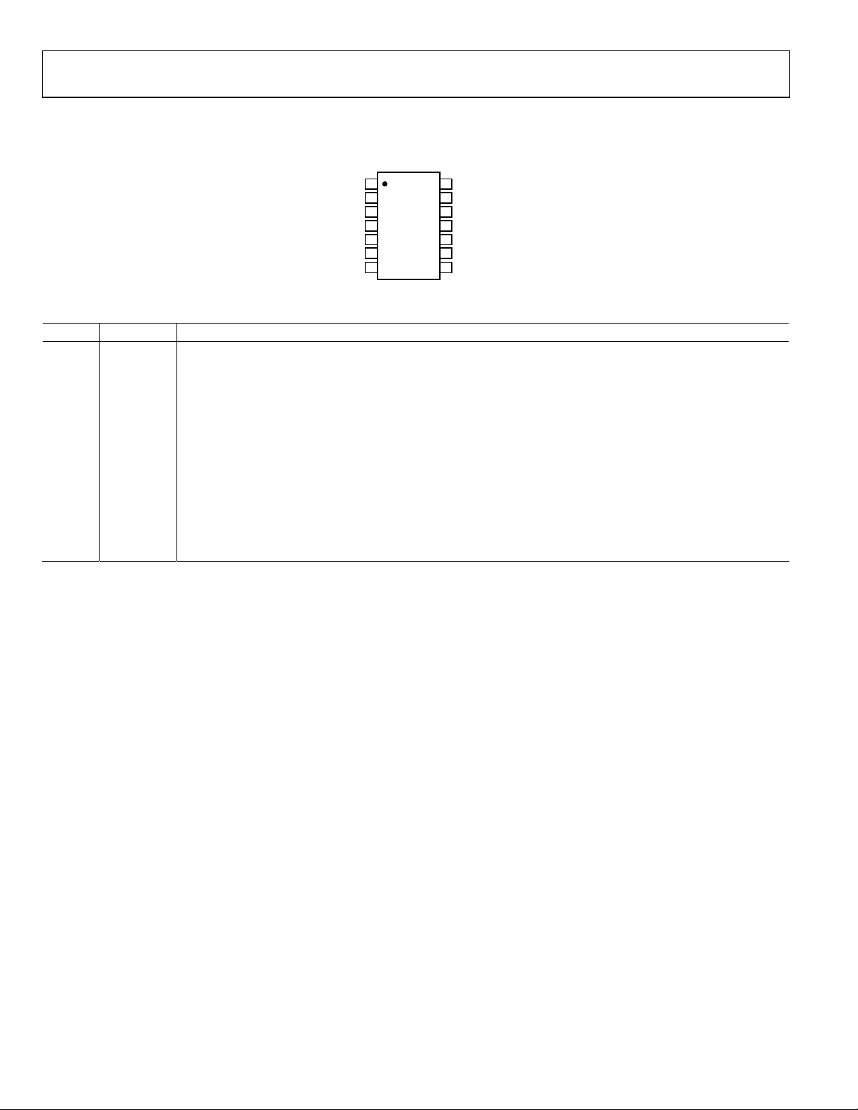
PIN CONFIGURATION AND FUNCTION DESCRIPTIONS
ICOM
ENBL
INPT
MODE
GAIN
DETO
ICOM
1
2
3
AD8367
4
TOP VIEW
(Not to Scale)
5
6
7
14
13
12
11
10
9
8
ICOM
HPFL
VPSI
VPSO
VOUT
DECL
OCOM
02710-002
Figure 2. Pin Configuration
Table 3. Pin Function Descriptions
Pin No. Mnemonic Description
1, 7, 14 ICOM Signal Common. Connect to low impedance ground.
2 ENBL A HI Activates the Device.
3 INPT Signal Input. 200 Ω to ground.
4 MODE Gain Direction Control. HI for positive slope; LO for negative slope.
5 GAIN Gain Control Voltage Input.
6 DETO Detector Output. Provides output current for RSSI function and AGC control.
8 OCOM Power Common. Connect to low impedance ground.
9 DECL Output Centering Loop Decoupling Pin.
10 VOUT Signal Output. To be externally ac-coupled to load.
11 VPSO
Positive Supply Voltage. 2.7 V to 5.5 V. VPSI and VPSO are tied together internally with back-to-back
PN junctions. They should be tied together externally and properly bypassed.
12 VPSI Positive Supply Voltage. 2.7 V to 5.5 V.
13 HPFL High-Pass Filter Connection. A capacitor to ground sets the corner frequency of the output offset control loop.
Rev. A | Page 6 of 24
Page 7
AD8367
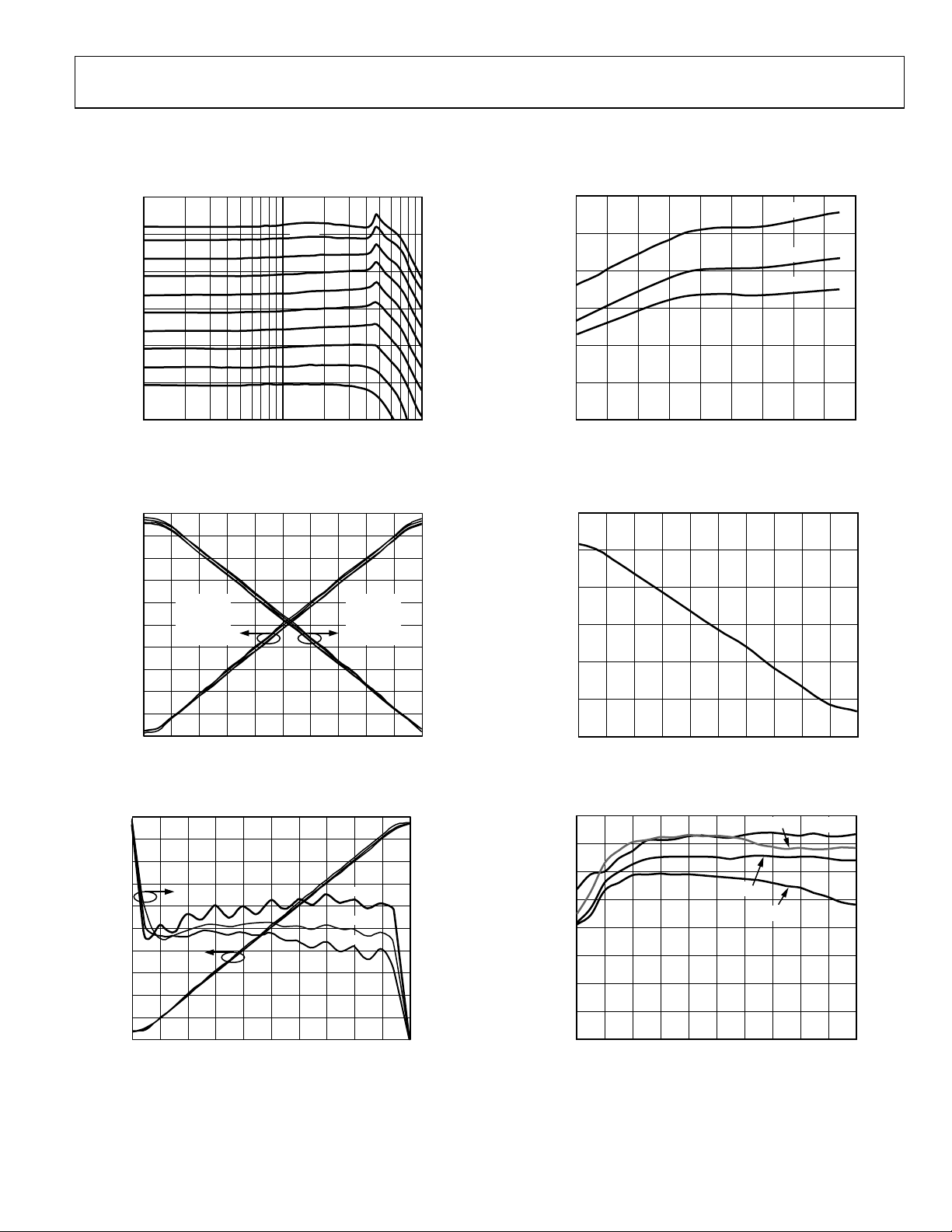
TYPICAL PERFORMANCE CHARACTERISTICS
VS = 5 V, TA = 25°C, system impedance ZO = 200 Ω, V
50
1V
40
30
20
GAIN (dB)
10
0
0.9V
0.8V
0.7V
0.6V
0.5V
0.4V
0.3V
0.2V
0.1V
= 5 V, unless otherwise noted.
MODE
NOISE FIGURE (dB)
10
+85°C
9
+25°C
8
–40°C
7
6
5
–10
10 100 1000
FREQUENCY (MHz)
Figure 3. Gain vs. Frequency for Values of V
45
40
35
30
MODE = 0V
10MHz
70MHz
140MHz
240MHz
–40°C
+25°C
+85°C
GAIN (dB)
25
20
GAIN (dB)
15
10
–5
45
40
35
30
25
20
15
10
5
0
–5
0 1.00.90.80.70.60.50.40.30.20.1
5
0
0 1.00.90.80.70.60.50.40.30.20.1
MODE = 5V
10MHz
70MHz
140MHz
240MHz
Figure 4. Gain vs. V
V
(V)
GAIN
(Mode LO and Mode HI)
GAIN
V
(V)
GAIN
GAIN
02710-003
02710-004
2.0
1.6
1.2
0.8
0.4
0
–0.4
–0.8
–1.2
–1.6
–2.0
Figure 5. Gain Conformance at 70 MHz for T = −40°C, +25°C, and +85°C
LINEARITY ERROR (dB)
02710-005
4
70 25023021019017015013011090
FREQUENCY (MHz)
Figure 6. NF (re 200 Ω) vs. Frequency at Maximum Gain
60
50
40
30
20
NOISE FIGURE (dB)
10
0
OIP3 (dBm)
0 1.00.90.80.70.60.50.40.30.20.1
Figure 7. NF (re 200 Ω) vs. V
40
35
30
25
20
15
10
5
0
0 1.00.90.80.70.60.50.40.30.20.1
V
(V)
GAIN
140MHz
V
(V)
GAIN
Figure 8. OIP3 vs. V
at 70 MHz
GAIN
70MHz
240MHz
GAIN
02710-006
`
02710-007
10MHz
02710-008
Rev. A | Page 7 of 24
Page 8
AD8367
40
33
0
35
30
25
20
OIP3 (dBm re 200Ω)
15
10
10 1000100
Figure 9. OIP3 vs. Frequency for V
4
2
0
–2
–4
FREQUENCY (MHz)
= 500 mV
GAIN
140MHz
10MHz
200MHz
70MHz
28
23
18
OIP3 (dBV rms)
13
8
02710-009
3
11
)
Ω
9
7
5
3
–10
–20
–30
–40
–50
OUTPUT IMD3 (dBc)
–60
–70
–80
10MHz
0 1.00.90.80.70.60.50.40.30.20.1
Figure 12. IMD3 vs. Gain (V
4
2
0
–2
–4
140MHz
V
(V)
GAIN
= 1 V p-p Composite)
OUT
240MHz
70MHz
02710-012
11
)
Ω
9
7
5
3
–6
OUTPUT 1dB COMPRESSION (dBV rms)
–8
0 0.1 0.2 0.3 0.4 0.5 0.6 0.7 0.8 0.9 1.0
Figure 10. Output P1dB vs. V
5
4
3
2
1
0
–1
–2
–3
OUTPUT 1dB COMPRESSION (dBV rms)
–4
–5
10 100 1000
Figure 11. Output P1dB vs. Frequency at V
V
(V)
GAIN
FREQUENCY (MHz)
GAIN
GAIN
= 500 mV
1
OUTPUT 1dB COMPRESSION (dBm re 200
02710-010
–1
–6
OUTPUT 1dB COMPRESSION (dBV rms)
–8
2.5 5.55.04.54.03.53.0
VS (V)
1
OUTPUT 1dB COMPRESSION (dBm re 200
02710-013
–1
Figure 13. Output Compression Point vs. Supply Voltage at 70 MHz,
= 500 mV
V
GAIN
12
)
Ω
11
10
9
8
7
6
5
4
3
OUTPUT 1dB COMPRESSION (dBm re 200
02710-011
2
40
35
)
30
Ω
25
20
15
10
OUTPUT IP3 (dBm re 200
5
0
2.5 5.55.04.54.03.53.0
VS (V)
33
28
23
18
13
8
OUTPUT IP3 (dBV rms)
3
–2
02710-014
–7
Figure 14. Output Third-Order Intercept vs. Supply Voltage at 70 MHz,
= 500 mV
V
GAIN
Rev. A | Page 8 of 24
Page 9

AD8367
250
200
)
Ω
150
100
RESISTANCE (
50
0
0 500400300200100
FREQUENCY (MHz)
Figure 15. Input Resistance and Series Reactance vs. Frequency
= 500 mV
at V
GAIN
90
120
150
210
240
300mV
500mV
700mV
270
Figure 16. Input Reflection Coefficient vs.
Frequency from 10 MHz to 500 MHz for Multiple Values of V
70
60
300
30
330
500mV
700mV
90
300mV
270
60
300
30
330
0180
02710-018
0
–25
–47
–73
–95
–120
)
Ω
SERIES REACTANCE (
02710-015
120
150
210
240
Figure 18. Output Reflection Coefficient vs. Frequency from
10 MHz to 500 MHz for Multiple Values of V
GAIN
0.5
0.4
0.3
0.2
0180
02710-016
V (V)
0.1
0
–0.1
–0.2
–0.3
V
GAIN
V
OUT
TIME (200ns/DIV)
02710-019
Figure 19. AGA Time Domain Response (3 dB Steps)
GAIN
20
25
65
)
60
Ω
55
RESISTANCE (
50
45
40
0 500400300200100
FREQUENCY (MHz)
Figure 17. Output Resistance and Series Reactance vs.
Frequency at V
= 500 mV
GAIN
15
)
Ω
10
5
0
SERIES REACTANCE (
–5
02710-017
–10
Rev. A | Page 9 of 24
20
15
GAIN (dB)
10
5
0
0.1 100k10k1k100101
02710-020
FREQUENCY (kHz)
Page 10

AD8367
+25°C
–40°C
+85°C
16QAM
SINE
IS95FWD
2.0
1.5
1.0
0.5
0
–0.5
–1.0
–1.5
–2.0
–2.5
–3.0
2.0
1.5
1.0
0.5
0
–0.5
–1.0
–1.5
–2.0
–2.5
–3.0
2.5
2.0
1.5
1.0
0.5
0
–0.5
–1.0
–1.5
–2.0
–2.5
LINEARITY ERROR (dB)
02710-021
LINEARITY ERROR (dB)
02710-022
LINEARITY ERROR (dB)
02710-023
0.8
V
= 100pF
AGC
V
OUT
0.7
C
AGC
0.6
V (V)
0.5
0.4
–5
–2
–5
–1
01–52
TIME (Seconds)
Figure 24. AGC Time Domain Response (3 dB Step)
19.0097 19.7297 19.9097 20.0897 20.2697
GAIN SCALING (mV/dB)
Figure 25. Gain Scaling Distribution at 70 MHz
–6.4 –6.2 –6.0 –5.8 –5.6 –5.4 –5.2 –5.0 –4.8
INTERCEPT (dB)
Figure 26. Gain Intercept Distribution at 70 MHz
–5
02710-024
02710-025
02710-026
1.0
0.9
0.8
0.7
0.6
0.5
RSSI (V)
0.4
0.3
0.2
0.1
0
–60 –50 –40 –30 –20 –10 0
70MHz
10MHz
140MHz
240MHz
INPUT LEVEL (dBV rms)
10MHz
70MHz
140MHz
240MHz
Figure 21. AGC RSSI (Voltage on DETO Pin) vs. Input Power at 10 MHz,
70 MHz, 140 MHz, and 240 MHz
1.0
0.9
0.8
0.7
0.6
0.5
RSSI (V)
0.4
0.3
0.2
0.1
0
–60 –50 –40 –30 –20 –10 0
+85°C
–40°C
INPUT LEVEL (dBV rms)
+25°C
Figure 22. AGC RSSI (Voltage on DETO Pin) vs.
Input Power over Temperature at 70 MHz
1.0
0.9
0.8
0.7
0.6
0.5
RSSI (V)
0.4
0.3
0.2
0.1
0
–60 –50 –40 –30 –20 –10 0
INPUT LEVEL (dBV rms)
256QAM
WCDMA
64QAM
Figure 23. AGC RSSI (Voltage on DETO Pin) vs. Input Power
for Various Modulation Schemes
Rev. A | Page 10 of 24
Page 11

AD8367
THEORY OF OPERATION
The AD8367 is a variable gain, single-ended, IF amplifier based
on Analog Devices’ patented X-AMP architecture. It offers
accurate gain control with a 45 dB span and a 3 dB bandwidth
of 500 MHz. It can be configured as a traditional VGA with
50 dB/V gain scaling or as an AGC amplifier by using the built
in rms detector.
Figure 27 is a simplified block diagram of the
amplifier. The main signal path consists of a voltage controlled
0 dB to 45 dB variable attenuator followed by a 42.5 dB fixed
gain amplifier. The AD8367 is designed to operate optimally in
a 200 Ω impedance system.
GAIN
INPT
GAIN INTERPOLATOR
gmgmg
200Ω
m
0dB –5dB –10dB –45dB
ATTENUATOR LADDER
Figure 27. Simplified Architecture
INTEGRATOR
g
m
V
OUT
–42.5dB
OUTPUT
BUFFER
VOUT
02710-027
INPUT ATTENUATOR AND GAIN CONTROL
The variable attenuator consists of a 200 Ω single-ended
resistive ladder that comprises of nine 5 dB sections and an
interpolator that selects the attenuation factor. Each tap point
down the ladder network further attenuates the input signal
by a fixed decibel factor. Gain control is achieved by sensing
different tap points with variable transconductance stages.
Based on the gain control voltage, an interpolator selects which
stage(s) are active. For example, if only the first stage is active,
the 0 dB tap point is sensed; if the last stage is active, the 45 dB
tap point is sensed. Attenuation levels that fall between tap
points are achieved by having neighboring g
simultaneously, creating a weighted average of the discrete
tap point attenuations. In this way, a smooth, monotonic
attenuation function is synthesized, that is, linear-in-dB
with a very precise scaling.
The gain of the AD8367 can be an increasing or decreasing
function of the control voltage, V
, depending on whether
GAIN
the MODE pin is pulled up to the positive supply or down to
ground. When the MODE pin is high, the gain increases with
V
, as shown in Figure 28. The ideal linear-in-dB scaled
GAIN
transfer function is given by
Gain (dB) = 50 × V
where V
is expressed in volts.
GAIN
− 5 (1)
GAIN
Equation 1 contains the gain scaling factor of 50 dB/V (20
mV/dB) and the gain intercept of −5 dB, which represents the
extrapolated gain for V
to +42.5 dB for V
GAIN
= 0 V. The gain ranges from −2.5 dB
GAIN
ranging from 50 mV to 950 mV. The
stages active
m
deviation from Equation 1, that is, the gain conformance error,
is also illustrated in
Figure 28. The ripples in the error are a
result of the interpolation action between
tap points. The AD8367 provides better than ±0.5 dB of
conformance error over >40 dB gain range at 200 MHz
and ±1 dB at 400 MHz.
44
40
36
32
28
24
20
16
GAIN (dB)
12
8
4
0
–4
0 1.00.90.80.70.60.50.40.30.20.1
Figure 28. The gain function can be either an increasing or decreasing
LO MODE
HI MODE
function of V
GAIN
The gain is a decreasing function of V
is low.
Figure 28 also illustrates this mode, which is described by
Gain (dB) = 45 − 50 × V
50dB/V
GAIN
SLOPE
V
(V)
GAIN
, depending on the MODE pin.
when the MODE pin
GAIN
(2)
GAIN
2.0
1.6
1.2
0.8
0.4
0
–0.4
–0.8
–1.2
–1.6
–2.0
–2.4
LINEARITY ERROR (dB)
02710-028
This gain mode is required in AGC applications using the builtin, square-law level detector.
INPUT AND OUTPUT INTERFACES
The AD8367 was designed to operate best in a 200 Ω impedance system. Its gain range, conformance law, noise, and
distortion assume that 200 Ω source and load impedances
are used. Interfacing the AD8367 to other common impedances
(from 50 Ω used at radio frequencies to 1 kΩ presented by data
converters) can be accomplished using resistive or reactive
passive networks, whose design depends on specific system
requirements, such as bandwidth, return loss, noise figure,
and absolute gain range.
The input impedance of the AD8367 is nominally 200 Ω,
determined by the resistive ladder network. This presents a
200 Ω dc resistance to ground, and, in cases where an elevated
signal potential is used, ac coupling is necessary. The input
signal level must not exceed 700 mV p-p to avoid overloading
the input stage. The output impedance is determined by an
internal 50 Ω damping resistor, as shown in
the fact that the output impedance is 50 Ω, the AD8367 should
still be presented with a load of 200 Ω. This implies that the
load is mismatched, but doing so preserves the distortion
performance of the amplifier.
Figure 29. Despite
Rev. A | Page 11 of 24
Page 12

AD8367
V
FROM
INTEGRATOR
B1
V
B2
50Ω
V
OUT
02710-029
Figure 29. A 50 Ω resistor is added to the
output to prevent package resonance.
POWER AND VOLTAGE METRICS
Although power is the traditional metric used in the analysis
of cascaded systems, most active circuit blocks fundamentally
respond to voltage. The relationship between power and voltage
is defined by the impedance level. When input and output
impedance levels are the same, power gain and voltage gain
are identical. However, when impedance levels change between
input and output, they differ. Thus, one must be very careful to
use the appropriate gain for system chain analyses. Quantities
such as OIP3 are quoted in dBV rms as well as dBm referenced
to 200 Ω. The dBV rms unit is defined as decibels relative to
1 V rms. In a 200 Ω environment, the conversion from dBV rms
to dBm requires the addition of 7 dB to the dBV rms value. For
example, a 2 dBV rms level corresponds to 9 dBm.
NOISE AND DISTORTION
Since the AD8367 consists of a passive variable attenuator
followed by a fixed gain amplifier, the noise and distortion
characteristics as a function of the gain voltage are easily
predicted. The input-referred noise increases in proportion to
the attenuation level.
function of V
GAIN
NF of 7.5 dB occurs at maximum gain and increases 1 dB for
every 1 dB reduction in gain. In receiver applications, the
minimum NF should occur at the maximum gain where the
received signal presumably is weak. At higher levels, a lower
gain is needed, and the increased NF becomes less important.
The input-referred distortion varies in a similar manner to the
noise.
Figure 30 illustrates how the third-order intercept point
at the input, IIP3, behaves as a function of V
IIP3 of 20 dBV rms (27 dBm re 200 Ω) occurs at minimum
gain. The IIP3 then decreases 1 dB for every 1 dB increase in
gain. At lower levels, a degraded IIP3 is acceptable. Overall, the
dynamic range, represented by the difference between IIP3 and
NF, remains reasonably constant as a function of gain. The
output distortion and compression are essentially independent
of the gain. At low gains, when the input level is high, input
overload can occur, causing premature distortion.
Figure 30 shows noise figure, NF, as a
for the MODE pin pulled high. The minimum
. The highest
GAIN
60
50
40
30
20
10
00
–10
–20
–30
NF (dB)
02710-030
IIP3 (dBV)
60
50
40
30
20
10
–10
–20
–30
0 1.00.90.80.70.60.50.40.30.20.1
NF
IIP3
V
GAIN
(V)
Figure 30. Noise Figure and Input Third-Order Intercept vs.
SOURCE
= 200 Ω)
Gain (R
OUTPUT CENTERING
To maximize the ac swing at the output of the AD8367, the
output level is centered midway between ground and the supply.
This is achieved when the DECL pin is bypassed to ground via a
shunt capacitor. The loop acts to suppress deviations from the
reference at outputs below its corner frequency while not affecting signals above it, as shown in
corner frequency with no external capacitor is 500 kHz. The
corner frequency can be lowered arbitrarily by adding an
external capacitor, C
(kHz)+=
f
HP
:
HP
10
C
HP
A 100 Ω in series with the C
de-Q the resonant tank that is formed by the bond-wire
inductance and C
. Failure to insert this capacitor can
HP
potentially cause oscillations at higher frequencies at high
gain settings.
FROM
INPUT
Figure 31. The dc output level is centered to midsupply by a control loop
whose corner frequency is determined by C
Figure 31. The maximum
(3)
0.02(nF)
capacitor is recommended to
HP
MAIN
AMPLIFIER
VOUT
g
HPFL
C
HP
R
HP
m
= 1
A
V
DECL
V
MID
02710-031
.
HP
Rev. A | Page 12 of 24
Page 13

AD8367
RMS DETECTION
The AD8367 contains a square-law detector that senses
the output signal and compares it to a calibrated setpoint of
354 mV rms, which corresponds to a 1 V p-p sine wave. This
setpoint is internally set and cannot be modified to change the
AGC setpoint and the resulting VOUT level without using
additional external components. This is described in the
Modifying the AGC Setpoint section.
Any difference between the output and setpoint generates
a current that is integrated by an external capacitor, C
connected from the DETO pin to ground, to provide an AGC
control voltage. There is also an internal 5 pF capacitor on the
DETO pin.
AGC
,
The resulting voltage is used as an AGC bias. For this
application, the MODE pin is pulled low and the DETO pin is
tied to the GAIN pin. The output signal level is then regulated
to 354 mV rms. The AGC bias represents a calibrated rms
measure of the received signal strength (RSSI). Since in AGC
mode the output signal is forced to the 354 mV rms setpoint
(−9.02 dBV rms), Equation 2 can be recast to express the
strength of the received signal, V
bias V
.
DETO
V
(dBV rms) = 54.02 + 50 × V
IN − RMS
, in terms of the AGC
IN-RMS
DETO
where −54.02 dBV rms = −45 dB − 9.02 dBV rms.
For small changes in input signal level, V
characteristic single-pole time constant, τ
proportional to C
τ
(μs) = 10 × C
AGC
AGC
.
(nf)
AGC
responds with a
DETO
, which is
AGC
where the internal 5 pF capacitor is lumped with the external
capacitor to give C
AGC
.
(4)
(5)
Rev. A | Page 13 of 24
Page 14

AD8367
APPLICATIONS
The AD8367 can be configured either as a VGA whose gain
is controlled externally through the GAIN pin or as an AGC
amplifier, using a supply voltage of 2.7 V to 5.5 V. The supply
to the VPSO and VPSI pins should be decoupled using a low
inductance, 0.1 μF surface-mount, ceramic capacitor as close
as possible to the device. Additional supply decoupling can
be provided by a small series resistor. A 10 nF capacitor from
Pin DECL to Pin OCOM is recommended to decouple the
output reference voltage.
INPUT AND OUTPUT MATCHING
The AD8367 is designed to operate in a 200 Ω impedance
system. The output amplifier is a low output impedance voltage
buffer with a 50 Ω damping resistor to desensitize it from load
reactance and parasitics. The quoted performance includes the
voltage division between the 50 Ω resistor and the 200 Ω load.
The AD8367 can be reactively matched to an impedance other
than 200 Ω by using traditional step-up and step down
matching networks or high quality transformers.
the 50 Ω S-parameters for the AD8367 at a V
Tabl e 4 lists
= 750 mV.
GAIN
Minimum-loss, L-pad networks are used on the evaluation
board (see
Figure 45) to allow easy interfacing to standard
50 Ω test equipment. Each pad introduces an 11.5 dB power
loss (5.5 dB voltage loss).
1
0.3333
–0.3333
R
SOURCE
0.3333 1 3
SERIES L
SHUNT C
3
Z
IN
–3
Figure 32 illustrates an example where the AD8367 is matched
to 50 Ω at 140 MHz. As shown in the Smith Chart, the input
matching network shifts the input impedance from Z
to 50 Ω
IN
with an insertion loss of <2 dB over a 5 MHz bandwidth. For
the output network, the 50 Ω load is made to present 200 Ω to
the AD8367 output.
Tabl e 5 provides the component values
required for 50 Ω matching at several frequencies of interest.
When added loss and noise can be tolerated, a resistive pad can
be used to provide broadband, near-matched impedances at the
device terminals and the terminations.
R
SOURCE
fC = 140MHz, ZIN = 197 – j34.2, R
XS
IN
100nH
XP
IN
8.2pF
50Ω
V
S
Z
IN
Figure 32. Reactive Matching Example for f = 140 MHz
Z
IN
–1
AD8367
SOURCE
Z
OUT
= 50Ω
Z
C
0.1μF
LOAD
AC
XP
OUT
120nH
XS
13pF
OUT
R
LOAD
50Ω
02710-032
Table 4. S-Parameters for 200 Ω System for VS = 5 V and V
= 0.75 V
GAIN
Frequency (MHz) S11 S21 S12 S22
10
70
140
190
240
0.04 ∠ −43.8° 41.1 ∠ 178.8° 0.0003 ∠ 76.1° 0.56 ∠ −179.3°
0.09 ∠ −81.5° 43.6 ∠ 163.4° 0.0002 ∠ 63.7° 0.55 ∠ +176.1°
0.17 ∠ −103.4° 48.0 ∠ 141.4° 0.0009 ∠ 130.8° 0.56 ∠ +170.2°
0.21 ∠ −111.7° 47.5 ∠ 124.0° 0.0017 ∠ 96.8° 0.54 ∠ +166.5°
0.26 ∠ −103.8° 48.3 ∠ 107.6° 0.0018 ∠ 113.5° 0.48 ∠ +164.6°
Table 5. Reactive Matching Components for a 50 Ω System where R
Frequency (MHz) XS
IN
XPIN (pF) XS
SOURCE
= 50 Ω, R
= 50 Ω
LOAD
(pF) XP
OUT
OUT
10 1.5 μH 120 180 1.8 μH
70 220 nH 15 27 270 nH
140 100 nH 8.2 13 120 nH
190 82 nH 2.7 10 100 nH
240 68 nH 1.5 7 82 nH
Rev. A | Page 14 of 24
Page 15

AD8367
VGA OPERATION
The AD8367 is a general-purpose VGA suitable for use in a
wide variety of applications where voltage control of gain is
needed. While having a 500 MHz bandwidth, its use is not
limited to high frequency signal processing. Its accurate,
temperature- and supply-stable linear-in-dB scaling is
valuable wherever it is important to have a more dependable
response to the control voltage than is usually offered by VGAs
of this sort. For example, there is no preclusion to its use in
speech-bandwidth systems.
Figure 33 shows the basic connections. The CHP capacitor at
Pin HPFL can be used to alter the high-pass corner frequency of
the signal path and is associated with the offset control loop that
eliminates the inherent variation in the internal dc balance of the
signal path as the gain is varied (offset ripple). This frequency
should be chosen to be about a decade below the lowest frequency
component of the signal. If made much lower than necessary, the
offset loop is not able to track the variations that occur when there
are rapid changes in V
. The control of offset is important even
GAIN
when the output is ac-coupled because of the potential reduction of
the upper and lower voltage range at this pin.
However, in many applications these components are
unnecessary because an internal network provides a default
high-pass corner of about 500 kHz. For C
= 1 nF, the
HP
modified corner is at ~10 kHz; it scales downward with
increasing capacitance.
Figure 20 shows representative
response curves for the indicated component values.
V
C3
0.1μF
P
02710-033
V
V
GAIN
C1
AD8367
ICOM1ICOM
ENBL2HPFL
3
IN
INPT
MODE4VPSO
GAIN5VOUT
DETO6DECL
ICOM7OCOM
VPSI
1μF
C
HP
10nF
C5
10nF
R
100Ω
14
13
12
11
10
9
8
HP
C4
0.1μF
R6
4.7ΩR54.7Ω
C2
0.1μF
VOUT
Figure 33. Basic Connections for Voltage Controlled Gain Mode
MODULATED GAIN MODE
The AD8367 can be used as a means of modulating the signal
level. Keep in mind, however, that the gain is a nonlinear
(exponential) function of V
normal amplitude-modulation functions. The small signal
bandwidth of the gain interface is ~5 MHz, and the slew rate
is of the order of ±500 dB/μs. During gain slewing from close
to minimum to maximum gain (or vice versa), the internal
interpolation processes in an X-AMP-based VGA rapidly
scan the full range of gain values. The gain and offset ripple
associated with this process can cause transient disturbances
in the output. Therefore, it is inadvisable to use high amplitude
pulse drives with rise and fall times below 200 ns.
; thus, it is not suitable for
GAIN
AGC OPERATION
The AD8367 can be used as an AGC amplifier, as shown in
Figure 34. For this application, the accurate internal, square-law
detector is employed. The output of this detector is a current
that varies in polarity, depending on whether the rms value of
the output is greater or less than its internally-determined
setpoint of 354 mV rms. This is 1 V p-p for sine-wave signals,
but the peak amplitude for other signals, such as Gaussian
noise, or those carrying complex modulation, is invariably
somewhat greater. However, for all waveforms having a crest
factor of <5, and when using a supply voltage of 4.5 V to 5.5 V,
the rms value is correctly measured and delivered at V
When using lower supplies, the rms value of V
OUT
(the setpoint is determined by a band gap reference), but the
peak crest factor capacity is reduced.
The gain pin is connected to the base of a transistor internally
and thus requires only 1 μA of current drive. The output of the
detector is delivered to Pin DETO. The detector can source up
to 60 μA and can sink up to 11 μA. For a sine-wave output
signal, and under conditions where the AGC loop is settled, the
detector output also takes the form of a sine-wave, but at twice
the frequency and having a mean value of 0. If the input to the
amplifier increases, the mean of this current also increases and
charges the external loop filter capacitor, C
positive voltages. Conversely, a reduction in V
, toward more
AGC
below the
OUT
setpoint of 354 mV rms causes this voltage to fall toward
ground. The capacitor voltage is the AGC bias; this can be
used as a received signal strength indicator (RSSI) output
and is scaled exactly as V
AD8367
ICOM1ICOM
ENBL2HPFL
INPT
3
MODE4VPSO
GAIN5VOUT
AGC
DETO6DECL
ICOM7OCOM
Figure 34. Basic Connections for AGC Operation
V
V
AGC
C
0.1μF
IN
, that is, 20 mV/dB.
GAIN
C1
1μF
C
HP
14
10nF
C5
10nF
100Ω
VPSI
13
12
11
10
9
8
R
HP
C4
0.1μF
R6
4.7ΩR54.7Ω
C2
0.1μF
A valuable feature of using a square law detector is that the
RSSI voltage is a true reflection of signal power and can be
converted to an absolute power measurement for any given
source impedance. The AD8367 can thus be employed as a
true-power meter, or decibel-reading ac voltmeter, as distinct
from its basic amplifier function.
The AGC mode of operation requires that the correct gain
direction is chosen. Specifically, the gain must fall as V
increases to restore the needed balance against the setpoint.
Therefore, the MODE pin must be pulled low. This accurate
leveling function is shown in
Figure 35, where the rms output is
.
OUT
is unaffected
V
P
C3
0.1μF
VOUT
02710-034
AGC
Rev. A | Page 15 of 24
Page 16

AD8367
held to within 0.1 dB of the setpoint for >35 dB range of
input levels.
The dynamics of this loop are controlled by C
conjunction with an on-chip equivalent resistance, R
10 kΩ which form an effective time-constant T
acting in
AGC
= R
AGC
, of
AGC
AGC CAGC
.
The loop thus operates as a single-pole system with a loop
bandwidth of 1/(2π T
). Because the gain control function is
AGC
linear in decibels, this bandwidth is independent of the absolute
signal level.
change in input signal level with C
It is important to understand that R
shunt with C
Figure 36 illustrates the loop dynamics for a 30 dB
= 100 pF.
AGC
–1.2
–1.3
–1.4
)
–1.5
Ω
–1.6
–1.7
–1.8
POUT (dBm re 200
–1.9
–2.0
–2.1
–2.2
–50 –40 –30 –20 –10 0 10
Figure 35. Leveling Accuracy of the AGC Function
1.0
0.8
0.6
0.4
(arb)
OUT
0.2
(V); V
0
ACG
V
–0.2
–0.4
–0.6
0 5 10 15 20 25 30 35 40
Figure 36. AGC Response to a 32 dB Step in Input Level (f = 50 MHz)
. Rather, the error-correction process is that of a
AGC
PIN (dBm re 200Ω)
V
AGC
V
OUT
TIME (μs)
does not act as if in
AGC
02710-035
02710-036
true integrator, to guarantee an output that is exactly equal in
rms amplitude to the specified setpoint. For large changes in
input level, the integrating action of this loop is most apparent.
The slew rate of V
is determined by the peak output current
AGC
from the detector and the capacitor. Thus, for a representative
value of C
= 3 nF, this rate is about 20 V rms or 10 dB/μs,
AGC
while the small-signal bandwidth is 1 kHz.
Most AGC loops incorporating a true error-integrating
technique have a common weakness. When driven from an
increasingly larger signal, the AGC bias increases to reduce the
gain. However, eventually the gain falls to its minimum value,
for which further increase in this bias has no effect on the gain.
That is, the voltage on the loop capacitor is forced progressively
higher because the detector output is a current, and the AGC
bias is its integral. Consequently, there is always a precipitous
increase in this bias voltage when the input to the AD8367
exceeds that value that overdrives the detector, and because the
minimum gain is −2.5 dB, that happens for all inputs 2.5 dB
greater than the setpoint of ~350 mV rms. If possible, the user
should ensure that this limitation is preserved, preferably with a
guard-band of 5 dB to 10 dB below overload
In some cases, if driven into AGC overload, the AD8367
requires unusually long times to recover; that is, the voltage
at DETO remains at an abnormally high value and the gain is at
its lowest value. To avoid this situation, it is recommended that
a clamp be placed on the DETO pin, as shown in
AD8367
1 14
+V
S
C
AGC
0.1μF
V
RB
0.5V
RA
Q1
2N2907
Figure 37. External Clamp to Prevent AGC Overload.
The resistive divider network, RA and RB, should be designed
such that the base of Q1 is driven to 0.5 V.
2 13
3 12
4 11
AGC
5 10
6 9
7 8
MODE
GAIN
DETO
ICOM
Figure 37.
02710-037
MODIFYING THE AGC SETPOINT
If an AGC setpoint other than the internal one is desired, an
external detector must be used.
that uses an external true-rms detector and error integrator to
operate the AD8367 as a closed-loop AGC system with a usersettable operating level.
The AD8361 (U2) produces a dc output level that is
proportional to the rms value of its input, taken as a sample
of the AD8367 (U1) output. This dc voltage is compared to
an externally-supplied setpoint voltage, and the difference is
integrated by the AD820 (U3) to form the gain control voltage
that is applied to the GAIN input of the AD8367 through the
divider composed of R4 and R5. This divider is included in
order to minimize overload recovery time of the loop by having
the integrator saturate at a point that only slightly overdrives the
gain control input of the AD8367. The scale factor at V
influenced by the values of R4 and R5; for the values shown, the
factor is 86 mV/dB.
Figure 38 shows a method
AGC
is
Rev. A | Page 16 of 24
Page 17

AD8367
Ω
(
)
AD8367
ICOM
INPUT
J1
R6
57.6Ω
V
g
10kΩ
10nF
R5
1
ENBL2HPFL
INPT
3
MODE4VPSO
GAIN
5
DETO
6
ICOM
7
U1
ICOM
VPSI
VOUT
DECL
OCOM
R4
33kΩ
Figure 38. Example of Using an External Detector to Form an AGC Loop
Note that in this circuit the AD8367’s MODE pin must be
pulled high to obtain correct feedback polarity because the
integrator inverts the polarity of the feedback signal.
The relationship between the setpoint voltage and the rms
output voltage of the AD8367 is
2.2
10nF
C
HP
10nF
C5
10nF
R
HP
100Ω
6
0.1μF
0.1μF
C1
3.3nF
4
U3
AD820
7
5V
2
3
10nF
R1
200kΩ
R3
82kΩ
V
14
13
12
11
10
9
8
V
AGC
The component values shown in
SET
5V
V
INTO A
OUT
200Ω LOAD
U2
AD8361
VPOS1SREF
IREF2VRMS
RFIN3FLTR
4
PWDN
20pF
150kΩ
C2
0.27μF
8
7
6
5
COMM
R2
Vrms
12kΩ
2710-038
Figure 38 were chosen for a
64-QAM signal at 500 kS/s at a carrier frequency of 150 MHz.
The response time of the loop as shown is roughly 5 ms for
an abrupt input level change of 40 dB.
Figure 41 shows the
dynamic performance of the loop with a step-modulated
CW signal applied to the input for a V
of about 1 V.
SET
R1
+
225
VV
−
×=
SETRMSOUT
(6)
7.5225
×
where 225 is the input resistance of the AD8361 and 7.5 is its
conversion gain. For R1 = 200 Ω, this reduces to V
OUT –RMS
= V
SET
× 0.25.
Capacitor C2 sets the averaging time for the rms detector. This
should be made long enough to provide sufficient smoothing of
the detector’s output in the presence of the modulation on the
RF signal. A level fluctuation of less than 1 dB (<5% to 10%) p-p
at the AD8361’s output is a reasonable value. A considerably
longer time constant needlessly lowers the AGC bandwidth,
while a short time constant can degrade the accuracy of the
true-rms measurement process. Components C1, R2, and R3
set the control loop’s bandwidth and stability. The maximum
stable loop bandwidth is limited by the rms detector’s averaging
time constant as previously discussed.
For an input signal consisting of a 4.096 MS/s QPSK modulated
carrier, the relationship between V
this setup is shown in
Figure 39. The exponential shape reflects
and the output power for
SET
the linear-in-magnitude response of the AD8361. The adjacent
channel power ratio (ACPR) as a function of output power is
illustrated in
Figure 40. The minima occur where the distortion
and integrated noise powers cross over.
For a linear-in-dB response, detectors such as the AD8318 or
the AD8362 can be used in place of the AD8361.
4.0
3.5
3.0
2.5
(V)
2.0
SET
V
1.5
1.0
0.5
0
–20 1050–5–10–15
POUT (dBm INTO 200Ω)
Figure 39. AGC Setpoint Voltage vs. Output Power
(QPSK: 4.096 MS/s; α = 0.22; 1 User)
10MHz
380MHz
02710-039
Rev. A | Page 17 of 24
Page 18

AD8367
–20
–25
–30
–35
–40
ACPR (dBc)
–45
–50
–55
–60
–20 –15 –10 –5 0 5 10
380MHz
POUT (dBm INTO 200Ω)
140MHz
10MHz
70MHz
02710-041
Figure 40. ACPR vs. Output Power for QPSK Waveform
(QPSK: 4.096 MS/s; α = 0.22; 1 User)
Table 6. Suggested Component Values for External AGC Detector Circuit
Modulation Type Rate Sys/s C1 (μF) C2 (μF) R2 (kΩ) R3 (kΩ)
QPSK 1.23 M 0.0022 0.033 150 62
QPSK 4 M 0.0022 0.015 150 39
π/4 DQPSK 24.3 K 0.033 0.68 150 51
64 QAM 100 K 0.015 1.5 150 51
64 QAM 500 K 0.0068 0.33 150 62
64 QAM 4 M 0.0022 0.068 150 100
1.0
V
0.5
0
(arb)
OUT
–0.5
Vg (V); V
–1.0
–1.5
–2.0
0 0.005 0.010 0.015 0.020 0.025 0.030 0.035
V
OUT
TIME (Seconds)
g
02710-040
0.040
Figure 41. AGC Dynamic Response: 8367 AGC with an External Detector
Rev. A | Page 18 of 24
Page 19

AD8367
EVALUATION BOARD
Figure 42 shows the schematic of the AD8367 evaluation board. The board is powered by a single supply of 2.7 V to 5.5 V.
R7
INPUT
SW2
10kΩ
C1
1μF
C
HP
10nF
C5
10nF
R
HP
100Ω
R4
174Ω
14
13
12
11
10
9
8
C
AGC
0.1μF
LK1
TP3
MODE
R1
R2
174Ω
TP4
GAIN
J1
57.6Ω
SW1
AD8367
ICOM
1
ENBL
2
3
INPT
MODE4VPSO
5
GAIN
DETO
6
7
ICOM
ICOM
HPFL
VPSI
VOUT
DECL
OCOM
R6
4.7ΩR54.7Ω
C2
0.1μF
C4
0.1μF
Figure 42. Evaluation Board Schematic
R1
57.6Ω
C3
0.1μF
TP1
J2
V
P
OUTPUT
02710-042
02710-043
02710-044
Figure 43. Layout of Component Side Figure 44. Silkscreen of Component Side
Rev. A | Page 19 of 24
Page 20

AD8367
Tabl e 7 details the various configuration options of the evaluation board.
Table 7. Evaluation Board Configuration Options
Component Function Default Condition
TP1, TP2 Supply and Ground Vector Pins. Not Applicable
TP3, TP4 Mode and Gain Vector Pins. Not Applicable
SW1
VGA/AGC Select: Used to select VGA (Position A) or AGC (Position B) mode of
operation. SW2 must be set for Position A for AGC mode of operation.
SW2
LK1
MODE Select. Used to select positive or negative VGA slope. Set to Position B for an
increasing gain with V
, Position A for decreasing gain law.
GAIN
Device Enable. When LK1 is installed, the ENBL pin is connected to the positive supply
and the AD8367 is in operating mode.
R1, R2
Input Interface. R1 and R2 are used to provide an L-pad impedance-transforming
network. The broadband matching network transforms a 50 Ω source to match a
200 Ω load with 11.5 dB of insertion loss.
R3, R4, C4
Output Interface. R3 and R4 are used to transform a 50 Ω load termination to look like
a 200 Ω load with 11.5 dB of insertion loss. The ac coupling capacitor, C4, can be
increased to obtain a lower high-pass corner frequency.
C1, C2, C3, R5, R6
Power Supply Decoupling. The nominal supply decoupling consists of a 1 μF capacitor
to ground, a 4.7 Ω series resistor, and a 0.1 μF capacitor to ground. The same
decoupling network should be used on both the VPSI and VPSO supply lines.
C5 Internal Supply Decoupling. Capacitor C5 provides midsupply decoupling. C5 = 10 nF (Size 0603)
C
HP
C
AGC
Filter Capacitor. HPFL capacitor, sets the high-pass corner frequency.
AGC Filter Capacitor. Capacitor, CAGC, sets closed-loop AGC response time. C
R7 Mode Pull-Up Resistor. R7 = 10 kΩ (Size 0805)
R
HP
High-Pass Filter Resistor. RHP = 100 Ω (Size)
SW1 = A
SW2 = B
LK1 = Installed
R1 = 57.6 Ω (Size 0603)
R2 = 174 Ω (Size 0603)
R3 = 57.6 Ω (Size 0603)
R4 = 174 Ω (Size 0603)
C4 = 0.1 μF (Size 0603)
C1 = 1 μF (Size 0603)
R5 = R6 = 4.7 Ω (Size 0805)
C2 = C3 = 0.1 μF (Size 0603)
= 0.01 μF (Size 0805)
C
HP
R
= 0 Ω (Size 0603)
HP
= 0.1 μF (Size 0805)
AGC
CHARACTERIZATION SETUP AND METHODS
Minimum-loss, L-pad matching networks were used to
interface standard 50 Ω. A test equipment to the 200 Ω input
impedance during the characterization process. Using a 57.6 Ω
shunt resistor followed by a 174 Ω series resistor provides a
broadband match between the 50 Ω test equipment and the
200 Ω device impedance, as illustrated in
insertion loss of this network is 11.5 dB.
Figure 45. The
AD8367
174Ω
57.6Ω
Figure 45. Characterization Test Setup
174Ω
57.6Ω
02710-045
Rev. A | Page 20 of 24
Page 21

AD8367
OUTLINE DIMENSIONS
5.10
5.00
4.90
1.05
1.00
0.80
4.50
4.40
4.30
PIN 1
14
0.65
BSC
0.15
0.30
0.05
0.19
COMPLIANT TO JEDEC STANDARDS MO-153AB-1
8
6.40
BSC
71
1.20
MAX
SEATING
PLANE
0.20
0.09
COPLANARITY
0.10
8°
0°
0.75
0.60
0.45
Figure 46. 14-Lead Thin Shrink Small Outline Package [TSSOP]
(RU-14)
Dimension shown millimeters
ORDERING GUIDE
Model Temperature Range Package Description Package Option
AD8367ARU −40°C to +85°C 14-Lead TSSOP, Tube RU-14
AD8367ARU-REEL-7 −40°C to +85°C 14-Lead TSSOP, 7" Tape and Reel RU-14
AD8367ARUZ
AD8367ARUZ-RL7
AD8367-EVAL Evaluation Board
1
Z = Pb-free part.
1
1
−40°C to +85°C 14-Lead TSSOP, Tube RU-14
−40°C to +85°C 14-Lead TSSOP, 7" Tape and Reel RU-14
Rev. A | Page 21 of 24
Page 22

AD8367
NOTES
Rev. A | Page 22 of 24
Page 23

AD8367
NOTES
Rev. A | Page 23 of 24
Page 24

AD8367
NOTES
© 2005 Analog Devices, Inc. All rights reserved. Trademarks and
registered trademarks are the property of their respective owners.
C02710–0–7/05(A)
Rev. A | Page 24 of 24
 Loading...