

DC to 600 MHz,
K
FEATURES
Matched pair of differential, digitally controlled VGAs
Gain range: 4.5 dB to 20.25 dB
0.25 dB gain step size
Operating frequency
DC to 150 MHz (2 V p-p)
3 dB bandwidth: 600 MHz
Noise figure (NF)
11.4 dB at 10 MHz at maximum gain
18 dB at 10 MHz at minimum gain
OIP3: 45 dBm at 10 MHz
HD2/HD3
Better than −90 dBc for 2 V p-p output at 10 MHz at
maximum gain
Differential input and output
Adjustable output common-mode
Optional dc output offset correction
Serial/parallel mode gain control
Power-down feature
Single 5 V supply operation
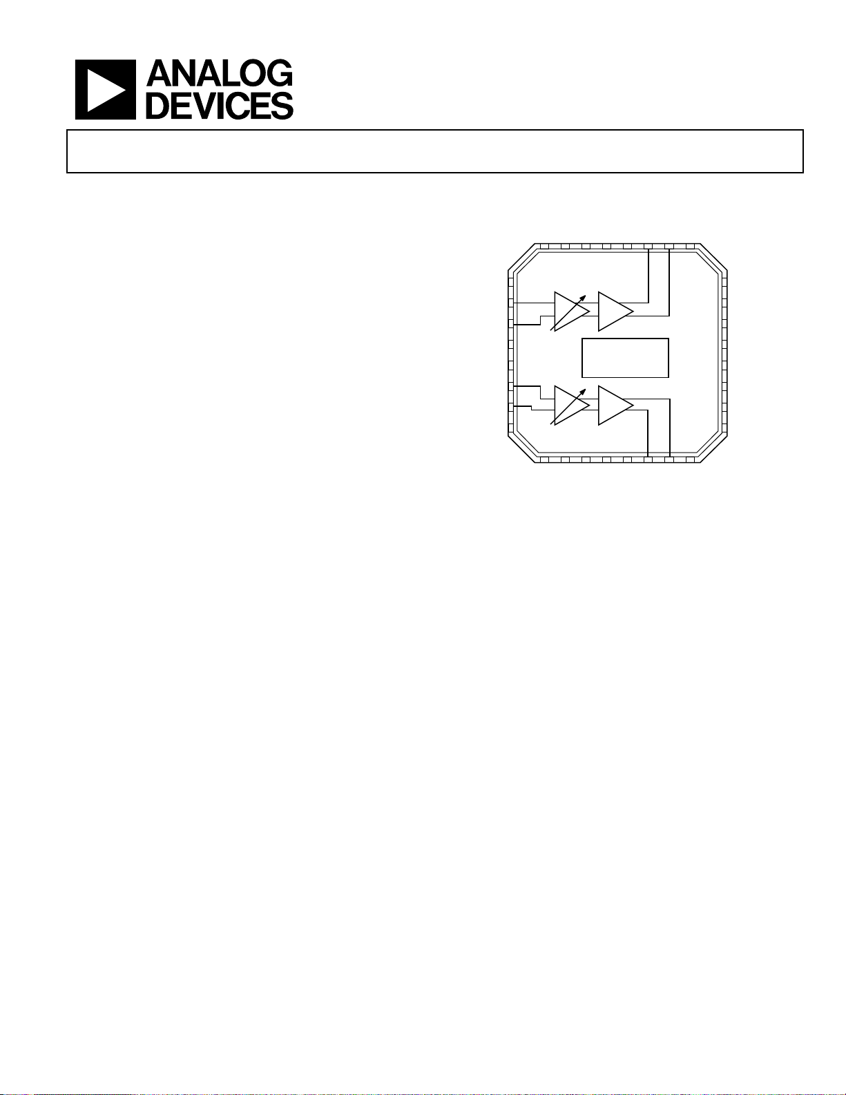
Dual-Digital Variable Gain Amplifiers
AD8366
FUNCTIONAL BLOCK DIAGRAM
VCMA
VPSOA
OPPA
OPMA
OPPB
SENB
BIT0/CS
BIT1/SDAT
BIT2/SCL
BIT3
OCOM
BIT4
BIT 5
DENA
DENB
OPMB
07584-001
DECA
OFSA
CCMA
VPSIA
IPPA
IPMA
ENBL
ICOM
IPMB
IPPB
VPSIB
DECB
DIGITAL GAIN
CONTROL L OGIC
OFSB
CCMB
VCMB
VPSOB
Figure 1.
APPLICATIONS
Baseband I/Q receivers
Diversity receivers
Wideband ADC drivers
GENERAL DESCRIPTION
The AD8366 is a matched pair of fully differential, low noise and
low distortion, digitally programmable variable gain amplifiers
(VGAs). The gain of each amplifier can be programmed separately
or simultaneously over a range of 4.5 dB to 20.25 dB in steps of
0.25 dB. The amplifier offers flat frequency performance from dc
to 70 MHz, independent of gain code.
The AD8366 offers excellent spurious-free dynamic range, suitable
for driving high resolution analog-to-digital converters (ADCs).
The NF at maximum gain is 11.4 dB at 10 MHz and increases
~2 dB for every 4 dB decrease in gain. Over the entire gain range,
the HD3/HD2 are better than −90 dBc for 2 V p-p at the output at
10 MHz into 200 Ω. The two-tone intermodulation distortion of
−90 dBc into 200 Ω translates to an OIP3 of 45 dBm (38 dBVrms).
The differential input impedance of 200 provides a well-defined
termination. The differential output has a low impedance of ~25 .
The output common-mode voltage defaults to V
/2 but can
POS
be programmed via the VCMA and VCMB pins over a range
of voltages. The input common-mode voltage also defaults
to V
/2 but can be driven down to 1.5 V. A built-in, dc offset
POS
compensation loop can be used to eliminate dc offsets from prior
stages in the signal chain. This loop can also be disabled if dccoupled operation is desired.
The digital interface allows for parallel or serial mode gain
programming. The AD8366 operates from a 4.75 V to 5.25 V
supply and consumes typically 180 mA. When disabled, the
part consumes roughly 3 mA. The AD8366 is fabricated using
Analog Devices, Inc., advanced silicon-germanium bipolar
process, and it is available in a 32-lead exposed paddle LFCSP
package. Performance is specified over the −40°C to +85°C
temperature range.
Rev. A
Information furnished by Analog Devices is believed to be accurate and reliable. However, no
responsibility is assumed by Anal og Devices for its use, nor for any infringements of patents or ot her
rights of third parties that may result from its use. Specifications subject to change without notice. No
license is granted by implication or otherwise under any patent or patent rights of Analog Devices.
Trademarks and registered trademarks are the property of their respective owners.
One Technology Way, P.O. Box 9106, Norwood, MA 02062-9106, U.S.A.
Tel: 781.329.4700 www.analog.com
Fax: 781.461.3113 ©2010-2011 Analog Devices, Inc. All rights reserved.

AD8366
TABLE OF CONTENTS
Features.............................................................................................. 1
Applications....................................................................................... 1
Functional Block Diagram ..............................................................1
General Description......................................................................... 1
Revision History ...............................................................................2
Specifications..................................................................................... 3
Parallel and Serial Interface timing............................................ 5
Absolute Maximum Ratings............................................................ 6
ESD Caution.................................................................................. 6
Pin Configuration and Function Descriptions............................. 7
Typical Performance Characteristics............................................. 8
Circuit Description......................................................................... 15
Inputs ...........................................................................................15
Outputs........................................................................................ 15
Output Differential Offset Correction .................................... 15
Output Common-Mode Control ............................................. 15
Gain Control Interface............................................................... 16
Applications Information.............................................................. 17
Basic Connections...................................................................... 17
Direct Conversion Receiver Design......................................... 18
Quadrature Errors and Image Rejection................................. 18
Low Frequency IMD3 Performance ........................................ 19
Baseband Interface..................................................................... 21
Characterization Setups................................................................. 22
Evaluation Board............................................................................ 25
Outline Dimensions....................................................................... 28
Ordering Guide .......................................................................... 28
REVISION HISTORY
3/11—Rev. 0 to Rev. A
Changes to Table 2, Internal Power Dissipation Value................ 6
10/10—Revision 0: Initial Version
Rev. A | Page 2 of 28

AD8366
SPECIFICATIONS
VS = 5 V, TA = 25°C, ZS = 200 Ω, ZL = 200 Ω, f = 10 MHz, unless otherwise noted.
Table 1.
Parameter Test Conditions/Comments Min Typ Max Unit
DYNAMIC PERFORMANCE
Bandwidth 3 dB; all gain codes 600 MHz
1 dB; all gain codes 200 MHz
Slew Rate Maximum gain 1100 V/μs
Minimum gain 1500 V/μs
INPUT STAGE IPPA, IPMA, IPPB, IPMB
Linear Input Swing At minimum gain AV = 4.5 dB, 1 dB gain compression 3.6 V p-p
Differential Input Impedance 217 Ω
Minimum Input Common-Mode Voltage 1.5 V
Maximum Input Common-Mode Voltage V
Input pins left floating V
GAIN
Minimum Voltage Gain 4.5 dB
Maximum Voltage Gain 20.25 dB
Gain Step Size All gain codes 0.25 dB
Gain Step Accuracy All gain codes ±0.25 dB
Gain Flatness Maximum gain, DC to 70 MHz 0.1 dB
Gain Mismatch Channel A/Channel B at minimum/maximum gain code 0.1 dB
Group Delay Flatness All gain codes, 20% fractional bandwidth, fC < 100 MHz <0.5 ns
Mismatch Channel A and Channel B at same gain code 2 ps
Gain Step Response Maximum gain to minimum gain 30 ns
Minimum gain to maximum gain 60 ns
Common-Mode Rejection Ratio −66.2 dB
OUTPUT STAGE OPPA, OPMA, OPPB, OPMB, VCMA, VCMB
Linear Output Swing 1 dB gain compression 6 V p-p
Differential Output Impedance 28 Ω
Output DC Offset Inputs shorted, offset loop disabled at
minimum/maximum gain
Inputs shorted, offset loop enabled (across all gain codes) 10 mV
Minimum Output Common-Mode Voltage HD3, HD2 > −90 dBc, 2 V p-p output 1.6 V
Maximum Output Common-Mode Voltage HD3, HD2 > −90 dBc, 2 V p-p output 3 V
VCMA and VCMB left floating V
Common-Mode Setpoint Input Impedance 4 kΩ
NOISE/DISTORTION
3 MHz
Noise Figure Maximum gain 11.3 dB
Minimum gain 18.2 dB
Second Harmonic 2 V p-p output, maximum gain −82 dBc
2 V p-p output, minimum gain −82 dBc
Third Harmonic 2 V p-p output, maximum gain −87 dBc
2 V p-p output, minimum gain −90 dBc
OIP31 2 V p-p composite, maximum gain 34 dBVrms
2 V p-p composite, minimum gain 35 dBVrms
OIP21 2 V p-p composite, maximum gain 76 dBVrms
2 V p-p composite, minimum gain 76 dBVrms
Output 1 dB Compression Point1 Maximum gain 6.7 dBVrms
Minimum gain 6.9 dBVrms
−10/−30 mV
/2 + 0.075 V
POS
/2 V
POS
/2 V
POS
Rev. A | Page 3 of 28

AD8366
Parameter Test Conditions/Comments Min Typ Max Unit
10 MHz
Noise Figure Maximum gain 11.4 dB
Minimum gain 18 dB
Second Harmonic 2 V p-p output, maximum gain −97 dBc
2 V p-p output, minimum gain −96 dBc
Third Harmonic 2 V p-p output, maximum gain −97 dBc
2 V p-p output, minimum gain −90 dBc
OIP31 2 V p-p composite, maximum gain 38 dBVrms
2 V p-p composite, minimum gain 36 dBVrms
OIP21 2 V p-p composite, maximum gain 72 dBVrms
2 V p-p composite, minimum gain 76 dBVrms
Output 1 dB Compression Point1 Maximum gain 7 dBVrms
Minimum gain 6.7 dBVrms
50 MHz
Noise Figure Maximum gain 11.8 dB
Minimum gain 18.2 dB
Second Harmonic 2 V p-p output, maximum gain −82 dBc
2 V p-p output, minimum gain −84 dBc
Third Harmonic 2 V p-p output, maximum gain −80 dBc
2 V p-p output, minimum gain −71 dBc
OIP31 2 V p-p composite, maximum gain 32 dBVrms
2 V p-p composite, minimum gain 26 dBVrms
OIP21 2 V p-p composite, maximum gain 71 dBVrms
2 V p-p composite, minimum gain 78 dBVrms
Output 1 dB Compression Point1 Maximum gain 6.7 dBVrms
Minimum gain 6.7 dBVrms
DIGITAL LOGIC SENB, DENA, DENB, BIT0, BIT1, BIT2, BIT3, BIT4, BIT5
Input High Voltage, V
Input Low Voltage, V
Input Capacitance, CIN 1 pF
Input Resistance, RIN 50 kΩ
SPI INTERFACE TIMING SENB = high
f
Serial clock frequency (maximum) 44.4 MHz
SCLK
t1 CS rising edge to first SCLK rising edge (minimum) 7.5 ns
t2 SCLK high pulse width (minimum) 7.5 ns
t3 SCLK low pulse width (minimum) 15 ns
t4 SCLK falling edge to CS low (minimum) 7.5 ns
t5 SDAT setup time (minimum) 7.5 ns
t6 SDAT hold time (minimum) 15 ns
PARALLEL PORT TIMING SENB = low
t7 DENA/DENB high pulse width (minimum) 7.5 ns
t8 DENA/DENB low pulse width (minimum) 15 ns
t9 BITx setup time (minimum) 7.5 ns
t10 BITx hold time (minimum) 7.5 ns
POWER AND ENABLE VPSIA, VPSIB, VPSOA, VPSOB, ICOM, OCOM, ENBL
Supply Voltage Range 4.75 5.25 V
Total Supply Current ENBL = 5 V 180 mA
Disable Current ENBL = 0 V 3.2 mA
Disable Threshold 1.65 V
Enable Response Time Delay following high-to-low transition until device
Disable Response Time Delay following low-to-high transition until device
1
To convert to dBm for a 200 Ω load impedance, add 7 dB to the dBVrms value.
2.2 V
INH
1.2 V
INL
150 ns
meets full specifications
3 μs
produces full attenuation
Rev. A | Page 4 of 28
AD8366
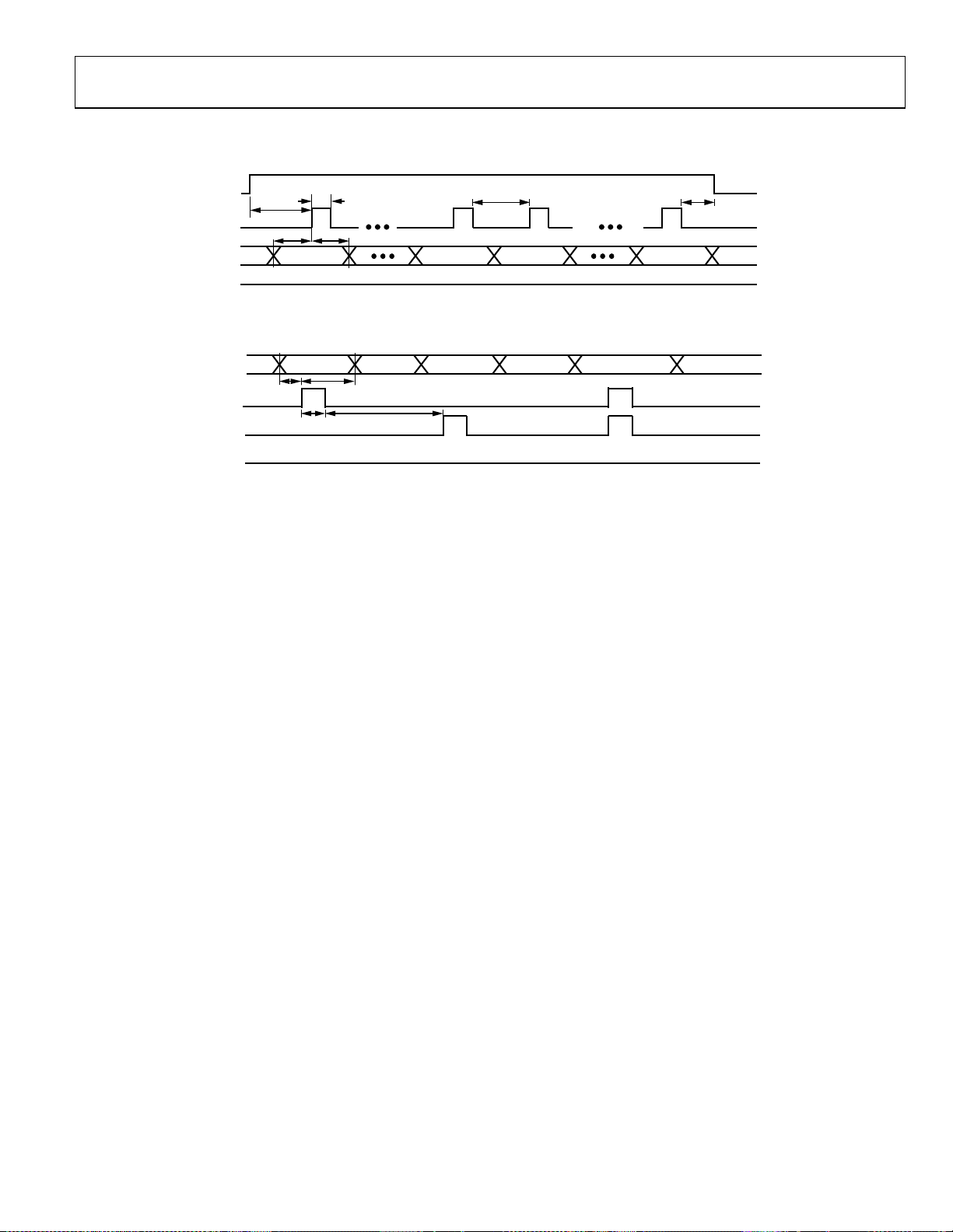
PARALLEL AND SERIAL INTERFACE TIMING
CS
SCLK
SDAT
SENB
t
2
t
1
t
t
5
6
B-LSB B-MSB A-LSBX
t
3
ALWAYS HIG H
A-MSB
t
4
X
07584-003
Figure 2. SPI Port Timing Diagram
BIT[5:0]
DENA
DENB
SENB
GAIN A GAIN B
t
t
10
9
t
7
t
8
ALWAYS LOW
Figure 3. Parallel Port Timing Diagram
GAIN A, GAIN B
07584-004
Rev. A | Page 5 of 28
AD8366
ABSOLUTE MAXIMUM RATINGS
Table 2.
Parameter Rating
Supply Voltages, VPSIx and VPSOx 5.5 V
ENBL, SENB, DENA, DENB, BIT0, BIT1, BIT2,
BIT3, BIT4, BIT5
IPPA, IPMA, IPPB, IPMB 5.5 V
OPPA, OPMA, OPPB, OPMB 5.5 V
OFSA, OFSB 5.5 V
DECA, DECB, VCMA, VCMB, CCMA, CCMB 5.5 V
Internal Power Dissipation 1.4 W
θJA (With Pad Soldered to Board) 45.4°C/W
Maximum Junction Temperature 150°C
Operating Temperature Range −40°C to +85°C
Storage Temperature Range −65°C to +150°C
Lead Temperature (Soldering, 60 sec) 300°C
5.5 V
Stresses above those listed under Absolute Maximum Ratings
may cause permanent damage to the device. This is a stress
rating only; functional operation of the device at these or any
other conditions above those indicated in the operational
section of this specification is not implied. Exposure to absolute
maximum rating conditions for extended periods may affect
device reliability.
ESD CAUTION
Rev. A | Page 6 of 28
AD8366
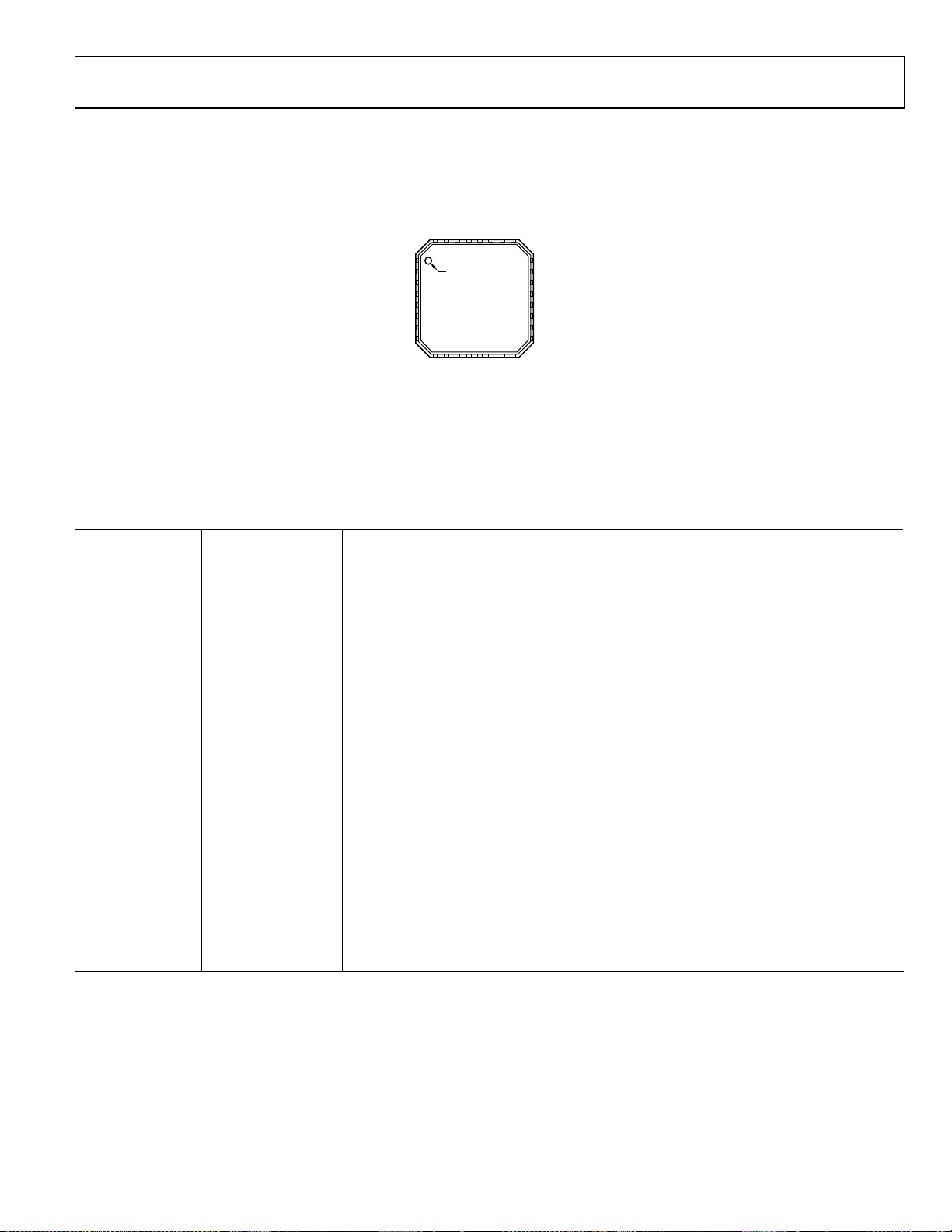
PIN CONFIGURATION AND FUNCTION DESCRIPTIONS
DECA
OFSA
CCMA
VCMA
VPSOAOPPA
OPMA
SENB
29
28
27
26
31
30
32
1
VPSIA
IPPA
IPMA
ENBL
ICOM
IPMB
IPPB
VPSIB
NOTES
1. THE EXPOSED PAD MUST BE CONNECTED
TO GROUND.
2
3
4
5
6
7
8
PIN 1
INDICATOR
AD8366
TOP VIEW
(Not to Scale)
9
11
10
OFSB
DECB
CCMB
Figure 4. Pin Configuration
Table 3. Pin Function Descriptions
Pin No. Mnemonic Description
1, 8, 13, 28
VPSIA, VPSIB, VPSOB,
Input and Output Stage Positive Supply Voltage (4.75 V to 5.25 V).
VPSOA
2, 3, 6, 7
IPPA, IPMA, IPMB,
Differential Inputs.
IPPB
4 ENBL Chip Enable. Pull this pin high to enable.
5, 20 ICOM, OCOM
Input and Output Ground Pins. Connect these pins via the lowest possible impedance to
ground.
9, 32 DECB, DECA
/2 Reference Decoupling Node. Connect a decoupling capacitor from these nodes to
V
POS
ground.
10, 31 OFSB, OFSA
Output Offset Correction Loop Compensation. Connect a capacitor from these nodes to
ground to enable the correction loop. Tie this pin to ground to disable.
11, 30 CCMB, CCMA Connect These Nodes to Ground.
12, 29 VCMB, VCMA
Output Common-Mode Setpoint. These pins default to V
from a low impedance source to change the output common-mode voltage.
14, 15, 26, 27
OPPB, OPMB, OPMA,
Differential Outputs.
OPPA
16, 17 DENB, DENA
Data Enable. Pull these pins high to address each or both channels for parallel gain
programming. These pins are not used in serial mode.
18, 19, 21, 22, 23, 24
25 SENB
BIT5, BIT4, BIT3,
BIT2/SCLK, BIT1/SDAT,
BIT0/CS
Parallel Data Path (When SENB Is Low). When SENB is high, BIT0 becomes a chip select (CS),
BIT1 becomes a serial data input (SDAT ), and BIT2 becomes a serial clock (SCLK). BIT3 to BIT5
are not used in serial mode.
Serial Interface Enable. Pull this pin high for serial gain programming mode and pull this pin low
for parallel gain programming mode.
EPAD The exposed pad must be connected to ground.
25
BIT0/CS
24
BIT1/SDAT
23
BIT2/SCLK
22
BIT3
21
OCOM
20
BIT4
19
BIT5
18
DENA
17
12
13
14
15
16
OPPB
DENB
VCMB
OPMB
VPSOB
07584-028
/2 if left open. Drive these pins
POS
Rev. A | Page 7 of 28
AD8366
A
A
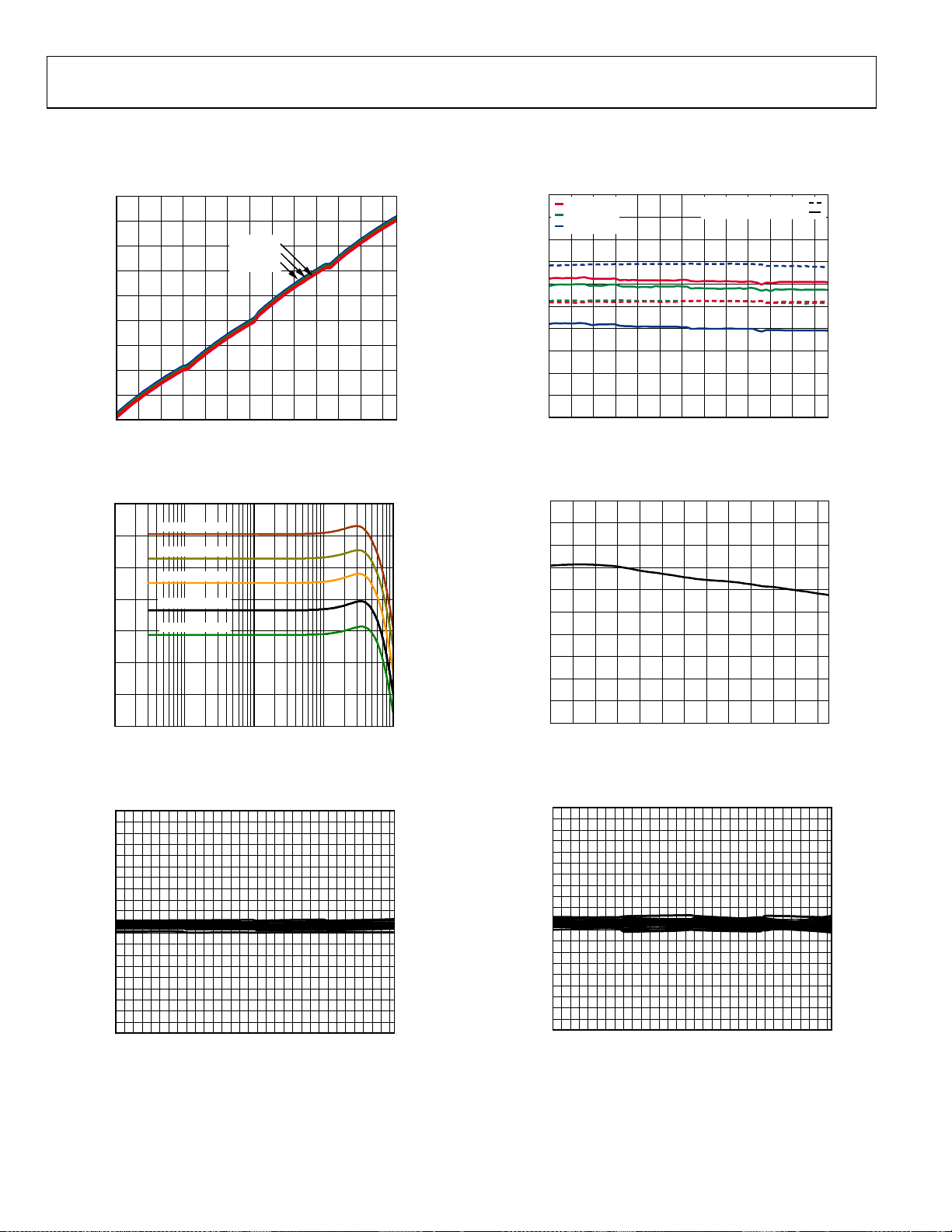
TYPICAL PERFORMANCE CHARACTERISTICS
VS = 5 V, TA = 25°C, ZS = 200 Ω, ZL = 200 Ω, f = 10 MHz, unless otherwise noted.
22
20
18
16
14
12
GAIN (dB)
10
8
6
4
0 5 10 15 20 25 30 35 40 45 50 55 60
TA = +85°C
= +25°C
T
A
= –40°C
T
A
GAIN CODE
Figure 5. Gain vs. Gain Code at 500 kHz, 3 MHz, 10 MHz, and 50 MHz
25
20
15
10
5
0
5
GAIN CHANNEL A, GAIN CHANNEL B (dB)
–10
100k 1M 10M 100M 1G
GAIN CODE 63
GAIN CODE 48
GAIN CODE 32
GAIN CODE 16
GAIN CODE 00
FREQUENCY ( Hz)
Figure 6. Frequency Response vs. Gain Code
1.0
0.9
0.8
0.7
0.6
0.5
0.4
0.3
TCH (dB)
0.2
0.1
0
–0.1
–0.2
–0.3
–0.4
–0.5
AMPLITUDE MISM
–0.6
–0.7
–0.8
–0.9
–1.0
0 102030405060
GAIN CODE
Figure 7. Channel A-to-Channel B Amplitude Mismatch vs. Gain Code,
2 V p-p Output
07584-005
07584-007
07584-008
0.5
TA = +85°C
= +25°C
T
A
0.4
0.3
0.2
0.1
–0.1
GAIN ERROR (dB)
–0.2
–0.3
–0.4
–0.5
= –40°C
T
A
0
0 5 10 15 20 25 30 35 40 45 50 55 60
FREQUENCY = 3MHz
FREQUENCY = 50MHz
GAIN CODE
Figure 8. Gain Error vs. Gain Code, Error Normalized to 10 MHz
21.0
20.8
20.6
20.4
20.2
20.0
GAIN (dB)
19.8
19.6
19.4
19.2
19.0
–40 –30 –20 –10 0 10 20 30 40 50 60 70 80
TEMPERATURE (°C)
Figure 9. Gain vs. Temperature at Maximum Gain at 10 MHz
1.0
0.9
0.8
0.7
0.6
0.5
0.4
0.3
0.2
0.1
TCH (Degrees)
0
–0.1
–0.2
–0.3
–0.4
–0.5
PHASE MISM
–0.6
–0.7
–0.8
–0.9
–1.0
0 102030405060
GAIN CODE
Figure 10. Channel A-to-Channel B Phase Mismatch vs. Gain Code,
2 V p-p Output
07584-006
07584-017
07584-009
Rev. A | Page 8 of 28
AD8366
20
TA = +85°C
T
= +25°C
A
18
T
= –40°C
A
16
14
12
10
8
OP1dB (dBm)
6
4
2
0
0 5 10 15 20 25 30 35 40 45 50 55 60
GAIN CODE
20
18
16
14
12
10
8
6
4
2
0
Figure 11. OP1dB vs. Gain Code at 500 kHz, 3 MHz, 10 MHz, and 50 MHz
50
45
40
35
30
25
OIP3 (dBm)
20
15
10
TA = +85°C
5
T
= +25°C
A
T
= –40°C
A
0
0 5 10 15 20 25 30 35 40 45 50 55 60
FREQUENCY = 10MHz
FREQUENCY = 50MHz
GAIN CODE
60
55
50
45
40
35
30
25
20
15
10
Figure 12. OIP3 vs. Gain Code at 10 MHz and 50 MHz Frequency, 2 V p-p
Composite Output
0
TA = +85°C
= +25°C
T
–10
A
= –40°C
T
A
–20
–30
–40
–50
–60
IMD3 (dBc)
–70
–80
–90
–100
–110
0 5 10 15 20 25 30 35 40 45 50 55 60
GAIN CODE
FREQUENCY = 10MHz
FREQUENCY = 50MHz
Figure 13. Two-Tone Output IMD3 vs. Gain Code at 10 MHz and 50 MHz
Frequency, 2 V p-p Composite Output
20
TA = +85°C
T
= +25°C
A
18
T
= –40°C
A
16
14
12
10
8
OP1dB ( dBVrms)
07584-030
OP1dB (dBm)
6
4
2
0
0 102030405060708090100110120130140150
FREQUENCY ( MHz)
GAIN CODE 0
GAIN CODE 63
Figure 14. OP1dB vs. Frequency at Gain Code 0 and Gain Code 63
50
45
40
35
30
25
OIP3 (dBm)
OIP3 (dBVrms)
07584-039
20
15
10
TA = +85°C
5
T
= +25°C
A
T
= –40°C
A
0
0 10 20 30 40 50 60 70 80 90 100 110 120 130 140 150
FREQUENCY (M Hz)
GAIN CODE 63
GAIN CO DE 0
GAIN CO DE 32
CHANNEL A
CHANNEL B
Figure 15. OIP3 vs. Frequency, Gain Code 0, Gain Code 32, and Gain Code 63,
2 V p-p Composite Output
TA = +85°C
T
= +25°C
A
–10
T
= –40°C
A
–30
–50
IMD3 (dBc)
–70
–90
–110
10 20 30 40 50 60 70 80 90 100 110 120 130 140 150
07584-042
Figure 16. Two-Tone Output IMD3 vs. Frequency at Gain Code 0,
GAIN CODE 0
GAIN CODE 63
FREQUENC Y (MHz)
CHANNEL A
CHANNEL B
GAIN CODE 32
Gain Code 32, and Gain Code 63, 2 V p-p Composite Output
20
18
16
14
12
10
8
OP1dB (d BVrms)
6
4
2
0
07584-041
07584-040
07584-029
Rev. A | Page 9 of 28

AD8366
100
90
80
70
60
50
OIP2 (dBm)
40
30
20
TA = +85°C
10
T
= +25°C
A
T
= –40°C
A
0
0 5 10 15 20 25 30 35 40 45 50 55 60
FREQUENCY = 10M Hz
FREQUENCY = 50M Hz
GAIN CODE
Figure 17. OIP2 vs. Gain Code at 10 MHz and 50 MHz Frequency,
2 V p-p Composite Output
0
TA = +85°C
= +25°C
T
A
IMD2 (dBc)
–10
–20
–30
–40
–50
–60
–70
–80
–90
–100
= –40°C
T
A
0 5 10 15 20 25 30 35
FREQUENCY = 10MHz
FREQUENCY = 50MHz
GAIN CODE
45 50 55 60
40
Figure 18. Two-Tone Output IMD2 vs. Gain Code at 10 MHz and 50 MHz
Frequency, 2 V p-p Composite Output
0
GAIN CODE 0
–10
GAIN CODE 32
GAIN CODE 63
–20
–30
–40
–50
–60
–70
HD2, HD3 (dBc)
–80
–90
–100
–110
–120
1 10 100 1000
FREQUENCY (MHz)
Figure 19. Harmonic Distortion vs. Frequency at Gain Code 0, Gain Code 32,
and Gain Code 63, 2 V p-p Output
HD2
HD3
100
90
80
70
60
50
40
30
20
10
0
100
90
80
70
60
50
OIP2 (dBm)
OIP2 (dBVrms)
07584-044
40
30
20
TA = +85°C
10
T
= +25°C
A
T
= –40°C
A
0
10 20 30 40 50 60 70 80 90 100 110 120 130 140 150
FREQUENCY (MHz)
GAIN CODE 63
GAIN CODE 0
CHANNEL A
CHANNEL B
07584-043
Figure 20. OIP2 vs. Frequency at Gain Code 0 and Gain Code 63, 2 V p-p
Composite Output
0
TA = +85°C
T
= +25°C
–10
A
T
= –40°C
A
–20
–30
–40
–50
IMD2 (dBc)
–60
–70
–80
–90
–100
0 102030405060708090100110120130140150
07584-045
FREQUENCY ( MHz)
CHANNEL A
CHANNEL B
GAIN CODE 0
GAIN CODE 63
07584-052
Figure 21. Two-Tone Output IMD2 vs. Frequency,
Gain Code 0 and Gain Code 63, 2 V p-p Composite Output
0
TA = +85°C
= +25°C
T
–10
A
= –40°C
T
A
–20
–30
–40
–50
–60
–70
–80
HD2, GAIN CO DE 0 (dBc)
–90
–100
–110
1.0 1.2 1.4 1.6 1.8 2.0 2.2 2.4 2.6 2.8 3.0
07584-032
Figure 22. HD3/HD2 vs. V
VCMA, VCMB (V)
at 10 MHz, Gain Code 0, 2 V p-p Output
OCM
CHANNEL A
CHANNEL B
0
–10
–20
–30
–40
–50
–60
–70
–80
–90
–100
HD3, GAIN CO DE 0 (dBc)
07584-023
Rev. A | Page 10 of 28

AD8366
–
–
60
50
40
30
OIP3 (dBm)
20
10
TA = +85°C
= +25°C
T
A
= –40°C
T
A
0
–3 –2 –1 0 1 2 3 4 5
P
Figure 23. OIP3 vs. Output Power (P
Codes, 10 MHz Frequency
100
90
80
70
60
50
OIP2 (dBm)
40
30
20
TA = +85°C
10
T
= +25°C
A
T
= –40°C
A
0
–8–7–6–5–4–3–2–1012345
P
Figure 24. OIP2 vs. Output Power (P
Codes, 10 MHz Frequency
60
TA = +85°C
= +25°C
T
A
HD2 (dBc)
–65
–70
–75
–80
–85
–90
–95
–100
–105
–110
= –40°C
T
A
–5–4–3–2–1012345678
Figure 25. HD2 vs. Output Power (P
10 MHz Frequency
GAIN CODE 0
GAIN CODE 63
PER TONE (dBm)
OUT
) at Minimum and Maximum Gain
OUT
GAIN CODE 0
GAIN CODE 63
PER TONE (dBm)
OUT
) at Minimum and Maximum Gain
OUT
GAIN CO DE 0
GAIN CO DE 63
P
(dBm)
OUT
) at Gain Code 0 and Gain Code 63,
OUT
0
TA = +85°C
T
= +25°C
A
–10
T
= –40°C
A
–20
–30
–40
–50
–60
IMD3 (dBc)
–70
–80
–90
–100
–110
–3–2–1012345
P
PER TONE (dBm)
07584-055
Figure 26. IMD3 vs. Output Power (P
OUT
OUT
GAIN CODE 0
GAIN CODE 63
) at Minimum-to-Maximum Gain
07584-061
Codes, 10 MHz Frequency
0
TA = +85°C
T
= +25°C
A
–10
T
= –40°C
A
–20
–30
–40
–50
IMD2 (dBc)
–60
–70
–80
–90
–100
–8 –7 –6 –5 –4 –3 –2 –1 0 1 2 3 4 5
P
PER TONE (dBm)
07584-060
Figure 27. IMD2 vs. Output Power (P
OUT
OUT
GAIN CODE 0
GAIN CODE 63
07584-062
) at Minimum and Maximum Gain
Codes, 10 MHz Frequency
60
TA = +85°C
T
= +25°C
A
–65
–70
–75
–80
–85
–90
–95
HD3 (dBc)
–100
–105
–110
–115
–120
07584-053
Figure 28. HD3 vs. Output Power (P
= –40°C
T
A
–5 –4 –3 –2 –1 0 1 2 3 4 5
P
(dBm)
OUT
) for Gain Code 0 and Gain Code 63,
OUT
GAIN CODE 0
GAIN CODE 63
07584-054
10 MHz Frequency
Rev. A | Page 11 of 28

AD8366
A
√
300
TA = +85°C
T
280
260
240
220
200
180
160
SUPPLY CURRENT (mA)
140
120
100
= +25°C
A
T
= –40°C
A
0 5 10 15 20 25 30 35 40 45 50 55 60
GAIN CODE
07584-038
Figure 29. Supply Current vs. Gain Code at 10 MHz
30
CHANNEL B, FREQUENCY = 0.5MHz
CHANNEL A, FREQUENCY = 0.5MHz
28
CHANNEL B, FREQUENCY = 3MHz
CHANNEL A, FREQUENCY = 3MHz
26
CHANNEL B, FREQUENCY = 10MHz
CHANNEL A, FREQUENCY = 10MHz
CHANNEL B, FREQUENCY = 50MHz
24
CHANNEL A, FREQUENCY = 50MHz
22
20
18
NOISE FIG URE (dB)
16
14
12
10
0 5 10 15 20 25 30 35 40 45 50 55 60
IN
A
G
E
D
O
C
07584-011
Figure 30. Noise Figure vs. Gain Code at 0.5 MHz, 3 MHz, 10 MHz, and 50 MHz
280
CHANNEL A: RIN, GAIN CODE 0
CHANNEL A: RIN, GAIN CODE 63
270
CHANNEL B: RIN, GAIN CODE 32
CHANNEL A: CIN, GAIN CODE 0
260
CHANNEL A: CIN, GAIN CODE 63
CHANNEL B: CIN, GAIN CODE 32
CHANNEL A: RIN, GAIN CODE 32
250
CHANNEL A: RIN, GAIN CODE 0
CHANNEL B: RIN, GAIN CODE 63
240
230
220
210
INPUT RESISTANCE (Ω)
200
CHANNEL A: CIN, GAIN CODE 32
190
CHANNEL B: CIN, GAIN CODE 0
CHANNEL B: CIN, GAIN CODE 63
180
0 20 40 60 80 100 120 140 160 180 200
FREQUENCY (MHz)
3.0
2.7
2.4
2.1
1.8
1.5
1.2
0.9
0.6
0.3
0
INPUT CAPACITANCE (pF)
Figure 31. Differential Parallel Input Resistance and Capacitance vs.
Frequency
60
CHANNEL A
CHANNEL B
55
GAIN CODE 63
Hz)
50
GAIN CODE 47
GAIN CODE 48
GAIN CODE 31
45
GAIN CODE 32
GAIN CODE 15
40
GAIN CODE 16
GAIN CODE 0
35
L DENSITY (nV/
30
25
20
NOISE SPECTR
15
10
0.1 1 10 100 1000
FREQUENCY (kHz)
07584-010
Figure 32. Noise Spectral Density vs. Frequency
30
28
GAIN CODE 0
GAIN CODE 15
26
GAIN CODE 16
GAIN CODE 31
24
GAIN CODE 32
GAIN CODE 47
GAIN CODE 48
22
GAIN CODE 63
20
18
NOISE FIGURE (dB)
16
14
12
10
0.1 1 10 100 1000
FREQUENCY (kHz )
CHANNEL A
CHANNEL B
07584-012
Figure 33. Noise Figure vs. Frequency
40
CHANNEL A: R
CHANNEL A: R
37
CHANNEL B: R
CHANNEL A: L
CHANNEL A: L
34
CHANNEL B: L
CHANNEL A: R
31
CHANNEL A: R
28
25
22
19
OUTPUT RESI STANCE (Ω)
16
CHANNEL B: R
CHANNEL A: L
13
CHANNEL B: L
CHANNEL B: L
10
0 20 40 60 80 100 120 140 160 180 200
07584-013
, GAIN CODE 0
OUT
, GAIN CODE 63
OUT
, GAIN CODE 32
OUT
, GAIN CODE 0
OUT
, GAIN CODE 63
OUT
, GAIN CODE 32
OUT
, GAIN CODE 32
OUT
, GAIN CODE 0
OUT
, GAIN CODE 63
OUT
, GAIN CODE 32
OUT
, GAIN CODE 0
OUT
, GAIN CODE 63
OUT
FREQUENCY ( MHz)
7.5
7.2
6.9
6.6
6.3
6.0
5.7
5.4
5.1
4.8
4.5
OUTPUT INDUCTNACE (nH)
07584-014
Figure 34. Differential Series Output Resistance and Inductance vs.
Frequency
Rev. A | Page 12 of 28

AD8366
A
0
PSRR GAIN CODE 0
PSRR GAIN CODE 63
–10
–20
–30
–40
–50
PSRR (dB)
–60
–70
–80
–90
10 20 30 40 50 60 70 80 90 100 110 120 130 140 150
FREQUENCY ( MHz)
Figure 35. Power Supply Rejection Ratio (PSRR) vs. Frequency
2.0
GAIN CODE 32
GAIN CODE 0
1.8
GAIN CODE 63
1.6
1.4
1.2
Y (ns)
1.0
0.8
GROUP DEL
0.6
0.4
0.2
0
10 20 30 40 50 60 70 80 90 100 110 120 130 140 150
FREQUENCY ( MHz)
Figure 36. Group Delay vs. Frequency at Gain Code 0, Gain Code 32, and
Gain Code 63
0
MEASURED CHANNEL AT GAIN CODE 63
MEASURED CHANNEL AT GAIN CODE 32
MEASURED CHANNEL AT GAIN CODE 0
–20
–40
07584-036
07584-021
140
130
120
110
100
90
80
70
60
SFDR (dB)
50
40
30
20
TA = +85°C
T
= +25°C
A
10
T
= –40°C
A
0
0 5 10 15 20 25 30 35 40 45 50 55 60
GAIN CODE
FREQUENCY = 10M Hz
FREQUENCY = 50M Hz
Figure 38. SFDR vs. Gain Code at 10 MHz and 50 MHz,
1 Hz Analysis Bandwidth
90
GAIN CODE 63
80
70
60
50
40
CMRR (dB)
30
20
10
0
1M 10M 100M 1G
FREQUENCY (Hz)
GAIN CODE 32
GAIN CODE 0
Figure 39. Common-Mode Rejection Ratio (CMRR) vs. Frequency
0
PIN = +10dBm
P
= +5dBm
IN
P
–20
–40
–60
= 0dBm
IN
P
= –5dBm
IN
P
= –10dBm
IN
07584-037
7584-016
–60
ISOLATION (dB)
–80
–100
–120
1 10 100 1000
DRIVEN CHANNEL AT GAIN CODE 0
FREQUENCY ( MHz)
Figure 37. Channel-to-Channel Isolation vs. Frequency,
Channel A Driven, Channel B Measured
07584-034
–80
–100
–120
FORWARD LEAKAGE (dBm)
–140
–160
1 10 100 1000
FREQUENCY ( MHz)
Figure 40. Forward Leakage vs. Frequency, Part Disabled
07584-031
Rev. A | Page 13 of 28

AD8366
1.2
1.0
0.8
0.6
0.4
0.2
0
–0.2
–0.4
OUTPUT VOLTAGE (V)
–0.6
–0.8
–1.0
–1.2
–5–4–3–2–1012345
0pF
TIME (ns)
10pF
07584-067
Figure 41. Large Signal Pulse Response, Gain Code 0, Input Signal 1.2 V p-p,
0 pF and 10 pF Capacitive Loading Conditions
1.4
1.2
1.0
0.8
0.6
0.4
0.2
0
–0.2
–0.4
OUTPUT VOLTAGE (V)
–0.6
–0.8
–1.0
–1.2
–5–4–3–2–1012345
TIME (ns)
0pF
10pF
07584-068
Figu re 44. Large Signal Pulse Respon se, Gain Code 63, Input Signal 240 mV p-p,
0 pF and 10 pF Capacitive Loading Conditions
1
2
3
ΩΩ
CH1 1V CH2 100mV M1µs
T 4.02µs
Figure 42. ENBL Time Domain Response
0
–20
–40
–60
S12 MAG (dB)
–80
–100
–120
0.1 1 10 100 1000
FREQUENCY ( MHz)
5GS/s
100k pts
A CH1 1.60V
07584-065
CH3 50mV CH4 1VΩΩ
M 200ns 250MS/s 4.0ns/pt A CH4 2.48V
07584-064
Figure 45. Gain Step Time Domain Response, Minimum-to-Maximum Gain
(Time Scale 200 ns/division), CH4 = Digital Control Inputs
07584-033
Figure 43. Reverse Isolation (S12) vs. Frequency
Rev. A | Page 14 of 28

AD8366
V
V
A
V
CIRCUIT DESCRIPTION
The AD8366 is a dual, differential, digitally controlled VGA
with 600 MHz of 3 dB bandwidth and a gain range of 4.5 dB to
20.25 dB adjustable in 0.25 dB steps. Using a proprietary variable
gain architecture, the AD8366 is able to achieve excellent linearity
(45 dBm) and noise performance (11.7 nV/√Hz) at 10 MHz at
minimum gain. Intended for use in direct conversion systems, the
part also includes dc offset correction that can be disabled easily
by grounding either OFSA or OFSB. In addition, the part offers
an adjustable output common-mode range of 1.6 V to 3 V.
The main signal path is shown in Figure 46. It consists of an
input transconductance, a variable-gain cell, and an output
transimpedance amplifier.
ARIABLE
INM
INP
100Ω
100Ω
CURRENT-GAIN
STAGE
I
VIRTUAL
GROUND
Figure 46. Main Signal Path
OUTPUT
BUFFER
ZA
VIRTUAL
GROUND
12.5Ω
12.5Ω
OUTP
OUTM
7584-071
The input transconductance provides a broadband 200 Ω
differential termination and converts the input voltage to a
current. This current is fed into the variable current-gain cell.
The output of this cell goes into the transimpedance stage, which
generates the output voltage. The transimpedance is fixed at 500 Ω,
with a roughly 25 Ω differential output impedance.
INPUTS
The inputs to the digitally-controlled VGAs in the AD8366 are
differential and can be either ac- or dc-coupled. The AD8366
synthesizes a 200 Ω (differential) input impedance, with a return
loss (re: 200 Ω) of better than 10 dB to 200 MHz. The nominal
common-mode input voltage to the part is V
/2, but the AD8366
POS
can be dc-coupled to parts with lower common modes if these
parts can sink current. The amount of current sinking required
depends on the input common-mode level and is given by
I
(per leg) = (V
SINK
The input common-mode range is 1.5 V to V
POS
/2 − V
ICM
)/100
POS
/2.
OUTPUTS
The outputs of the digitally-controlled VGAs are differential and
can be either ac- or dc-coupled. The AD8366 synthesizes a 25 Ω
differential output impedance, with a return loss (re: 25 Ω) of
better than 10 dB to 120 MHz. The nominal common-mode
output voltage is V
driving the VCMA or VCMB pins.
/2; however, it can be lowered or raised by
POS
OUTPUT DIFFERENTIAL OFFSET CORRECTION
To prevent significant levels of offset from appearing at the
outputs of the AD8366, each digitally controlled VGA has a
differential offset correction loop, as shown in Figure 47. This
loop senses any differential offset at the output and corrects for
it by injecting an opposing current at the input differential ground.
The loop is able to correct for input dc offsets of up to ±20 mV.
Because the loop automatically nulls out any dc or low frequency
offset, the effect of the loop is to introduce a high-pass corner into
the transfer function of the digitally controlled VGA. The
location of this high-pass corner depends on both the gain
setting and the value of the capacitor connected to the OFSx pin
(OFSA for DVGA A and OFSB for DVGA B) and is given by
GC
=
()
()
C
()
kHz
f
,3
HPdB
OFS
40001.0374300
+
102π
+
where:
GC is the gain code (a value from 0 to 63).
is the value of the capacitance connected to OFSA or OFSB,
C
OFS
in picofarads (pF).
The offset correction loop can be disabled by grounding either
OFSA or OFSB.
RIABLE-GAI N
STAGE
I
INP
INM
Figure 47. Differential Offset Correction Loop
g
m2
C
g
OFS
m1
OUTPUT
BUFFER
ZA
OFFSET
COMPENSATI ON
LOOP
OUTP
OUTM
07584-073
OUTPUT COMMON-MODE CONTROL
To interface to ADCs that require different input common-mode
voltages, the AD8366 has an adjustable output common-mode
level. The output common-mode level is normally set to V
however, it can be changed between 1.6 V and 3 V by driving
the VCMA pin or the VCMB pin. The input equivalent circuit
for the VCMA pin is shown in Figure 48; the VCMB pin has the
same input equivalent circuit.
4kΩ
/2
POS
500Ω
VCMA
07584-072
Figure 48. Input Equivalent Circuit for VCMA
POS
/2;
Rev. A | Page 15 of 28

AD8366
GAIN CONTROL INTERFACE
The AD8366 provides two methods of digital gain control:
serial or parallel. When the SENB pin is pulled low, the part
is in parallel gain control mode. In this mode, the two digitally
controlled VGAs can be programmed simultaneously, or one at
a time, depending on the levels at DENA and DENB. If the SENB
pin is pulled high, the part is in serial gain control mode, with
Pin 24, Pin 23, and Pin 22 corresponding to the CS, SDAT, and
SCLK signals, respectively.
The voltage gain of the AD8366 is well approximated by
Gain (dB) = GainCode × 0.253 + 4.5
Note that at several major transitions (15 to 16, 31 to 32, and 47 to
48), the gain changes significantly less (0 dB step) or significantly
more (0.5 dB step) than the desired 0.25 dB step. This is inherent
in the design of the part and is related to the partitioning of the
variable gain block into a fine-gain and a coarse-gain section.
25.0
22.5
20.0
17.5
15.0
12.5
GAIN (dB)
10.0
7.5
5.0
2.5
0
0 5 10 15 20 25 30 35 40 45 50 55 60
GAIN CODE
Figure 49. Gain and Gain Step Error vs. Gain Code at 10 MHz
1.0
0.8
0.6
0.4
0.2
0
–0.2
–0.4
–0.6
–0.8
–1.0
GAIN STEP ERROR (dB)
07584-063
Rev. A | Page 16 of 28

AD8366
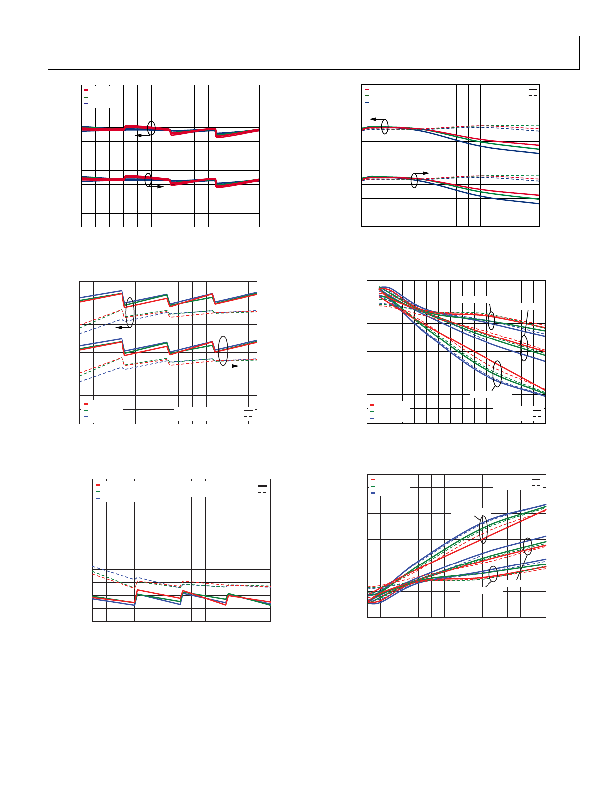
APPLICATIONS INFORMATION
BASIC CONNECTIONS
Figure 50 shows the basic connections for operating the AD8366.
A voltage from 4.75 V to 5.25 V should be applied to the supply
pins. Each supply pin should be decoupled with at least one low
inductance, surface-mount ceramic capacitor of 0.1 µF placed as
close as possible to the device.
The differential input impedance is 200 Ω and sits at a nominal
common-mode voltage of V
or ac-coupled. If using direct dc coupling, the common-mode
voltage, V
, can range from 1.5 V to V
CM
/2. The inputs can be dc-coupled
POS
/2.
POS
The output buffers of the AD8366 are low impedance around
25 Ω designed to drive ADC inputs. The output common-mode
voltage defaults to V
/2; however, it can be adjusted by applying a
POS
desired external voltage to VCMA/VCMB. The common-mode
voltage can be adjusted from 1.6 V to 3.0 V without significant
harmonic distortion degradation.
To enable the AD8366, the ENBL pin must be pulled high. Taking
ENBL low disables the device, reducing current consumption to
approximately 3 mA at ambient temperature.
VPOS
0.01µF
8200pF
0.01µF
CHANNEL A
OUTPUT
0.01µF
VPSIA
IPPA
IPMA
ENBL
ICOM
IPMB
IPPB
VPSIB
0.01µF
0.01µF
8200pF
OFSA
DECA
ECB
D
OFSB
A
VCMA
CCM
VPSOA
AD8366
CCMB
VCMB
VPSOB
VPOS
PPA
O
OPMA
BIT0/CS
BIT1/SDAT
BIT2/SCLK
OPPB
OPMB
0.01µF
0.01µF
SENB
OCOM
DENA
DENB
BIT3
BIT4
BIT5
PARALLEL/SERIAL
CHANNEL B
OUTPUT
CONTROL I NTERFACE (PCI )
07584-046
CHANNEL A
INPUT
VPOS
CHANNEL B
INPUT
VPOS
0.1µF 0.1µF
0.1µF 0.1µF
VPOS
0.1µF 0.1µF
Figure 50. Basic Connections
Rev. A | Page 17 of 28

AD8366
PAD
FILTER
BALUN
RF
ADL5523
MATCHI NG
NETWORK
ADL5523
Figure 51. Direct Conversion Receiver Block Diagram
DIRECT CONVERSION RECEIVER DESIGN
A direct conversion receiver directly demodulates an RF modulated
carrier to baseband frequencies, where the signals can be detected
and the conveyed information recovered. Eliminating the IF
stages and directly converting the signal to effectively zero IF
results in reduced component count. The image problems
associated with the traditional superheterodyne architectures
can be ignored as well. However, there are different challenges
associated with direct conversion that include LO leakage, dc
offsets, quadrature imperfections, and image rejection. LO
leakage causes self mixing that results in squaring of the LO
waveform which generates a dc offset that falls in band for the
direct conversion receiver. Residual dc offsets create a similar
interfering signal that falls in band. I/Q amplitude and phase
mismatch lead to degraded SNR performance and poor image
rejection in the direct conversion system. Figure 51 shows the
block diagram for a direct conversion receiver system.
LC LOW-
PASS
FILTER
0
90
ADL5380 AD8366
LO
ADF4350
LC LOW-
PASS
FILTER
The image rejection ratio is the ratio of the intermediate frequency
(IF) signal level produced by the desired input frequency to that
produced by the image frequency. The image rejection ratio is
expressed in decibels (dB). Appropriate image rejection is critical
because the image power can be much higher than that of the
desired signal, thereby plaguing the downconversion process.
Amplitude and phase balance between the I/Q channels are
critical for high levels of image rejection. Image rejection of
greater than 47 dB was measured for the combined ADL5380
and the AD8366 for a 5 MHz baseband frequency, as seen in
Figure 53. This level of image rejection corresponds to a ±0.5°
phase mismatch and a ±0.05 dB of amplitude mismatch for the
combined ADL5380 and AD8366. Looking back to Figure 7 and
Figure 10, the AD8366 exhibits only ±0.05 dB of amplitude mismatch
o
and ±0.05
of phase mismatch, thus implying that the AD8366
does not introduce additional amplitude and phase imbalance.
55
LC LOW-
PASS
FILTER
LC LOW-
PASS
FILTER
TO
ADC
07584-047
QUADRATURE ERRORS AND IMAGE REJECTION
An overall RF-to-baseband EVM performance was measured
with the ADL5380 IQ demodulator preceding the AD8366, as
shown in Figure 56. In this setup, no LC low-pass filters were used
between the ADL5380 and AD8366. A 1900 MHz W-CDMA RF
signal with a 3.84 MHz symbol rate was used. The local oscillator
(LO) is set at 1900 MHz to obtain a zero IF baseband signal.
The gain of the AD8366 is set to maximum gain (~20.25 dB).
Figure 52 shows the SNR vs. the input power of the cascaded
system for a 5 MHz analysis bandwidth. The broad input power
range over which the system exhibits strong SNR performance
reflects the superior dynamic range of the AD8366.
45
40
35
30
25
20
SNR (dB)
15
10
5
0
–75 –65 –55 –45 –35 –25 –15 –5 5
INPUT POW ER (dBm)
Figure 52. SNR vs. RF Input Power Level
07584-048
Rev. A | Page 18 of 28
50
45
40
35
IMAGE REJECTI ON (dB)
30
25
900 150013001100 1700 1900 2100 2300 2500 2700
RF FREQUENCY (MHz)
Figure 53. Image Rejection vs. RF Frequency
2900
07584-049

AD8366
–
LOW FREQUENCY IMD3 PERFORMANCE
To measure the IMD3 data at low frequencies, wideband
transformer baluns from North Hills Signal Processing Corp.
were used, specifically the 0301BB and the 0520BB. Figure 55
shows the IMD3 performance vs. frequency for a 2 V p-p
composite output. The IMD3 performance was also measured
for the combined ADL5380 and AD8366 system, as shown in
Figure 56, with an FFT spectrum analyzer. An FFT spectrum
analyzer works very similar to a typical ADC, the input signal
is digitized at a high sampling rate that is then passed through an
antialiasing filter. The resulting signal is transformed to the
frequency domain using fast Fourier transforms (FFT).
The single-ended RF signal from the source generator is converted
to a differential signal using a balun that gets demodulated and
down converted to differential IF signals through the ADL5380.
This differential IF signal drives the AD8366, thus eliminating
the need for low frequency baluns. Figure 54 shows the IMD3
performance vs. frequency over the 500 kHz to 5 MHz range
for minimum and maximum gain code setting on the AD8366.
During the measurements, the output was set to 2 V p-p composite.
20
GC63
GC0
–30
–40
–50
–60
IMD3 (dBc)
–70
–80
–90
0.5 1.0 1.5 2.0 2.5 3.0 3.5 4.0 4.5 5.0
FREQUENC Y (MHz)
Figure 54. System IMD3 vs. Frequency, 2 V p-p Composite at
the Output of the AD8366
50
FREQUENCY = 1MHz
FREQUENCY = 3MHz
45
40
35
30
25
20
OIP3 (dBm)
15
10
5
0
0 5 10 15 20 25 30 35 40 45 50 55 60
GAIN CODE
Figure 55. OIP3 on Low Frequency, 2 V p-p Composite
0
–10
–20
–30
–40
–50
–60
–70
–80
–90
–100
07584-018
IMD3 (dBc)
07584-035
Rev. A | Page 19 of 28

AD8366
V
VPOS
0.1µF 100pF
V
POS
0.1µF 100pF
RFIN
BALUN
100pF
24 23 22 21 20 19
VCC
GND
1
GND
2
GND
3
IHI
4
ILO
5
GND
6
VCC
ENBL
7 8 9 10 11 12
RFIP
ADL5380
GND
LOIP
100pF
V
POS
ADJ
GND
RFIN
LOIN
18
GND
17
GND
16
QHI
15
QLO
14
GND
VCC
13
GND
NC
0.1µF100pF
V
POS
100pF100pF
BALUN
0.1µF
0.01µF
V
POS
LO
V
POS
0.1µF
V
POS
0.1µF
0.01µF
IPPA
IPMA
ENBL
BIT3
VPSIA
DECA
C
OFS
OFSA
CCMA
VCMA
VPSOA
OPPA
OPMA
SENB
BIT0
BIT1
BIT2
200Ω
0.01µF
0.1µF0.01µF
V
POS
Q CHANNEL
07584-050
POS
0.01µF
0.1µF 0. 01µF
200Ω
I CHANNEL
IPPB
IPMB
VPSIB
C
OFS
DECB
OFSB
CCMB
VCMB
VPSOB
OPPB
OPMB
DENB
DENA
ICOM
AD8366
OCOM
BIT4
BIT5
PARALLEL/ SERIAL
CONTROL I NTERFACE
Figure 56. ADL5380 and AD8366 Interface Block Diagram
Rev. A | Page 20 of 28

AD8366
BASEBAND INTERFACE
In most direct-conversion receiver designs, it is desirable to select a
wanted carrier within a specified band. The desired channel can be
demodulated by tuning the LO to the appropriate carrier frequency.
If the desired RF band contains multiple carriers of interest, the
adjacent carriers would also be down converted to a lower IF
frequency. These adjacent carriers can be a problem if they are
large relative to the desired carrier because they can overdrive
the baseband signal detection circuitry. As a result, it is often
necessary to insert a filter to provide sufficient rejection of the
adjacent carriers.
It is necessary to consider the overall source and load impedance
presented by the AD8366 and the ADC input to design the
filter network. The differential baseband output impedance of
the AD8366 is 25 Ω and is designed to drive a high impedance
ADC input. It may be desirable to terminate the ADC input down
to the lower impedance by using a terminating resistor, such as
500 Ω. The terminating resistor helps to better define the input
impedance at the ADC input at the cost of a slightly reduced gain.
Table 4. Typical Values for Fourth-Order, Chebyshev, Low-Pass Filter
3 dB Corner (MHz) Z
5 25 200 6.6 6.6 6.0 6.0 220 180
10 25 200 3.3 3.3 3 3 110 90
28 25 200 1.2 1.2 1 1 39 33
SOURCE
(Ω) Z
(Ω) L1 (μH) L2 (μH) L3 (μH) L4 (μH) C1 (pF) C2 (pF)
LOAD
The order and type of filter network depends on the desired high
frequency rejection required, pass-band ripple, and group delay.
Figure 57 shows the schematic for a typical fourth-order, Chebyshev,
low-pass filter. Table 4 shows the typical values of the filter
components for a fourth-order, Chebyshev, low-pass filter with
a differential source impedance of 25 and a differential load
impedance of 200 .
L1
Z
SOURCE
L2
Figure 57. Schematic of a Fourth-Order, Chebyshev, Low-Pass Filter
L3
C1
C2
L4
Z
LOAD
07584-051
Rev. A | Page 21 of 28

AD8366
CHARACTERIZATION SETUPS
Figure 58 and Figure 59 are characterization setups used
extensively to characterize the AD8366. Characterization was
done on single-ended and differential evaluation boards. The
bulk of the characterization was done using an automated VEE
program to control the equipment as shown in Figure 58. This
setup was used to measure P1dB, OIP3, OIP2, IMD2, IMD3,
harmonic distortion, gain, gain error, supply current, and noise
density. All measurements were done with a 200 Ω load. All balun,
output matching network, and filter losses were de-embedded.
Gain error was measured with constant input power. All other
measurements were done on 2 V p-p (4 dBm, re: 200 Ω) on
the output of the device under test (DUT), and 2 V p-p composite
output for two-tone measurements. To measure harmonic
distortion, band-pass and band-reject filters were used on
the input and output of the DUT.
Figure 59 shows the setup used to make differential measurements.
All measurements on this setup were done in a 50 Ω system and
post processed to reference the measurements to a 200 Ω system.
Gain and phase mismatch were measured with 2 V p-p on the
output, and small signal frequency responses were measured
with −30 dBm on the input of the DUT.
Rev. A | Page 22 of 28

AD8366
IEEE
AGILENT E8251D
SIGNAL GENERATOR
IEEE
AGILENT E8251A
SIGNAL GENERATOR
COMBINER
RF SWIT CH
MATRIX
KEITHLEY
RF SWIT CH
MATRIX
KEITHLEY
IEEE
AGILENT E4440A
SPECTRUM ANALYZ ER
IEEE
IEEE
CH1
CH2
RF IN
RF IN
AGILENT 34980A
MULTIFUNCTION SWI TCH
(WITH 34950 AND 34921 M ODULES)
IEEE
BAND PASS
BAND REJECT
AD8366
EVALUATIO N BOARD
AGILENT E3631A POWER
SUPPLY
IEEE
AGILENT 34401A DMM
(IN DC I MODE FOR SUPPLY
CURRENT MEASUREMENT)
IEEE
Figure 58. Characterization Setup, Single-Ended Measurements
CH2
RF OUT
CH1
RF OUT
07584-069
Rev. A | Page 23 of 28

AD8366
CH2
IP
CH2
IM
CH1OPCH1
OM
Rohde & Sch warz ZVA8
RF SWITCH
MATRIX
KEITHLEY
AD8366
EVALUATIO N BOARD
CH2
IP
CH2
IM
CH2OPCH2
OM
AGILENT E3631A
POWER SUPPLY
07584-070
Figure 59. Characterization Setup, Differential Measurements
Rev. A | Page 24 of 28

AD8366
EVALUATION BOARD
The schematic for the AD8366 evaluation board is shown in Figure 60. The board can be used for single-ended or differential baseband
analysis. The default configuration of the board is for single-ended baseband analysis.
VPSI_A
C26
R39
T3
C24
R34
VPSI_A
VPSI_A
VPSI_A
S4
S9
R69
R65R67
S11
VPSO_A
VCMA
C9
R40
R61
C33
OPMA
OPPA
VPSOA
VCMA
CCMA
OFSA
S2
R41
BIT0
BIT1
SENB
R35
R30 R29
R71 R70
VCMB
C28
R28
R24
VPSI_B
S6
R42
BIT2
BIT2
BIT3
AD8366
OCOM
VPSI_A
S8
R43
VPSI_A
VPSI_A
S10
R64
BIT4
BIT5
DENA
DENB
OPMB
OPPB
VPSOB
VCMB
CCMB
OFSB
R53
S5
C29
VPSI_A
R57
VPSO_B
VCMB
R37
S7
R74 R73
C31
C10
S12
C27
R38
T4
R33 R31
C25
R68R80
R36
R72
R13
C20
T1
DECA
VPSIA
IPPA
IPMA
ENBL
ICOM
IPMB
ENBL
R63 R62
R48
R44R45
R14
R17
R12
C18
R21
VCMA
C22
R22
R10
VPSI_A
ENBL
C30
R79
S1
VPSI_A
VPSO_A
R5
VPSI_A
R3
VPOS
C15
C13
C1
VPSO_B
C16
R6
VPSI_B
C14
R4
C11C2
R54 R50
R18
IPPB
R16
DECB
C21
VPSI_BVPSI_A
R47R46
R15
R19
C12 C3
R58
R20
VPSI_A
S3
R26
C23
U1
R32
BIT2
07584-056
VPSIB
C5
T2
Figure 60. Evaluation Board Schematic
Rev. A | Page 25 of 28

AD8366
07584-059
Figure 61. AD8366 Evaluation Board Printed Circuit Board (PCB), Top Side
Figure 62. AD8366 Evaluation Board PCB, Bottom Side
Table 5. Evaluation Board Configuration Options
Components Function Default Conditions
C1, C13 to C16, R3 to R6
T1, T2, C5, C18, C20, C21,
R12 to R21, R44 to R48,
R50, R54, R58, R62, R63
Power supply decoupling. Nominal supply decoupling consists of a
0.1 μF capacitor to ground followed by 0.01 μF capacitors to ground
positioned as close to the device as possible.
Input interface. The default configuration of the evaluation board is
for single-ended operation. T1 and T2 are 4:1 impedance ratio baluns to
transform a 50 Ω single-ended input into a 200 Ω balanced differential
signal. R12 to R14 and R15, R16, and R19 are populated for appropriate
balun interface. R44 to R48 and R50, R54, R58, R62, and R63 are
provided for generic placement of matching components. C5, C18,
C20, and C21 are balun decoupling capacitors. R17, R18, R20, and
C1 = 0.1 μF (size 0603),
C13 to C16 = 0.01 μF (size 0402),
R3 to R6 = 0 Ω (size 0603)
T1, T2 = ADT4-6T+ (Mini-Circuits),
C5, C20 = 0.1 μF (size 0402),
C18, C21 = do not install,
R12 to R16, R19, R44 to R47 = 0 Ω
(size 0402),
R17, R18, R20, R21,R48, R50, R54,
R58, R62, and R63 = open (size 0402)
R21 can be populated with 0 Ω, and the balun interfacing resistors
can be removed to bypass T1 and T2 for differential interfacing.
T3, T4, C24 to C27, R29 to
R31, R33 to R39, R65, R67
to R74, R80
Output interface. The default configuration of the evaluation board
is for single-ended operation. T3 and T4 are 4:1 impedance ratio
baluns to transform a 50 Ω single-ended output into a 200 Ω balanced
differential load. R29 to R31, R33, R38, and R39 are populated for
appropriate balun interface. R65, R67 to R74, and R80 are provided
for generic placement of matching components. C24, C25, C26, and
T3, T4 = ADT4-6T+ (Mini-Circuits),
C24, C25 = 0.1 μF (size 0402),
C26, C27 = do not install,
R29 to R31, R33, R38, R39, R65, R67,
R68, R80 = 0 Ω (size 0402),
R34 to R37, R69 to R74 = open (size 0402)
C27 are balun decoupling capacitors. R34 to R37 can be populated
with 0 Ω, and the balun interfacing resistors can be removed to
bypass T3 and T4 for differential interfacing.
07584-058
Rev. A | Page 26 of 28

AD8366
Components Function Default Conditions
S1, S5, S7, R53, R57, R79,
C29, C30, C31
S2, S3, S4, S6, S8, S9, S10
R26, R32, R40 to R43, R61,
R64, C23, C33, U1
S11, S12, C9, C10 DC offset correction loop compensation.
R10, R22, R24, R28, C22,
C28
C2, C3, C11, C12 Reference output decoupling capacitor to circuit common.
Enable interface includes device enable and data enable.
Device enable. The AD8366 is enabled by applying a logic high
voltage to the ENBL pin. The device is enabled when the S1 switch is
set in the down position (high), connecting the ENBL pin to VPSI_A.
Data enable. DENA and DENB are used to enable the data path for
Channel A and Channel B, respectively. Channel A is enabled when
the S5 switch is set in the down position (high), connecting the DENA
pin to VPSI_A. Likewise, Channel B is enabled when the S7 switch is
set in the down position (high), connecting the DENB pin to VPSI_A.
Both channels are disabled by setting the switches to the up position,
connecting the DENA and DENB pins to GND.
Serial/parallel interface control. SENB is used to set the data control
either in parallel or serial mode. The parallel interface is enabled when
S4 is in the up position (low). The serial interface is enabled when S4
is in the down position (high).
For SENB pulled low, BIT0 (S9) sets 0.25 dB gain, BIT1 (S2) sets 0.5 dB
gain, BIT2 (S3) sets 1 dB gain, BIT3 (S6) sets 2 dB gain, BIT4 (S8) sets
4 dB gain, and BIT5 (S10) sets 8 dB gain.
For SENB pulled high, BIT0 becomes a chip select (CS), BIT1 becomes
a serial data input (SDAT), and BIT2 becomes serial clock (SCLK). BIT3 to
BIT5 are not used in serial mode. U1 is used to deglitch the SCLK signal.
The dc offset correction loop is enabled (high) with S11 and S12 for
Channel A and Channel B, respectively, when the enabled pins, OFSA/
OFSB, are connected to ground through the C9 and C10 capacitors.
When disabled (low), OFSA/OFSB are connected to ground directly.
Output common-mode setpoint. The output common mode on
Channel A and Channel B can be set externally when applied to
VCMA and VCMB. The resistive change through the potentiometer
sets a variable VCMA voltage. If left open, the output common mode
defaults to V
POS
/2.
S1, S5, S7 = installed,
R53, R57 = 5.1 kΩ (size 0603),
R79 = 10 kΩ (size 0402),
C30 = 0.01 μF (size 0402),
C29, C31 = 1500 pF (size 0402)
S2, S3, S4, S6, S8, S9, S10 = installed,
R26 = 698 kΩ (size 0603),
R32, R40 to R43, R61, R64 = 5.1 kΩ
(size 0603),
C23, C33 = 1500 pF (size 0603),
U1 = SN74LVC2G14 inverter chip
S11, S12 = installed,
C9, C10 = 8200 pF (size 0402)
R10, R24 = 10 kΩ potentiometers,
R22, R28 = 0 Ω,
C22, C28 = 0.1 μF (size 0402)
C2, C3 = 0.1 μF (size 0402),
C11, C12 = 0.01 μF (size 0402)
Rev. A | Page 27 of 28

AD8366
OUTLINE DIMENSIONS
INDICATOR
1.00
0.85
0.80
SEATING
PLANE
PIN 1
12° MAX
5.00
BSC SQ
TOP
VIEW
0.80 MAX
0.65 TYP
0.30
0.25
0.18
4.75
BSC SQ
0.20 REF
0.60 MAX
0.05 MAX
0.02 NOM
COPLANARITY
0.50
BSC
0.50
0.40
0.30
0.08
0.60 MAX
25
24
EXPOSED
(BOTTOM VIEW)
17
16
3.50 REF
32
1
PAD
8
9
FOR PROPER CONNECTION OF
THE EXPOSED PAD, REFER TO
THE PIN CONFIGURATION AND
FUNCTION DESCRIPTIONS
SECTION OF THIS DATA SHEET.
PIN 1
INDICATOR
2.85
2.70 SQ
2.55
0.20 MIN
COMPLIANT TO JEDEC STANDARDS MO-220-VHHD-2
032807-A
Figure 63. 32-Lead Lead Frame Chip Scale Package [LFCSP_VQ]
5 mm × 5 mm Body, Very Thin Quad
(CP-32-8)
Dimensions shown in millimeters
ORDERING GUIDE
Model1 Temperature Range Package Description Package Option
AD8366ACPZ-R7 −40°C to +85°C 32-Lead Lead Frame Chip Scale Package [LFCSP_VQ] CP-32-8
AD8366-EVALZ Evaluation Board
1
Z = RoHS Compliant Part.
©2010-2011 Analog Devices, Inc. All rights reserved. Trademarks and
registered trademarks are the property of their respective owners.
D07584-0-3/11(A)
Rev. A | Page 28 of 28
 Loading...