

50 Hz to 6 GHz,
V
V
V
FEATURES
Accurate rms-to-dc conversion from 50 Hz to 6 GHz
Single-ended input dynamic range of >50 dB
No balun or external input tuning required
Waveform and modulation independent RF power detection
Linear-in-decibels output, scaled: 52 mV/dB
Log conformance error: <±0.15 dB
Temperature stability: <±0.5 dB
Voltage supply range: 4.5 V to 5.5 V
Operating temperature range: −40°C to +125°C
Power-down capability to 1.5 mW
Small footprint, 4 mm × 4 mm, LFCSP
APPLICATIONS
Power amplifier linearization/control loops
Multi-Standard, Multi-Carrier Wireless Infrastructure
(MCGSM, CDMA,WCDMA, TD-SCDMA, WiMAX, LTE)
Transmitter power control
Transmitter signal strength indication (TSSI)
RF instrumentation
INLO
TCM1
50 dB TruPwr™ Detector
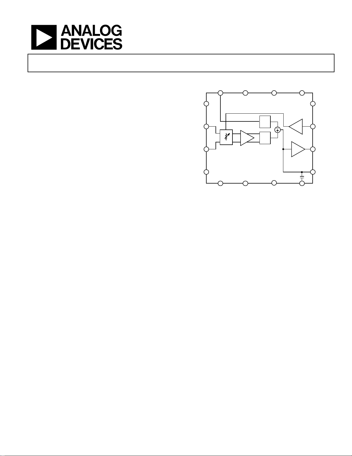
FUNCTIONAL BLOCK DIAGRAM
REF
11 10 9
2
CHPF
Figure 1. AD8363 Block Diagram
POS COMM
AD8363
2
X
2
X
3
VPOS
NC
INHI
TGT
12
13
14
15
16
1
TCM2/PWDN
AD8363
8
TEMP
VSET
7
6
VOUT
5
CLPF
4
COMM
07368-001
GENERAL DESCRIPTION
The AD8363 is a true rms responding power detector that
can be directly driven with a single-ended 50 Ω source. This
feature makes the AD8363 frequency versatile by eliminating
the need for a balun or any other form of external input tuning for
operation up to 6 GHz.
The AD8363 provides an accurate power measurement,
independent of waveform, for a variety of high frequency
communication and instrumentation systems. Requiring only
a single supply of 5 V and a few capacitors, it is easy to use and
provides high measurement accuracy. The AD8363 can operate
from arbitrarily low frequencies to 6 GHz and can accept inputs
that have rms values from less than −50 dBm to at least 0 dBm,
with large crest factors exceeding the requirements for accurate
measurement of WiMAX, CDMA, W-CDMA, TD-SCDMA,
multicarrier GSM, and LTE signals.
The AD8363 can determine the true power of a high frequency
signal having a complex low frequency modulation envelope, or
it can be used as a simple low frequency rms voltmeter. The highpass corner generated by its internal offset-nulling loop can be
lowered by a capacitor added on the CHPF pin.
Used as a power measurement device, VOUT is connected to
VSET. The output is then proportional to the logarithm of the
rms value of the input. The reading is presented directly in
decibels and is conveniently scaled to 52 mV/dB, or approximately
1 V per decade; however, other slopes are easily arranged. In
controller mode, the voltage applied to VSET determines the
power level required at the input to null the deviation from the
setpoint. The output buffer can provide high load currents.
The AD8363 has 1.5 mW power consumption when powered
down by a logic high applied to the TCM2/PWDN pin. It powers
up within about 30 µs to its nominal operating current of 60 mA at
25°C. The AD8363
is available in a 4 mm × 4 mm 16-lead LFCSP
for operation over the −40°C to +125°C temperature range.
A fully populated RoHS-compliant evaluation board is also
available.
Rev. A
Information furnished by Analog Devices is believed to be accurate and reliable. However, no
responsibility is assumed by Anal og Devices for its use, nor for any infringements of patents or ot her
rights of third parties that may result from its use. Specifications subject to change without notice. No
license is granted by implication or otherwise under any patent or patent rights of Analog Devices.
Trademarks and registered trademarks are the property of their respective owners.
One Technology Way, P.O. Box 9106, Norwood, MA 02062-9106, U.S.A.
Tel: 781.329.4700 www.analog.com
Fax: 781.461.3113 ©2009–2011 Analog Devices, Inc. All rights reserved.

AD8363
TABLE OF CONTENTS
Features.............................................................................................. 1
Applications....................................................................................... 1
Functional Block Diagram ..............................................................1
General Description......................................................................... 1
Revision History ...............................................................................2
Specifications..................................................................................... 3
Absolute Maximum Ratings............................................................ 7
ESD Caution.................................................................................. 7
Pin Configuration and Function Descriptions............................. 8
Typical Performance Characteristics............................................. 9
Theory of Operation ......................................................................14
Square Law Detector and Amplitude Target.............................. 14
RF Input Interface ......................................................................15
Choice of RF Input Pin.............................................................. 15
Small Signal Loop Response .....................................................15
Temperature Sensor Interface................................................... 16
VREF Interface ...........................................................................16
Temperature Compensation Interface..................................... 16
Power-Down Interface............................................................... 17
VSET Interface............................................................................ 17
Output Interface .........................................................................17
VTGT Interface .......................................................................... 18
Measurement Mode Basic Connections.................................. 18
System Calibration and Error Calculation.............................. 19
Operation to 125°C.................................................................... 19
Output Voltage Scaling.............................................................. 20
Offset Compensation, Minimum C
C
Capacitance Values............................................................ 20
HPF
Choosing a Value for C
RF Pulse Response and VTGT .................................................23
Controller Mode Basic Connections....................................... 23
Constant Output Power Operation.......................................... 24
Description of RF Characterization......................................... 25
Evaluation and Characterization Circuit Board Layouts...... 26
Assembly Drawings.................................................................... 28
Outline Dimensions....................................................................... 29
Ordering Guide .......................................................................... 29
.......................................................... 21
LPF
, and Maximum
LPF
REVISION HISTORY
7/11—Rev. 0 to Rev. A
Changes to Features Section and Applications Section............... 1
Added 3-Point Calibration to Table 1 for all MHz....................... 3
Replaced Typical Performance Characteristics Section;
Renumbered Sequentially................................................................ 9
Changes to Theory of Operation Section.................................... 14
Changes to Temperature Compensation Interface Section ...... 16
Changes to System Calibration and Error Calculation
Section and changes to Figure 44 and Figure 45........................ 19
Deleted Basis for Error Calculations Section and changes to
Figure 46 ..........................................................................................20
Deleted Selecting and Increasing Calibration Points to
Improve Accuracy over a Reduced Range Section..................... 22
Deleted Altering the Slope Section and added Output Voltage
Scaling Section ................................................................................23
5/09—Revision 0: Initial Version
Rev. A | Page 2 of 32

AD8363
SPECIFICATIONS
V
= 5 V, TA = 25°C, ZO = 50 Ω, single-ended input drive, VOUT connected to VSET, V
POS
referred to best-fit line (linear regression) from −20 dBm to −40 dBm, unless otherwise noted.
Table 1.
Parameter Conditions Min Typ Max Unit
OVERALL FUNCTION
Maximum Input Frequency 6 GHz
RF INPUT INTERFACE INHI (Pin 14), INLO (Pin 15), ac-coupled
Input Resistance Single-ended drive 50 Ω
Common-Mode DC Voltage 2.6 V
100 MHz TCM1 (Pin 16) = 0.47 V, TCM2 (Pin 1) = 1.0 V, INHI input
Output Voltage: High Power In PIN = −10 dBm 2.47 V
Output Voltage: Low Power In PIN = −40 dBm 0.92 V
±1.0 dB Dynamic Range CW input, TA = 25°C
3-point calibration at 0 dBm, −10 dBm, and −40 dBm 64 dB
Best-fit (linear regression) at −20 dBm and −40 dBm 65 dB
Maximum Input Level, ±1.0 dB 9 dBm
Minimum Input Level, ±1.0 dB −56 dBm
Deviation vs. Temperature Deviation from output at 25°C
−40°C < TA < +85°C; PIN = −10 dBm −0.2/+0.3 dB
−40°C < TA < +85°C; PIN = −40 dBm −0.5/+0.6 dB
Logarithmic Slope 51.7 mV/dB
Logarithmic Intercept −58 dBm
Deviation from CW Response 13 dB peak-to-rms ratio (W-CDMA), over 40 dB dynamic range <±0.1 dB
12 dB peak-to-rms ratio (WiMAX), over 40 dB dynamic range <±0.1 dB
256 QAM, CF = 8 dB, over 40 dB dynamic range <±0.1 dB
Input Impedance Single-ended drive 49 − j0.09 Ω
900 MHz TCM1 (Pin 16) = 0.5 V, TCM2 (Pin 1) = 1.2 V, INHI input
Output Voltage: High Power In PIN = −15 dBm 2.2 V
Output Voltage: Low Power In PIN = −40 dBm 0.91 V
±1.0 dB Dynamic Range CW input, TA = 25°C
3-point calibration at 0 dBm, −10 dBm, and −40 dBm 60 dB
Best-fit (linear regression) at −20 dBm and −40 dBm 54 dB
Maximum Input Level, ±1.0 dB −2 dBm
Minimum Input Level, ±1.0 dB −56 dBm
Deviation vs. Temperature Deviation from output at 25°C
−40°C < TA < +85°C; PIN = −15 dBm +0.6/−0.4 dB
−40°C < TA < +85°C; PIN = −40 dBm +0.8/−0.6 dB
Logarithmic Slope 51.8 mV/dB
Logarithmic Intercept −58 dBm
Deviation from CW Response 13 dB peak-to-rms ratio (W-CDMA), over 40 dB dynamic range <±0.1 dB
12 dB peak-to-rms ratio (WiMAX), over 40 dB dynamic range <±0.1 dB
256 QAM, CF = 8 dB, over 40 dB dynamic range <±0.1 dB
Input Impedance Single-ended drive 60 − j3.3 Ω
14.0 dB peak-to-rms ratio (16C CDMA2K), over 40 dB dynamic
range
14.0 dB peak-to-rms ratio (16C CDMA2K), over 40 dB dynamic
range
= 1.4 V, C
TGT
= 3.9 nF, C
LPF
<±0.1 dB
<±0.1 dB
= 2.7 nF, error
HPF
Rev. A | Page 3 of 32

AD8363
Parameter Conditions Min Typ Max Unit
1.9 GHz TCM1 (Pin 16) = 0.52 V, TCM2 (Pin 1) = 0.51 V, INHI input
Output Voltage: High Power In PIN = −15 dBm 2.10 V
Output Voltage: Low Power In PIN = −40 dBm 0.8 V
±1.0 dB Dynamic Range CW input, TA = 25°C
3-point calibration at 0 dBm, −10 dBm, and −40 dBm 56 dB
Best-fit (linear regression) at −20 dBm and −40 dBm 48 dB
Maximum Input Level, ±1.0 dB −6 dBm
Minimum Input Level, ±1.0 dB −53 dBm
Deviation vs. Temperature Deviation from output at 25°C
−40°C < TA < +85°C; PIN = −15 dBm +0.3/−0.5 dB
−40°C < TA < +85°C; PIN = −40 dBm +0.4/−0.4 dB
Logarithmic Slope 52 mV/dB
Logarithmic Intercept −55 dBm
Deviation from CW Response 13 dB peak-to-rms ratio (W-CDMA), over 37 dB dynamic range ±0.1 dB
12 dB peak-to-rms ratio (WiMAX), over 37 dB dynamic range ±0.1 dB
14.0 dB peak-to-rms ratio (16C CDMA2K), over 37 dB dynamic
range
256 QAM, CF = 8 dB, over 37 dB dynamic range ±0.1 dB
Input Impedance Single-ended drive 118 − j26 Ω
2.14 GHz TCM1 (Pin 16) = 0.52 V, TCM2 (Pin 1) = 0.6 V, INHI input
Output Voltage: High Power In PIN = −15 dBm 2.0 V
Output Voltage: Low Power In PIN = −40 dBm 0.71 V
±1.0 dB Dynamic Range CW input, TA = 25°C
3-point calibration at 0 dBm, −10 dBm and −40 dBm 55 dB
Best-fit (linear regression) at −20 dBm and −40 dBm 44 dB
Maximum Input Level, ±1.0 dB −8 dBm
Minimum Input Level, ±1.0 dB −52 dBm
Deviation vs. Temperature Deviation from output at 25°C
−40°C < TA < +85°C; PIN = −15 dBm +0.1/−0.2 dB
−40°C < TA < +85°C; PIN = −40 dBm +0.3/−0.5 dB
Logarithmic Slope 52.2 mV/dB
Logarithmic Intercept −54 dBm
Deviation from CW Response 13 dB peak-to-rms ratio (W-CDMA), over 35 dB dynamic range ±0.1 dB
12 dB peak-to-rms ratio (WiMAX), over 35 dB dynamic range ±0.1 dB
14.0 dB peak-to-rms ratio (16C CDMA2K), over 35 dB dynamic
range
256 QAM, CF = 8 dB, over 35 dB dynamic range ±0.1 dB
Rise Time
Fall Time
Transition from no input to 1 dB settling at RF
= 390 pF, C
C
LPF
= open
HPF
Transition from −10 dBm to within 1 dB of final value
(that is, no input level), C
= 390 pF, C
LPF
HPF
= −10 dBm,
IN
= open
Input Impedance Single-ended drive 130 − j49 Ω
2.6 GHz TCM1 (Pin 16) = 0.54 V, TCM2 (Pin 1) = 1.1 V, INHI input
Output Voltage: High Power In PIN = −15 dBm 1.84 V
Output Voltage: Low Power In PIN = −40 dBm 0.50 V
±1.0 dB Dynamic Range CW input, TA = 25°C
3-point calibration at 0 dBm, −10 dBm and −40 dBm 50 dB
Best-fit (linear regression) at −20 dBm and −40 dBm 41 dB
Maximum Input Level, ±1.0 dB −7 dBm
Minimum Input Level, ±1.0 dB −48 dBm
Deviation vs. Temperature Deviation from output at 25°C
−40°C < TA < +85°C; PIN = −15 dBm +0.5/−0.2 dB
−40°C < TA < +85°C; PIN = −40 dBm +0.6/−0.2 dB
±0.1 dB
±0.1 dB
3 µs
15 µs
Rev. A | Page 4 of 32

AD8363
Parameter Conditions Min Typ Max Unit
Logarithmic Slope 52.9 mV/dB
Logarithmic Intercept −49 dBm
Deviation from CW Response 13 dB peak-to-rms ratio (W-CDMA), over 32 dB dynamic range ±0.1 dB
12 dB peak-to-rms ratio (WiMAX), over 32 dB dynamic range ±0.1 dB
14.0 dB peak-to-rms ratio (16C CDMA2K), over 32 dB dynamic
range
256 QAM, CF = 8 dB, over 32 dB dynamic range ±0.1 dB
Input Impedance Single-ended drive 95 − j65 Ω
3.8 GHz TCM1 (Pin 16) = 0.56 V, TCM2 (Pin 1) = 1.0 V, INLO input
Output Voltage: High Power In PIN = −20 dBm 1.54 V
Output Voltage: Low Power In PIN = −40 dBm 0.54 V
±1.0 dB Dynamic Range CW input, TA = 25°C
3-point calibration at 0 dBm, −10 dBm and −40 dBm 50 dB
Best-fit (linear regression) at −20 dBm and −40 dBm 43 dB
Maximum Input Level, ±1.0 dB −5 dBm
Minimum Input Level, ±1.0 dB −48 dBm
Deviation vs. Temperature Deviation from output at 25°C
−40°C < TA < +85°C; PIN = −20 dBm +0.1/−0.7 dB
−40°C < TA < +85°C; PIN = −40 dBm +0.4/−0.5 dB
Logarithmic Slope 50.0 mV/dB
Logarithmic Intercept −51 dBm
Deviation from CW Response 13 dB peak-to-rms ratio (W-CDMA), over 32 dB dynamic range ±0.1 dB
12 dB peak-to-rms ratio (WiMAX), over 32 dB dynamic range ±0.1 dB
14.0 dB peak-to-rms ratio (16C CDMA2K), over 32 dB dynamic
range
256 QAM, CF = 8 dB, over 32 dB dynamic range ±0.1 dB
Input Impedance Single-ended drive 42 − j4.5 Ω
5.8 GHz TCM1 (Pin 16) = 0.88 V, TCM2 (Pin 1) = 1.0 V, INLO input
Output Voltage: High Power In PIN = −20 dBm 1.38 V
Output Voltage: Low Power In PIN = −40 dBm 0.36 V
±1.0 dB Dynamic Range CW input, TA = 25°C
3-point calibration at 0 dBm, −10 dBm and −40 dBm 50 dB
Best-fit (linear regression) at −20 dBm and −40 dBm 45 dB
Maximum Input Level, ±1.0 dB −3 dBm
Minimum Input Level, ±1.0 dB −48 dBm
Deviation vs. Temperature Deviation from output at 25°C
−40°C < TA < +85°C; PIN = −20 dBm +0.1/−0.6 dB
−40°C < TA < +85°C; PIN = −40 dBm +0.3/−0.8 dB
Logarithmic Slope 51.1 mV/dB
Logarithmic Intercept −47 dBm
Deviation from CW Response 13 dB peak-to-rms ratio (W-CDMA), over 32 dB dynamic range ±0.1 dB
12 dB peak-to-rms ratio (WiMAX), over 32 dB dynamic range ±0.1 dB
14.0 dB peak-to-rms ratio (16C CDMA2K), over 32 dB dynamic
range
256 QAM, CF = 8 dB, over 32 dB dynamic range ±0.1 dB
Input Impedance Single-ended drive 28 + j1.6 Ω
OUTPUT INTERFACE VOUT (Pin 6)
Output Swing, Controller Mode Swing range minimum, RL ≥ 500 Ω to ground 0.03 V
Swing range maximum, RL ≥ 500 Ω to ground 4.8 V
Current Source/Sink Capability Output held at V
Voltage Regulation I
Rise Time
= 8 mA, source/sink −0.2/+0.1 %
LOAD
Transition from no input to 1 dB settling at RF
= 390 pF, C
C
LPF
/2 10/10 mA
POS
= −10 dBm,
= open
HPF
IN
±0.1 dB
±0.1 dB
±0.1 dB
3 µs
Rev. A | Page 5 of 32

AD8363
Parameter Conditions Min Typ Max Unit
Fall Time
Transition from −10 dBm to within 1 dB of final value (that is,
no input level), C
= 390 pF, C
LPF
= open
HPF
Noise Spectral Density Measured at 100 kHz 45 nV/√Hz
SETPOINT INPUT VSET (Pin 7)
Voltage Range Log conformance error ≤ 1 dB, minimum 2.14 GHz 2.0 V
Log conformance error ≤ 1 dB, maximum 2.14 GHz 0.7 V
Input Resistance 72 kΩ
Logarithmic Scale Factor f = 2.14 GHz, −40°C ≤ TA ≤ +85°C 19.2 dB/V
Logarithmic Intercept f = 2.14 GHz, −40°C ≤ TA ≤ +85°C, referred to 50 Ω −54 dBm
TEMPERATURE COMPENSATION TCM1 (Pin 16), TCM2 (Pin 1)
Input Voltage Range 0 2.5 V
Input Bias Current, TCM1 V
V
Input Resistance, TCM1 V
Input Current, TCM2 V
V
V
V
Input Resistance, TCM2 0.7 V ≤ V
= 0 V −140 µA
TCM1
= 0.5 V 80 µA
TCM1
> 0.7 V 5 kΩ
TCM1
= 5 V 2 µA
TCM2
= 4.5 V 750 µA
TCM2
= 1 V −2 µA
TCM2
= 0 V −3 µA
TCM2
≤ 4.0 V 500 kΩ
TCM2
VOLTAGE REFERENCE VREF (Pin 11)
Output Voltage RFIN = −55 dBm 2.3 V
Temperature Sensitivity 25°C ≤ TA ≤ 70°C 0.04 mV/°C
70°C ≤ TA ≤ 125°C −0.06 mV/°C
−40°C ≤ TA ≤ +25°C −0.18 mV/°C
Current Source/Sink Capability 25°C ≤ TA ≤ 125°C 4/0.05 mA
−40°C ≤ TA < +25°C 3/0.05 mA
Voltage Regulation TA = 25°C, I
= 3 mA −0.6 %
LOAD
TEMPERATURE REFERENCE TEMP (Pin 8)
Output Voltage TA = 25°C, RL ≥ 10 kΩ 1.4 V
Temperature Coefficient −40°C ≤ TA ≤ +125°C, RL ≥ 10 kΩ 5 mV/°C
Current Source/Sink Capability 25°C ≤ TA ≤ 125°C 4/0.05 mA
−40°C ≤ TA < +25°C 3/0.05 mA
Voltage Regulation TA = 25°C, I
= 3 mA −0.1 %
LOAD
RMS TARGET INTERFACE VTGT (Pin 12)
Input Voltage Range 1.4 2.5 V
Input Bias Current V
= 1.4 V 14 µA
TGT
Input Resistance 100 kΩ
POWER-DOWN INTERFACE TCM2 (Pin1)
Logic Level to Enable VPWDN decreasing 4.2 V
Logic Level to Disable VPWDN increasing 4.7 V
Input Current V
V
V
V
Enable Time
Disable Time
= 5 V 2 µA
TCM2
= 4.5 V 750 µA
TCM2
= 1 V −2 µA
TCM2
= 0 V −3 µA
TCM2
TCM2 low to V
= 220 pF, RFIN = 0 dBm
C
HPF
TCM2 high to V
C
= 220 pF, RFIN = 0 dBm
HPF
at 1 dB of final value, C
OUT
OUT
at 1 dB of final value, C
= 470 pF,
LPF
= 470 pF,
LPF
POWER SUPPLY INTERFACE VPOS (Pin 3, Pin 10)
Supply Voltage 4.5 5 5.5 V
Quiescent Current TA = 25°C, RFIN = −55 dBm 60 mA
T
Power-Down Current V
= 85°C 72 mA
A
> V
TCM2
− 0.3 V 300 µA
POS
Rev. A | Page 6 of 32
15 µs
35 µs
25 µs
AD8363
ABSOLUTE MAXIMUM RATINGS
Table 2.
Parameter Rating
Supply Voltage, VPOS 5.5 V
Input Average RF Power1 21 dBm
Equivalent Voltage, Sine Wave Input 2.51 V rms
Internal Power Dissipation 450 mW
2
θ
10.6°C/W
JC
2
θ
35.3°C/W
JB
2
θ
57.2°C/W
JA
2
Ψ
1.0°C/W
JT
2
Ψ
34°C/W
JB
Stresses above those listed under Absolute Maximum Ratings
may cause permanent damage to the device. This is a stress
rating only; functional operation of the device at these or any
other conditions above those indicated in the operational
section of this specification is not implied. Exposure to absolute
maximum rating conditions for extended periods may affect
device reliability.
ESD CAUTION
Maximum Junction Temperature 150°C
Operating Temperature Range −40°C to +125°C
Storage Temperature Range −65°C to +150°C
Lead Temperature (Soldering, 60 sec) 300°C
1
This is for long durations. Excursions above this level, with durations much
less than 1 second, are possible without damage.
2
No airflow with the exposed pad soldered to a 4-layer JEDEC board.
Rev. A | Page 7 of 32

AD8363
T
PIN CONFIGURATION AND FUNCTION DESCRIPTIONS
NC
TCM1
INLO
INHI
14
13
16
15
PIN 1
INDICATOR
1TCM2/PWDN
2CHPF
AD8363
3VPOS
TOP VIEW
(Not to Scale)
4COMM
5
6
CLPF
NOTES
1. NC = NO CONNEC
Figure 2. Pin Configuration
VOUT
Table 3. Pin Function Descriptions
Pin No. Mnemonic Description
1 TCM2/PWDN
This is a dual function pin used for controlling the amount of nonlinear intercept temperature
compensation at voltages <2.5 V and/or for shutting down the device at voltages >4 V. If the
shutdown function is not used, this pin can be connected to the VREF pin through a voltage divider.
2 CHPF
Connect this pin to VPOS via a capacitor to determine the −3 dB point of the input signal high-pass filter.
Only add a capacitor when operating at frequencies below 10 MHz.
3, 10 VPOS
Supply for the Device. Connect these pins to a 5 V power supply. Pin 3 and Pin 10 are not
internally connected; therefore, both must connect to the source.
4, 9,
EPAD
COMM
System Common Connection. Connect these pins via low impedance to system common. The
exposed paddle is also COMM and should have both a good thermal and good electrical
connection to ground.
5 CLPF
Connection for Loop Filter Integration (Averaging) Capacitor. Connect a ground-referenced
capacitor to this pin. A resistor can be connected in series with this capacitor to improve loop
value is 390 pF.
LPF
6 VOUT
stability and response time. Minimum C
Output Pin in Measurement Mode (Error Amplifier Output). In measurement mode, this pin
is connected to VSET. This pin can be used to drive a gain control when the device is used in
controller mode.
7 VSET
The voltage applied to this pin sets the decibel value of the required RF input voltage that results
in zero current flow in the loop integrating capacitor pin, CLPF. This pin controls the variable gain
amplifier (VGA) gain such that a 50 mV change in VSET reduces the gain by approximately 1 dB.
8 TEMP Temperature Sensor Output. See Figure 35
11 VREF General-Purpose Reference Voltage Output of 2.3 V. See Figure 36
12 VTGT
The voltage applied to this pin determines the target power at the input of the RF squaring circuit.
The intercept voltage is proportional to the voltage applied to this pin. The use of a lower target
voltage increases the crest factor capacity; however, this may affect the system loop response.
13 NC No Connect. N/A
14 INHI
This is the RF input pin for frequencies up to and including 2.6 GHz. The RF input signal is
normally ac-coupled to this pin through a coupling capacitor.
15 INLO
This is the RF input pin for frequencies above 2.6 GHz. The RF input signal is normally ac-coupled
to this pin through a coupling capacitor.
16 TCM1
This pin is used to adjust the intercept temperature compensation. Connect this pin to VREF
through a voltage divider or to an external dc source.
12 VTGT
11 VREF
10 VPOS
9COMM
8
7
VSET
TEMP
07368-002
Equivalent
Circuit
See Figure 39
See Figure 48
N/A
N/A
See Figure 41
See Figure 41
See Figure 40
See Figure 42
See Figure 34
See Figure 34
See Figure 38
Rev. A | Page 8 of 32
AD8363
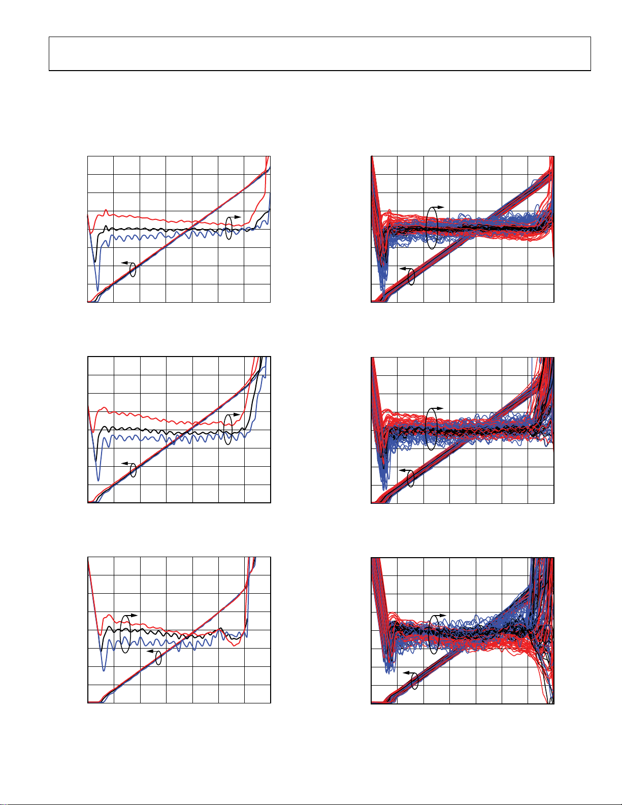
TYPICAL PERFORMANCE CHARACTERISTICS
V
= 5 V, ZO = 50 Ω, single-ended input drive, VOUT connected to VSET, V
POS
−40°C (blue), +85°C (red), where appropriate. Error calculated using 3-point calibration at 0 dBm, −10 dBm, and −40 dBm, unless
otherwise indicated. Input RF signal is a sine wave (CW), unless otherwise indicated.
4.0
4
= 1.4 V, C
TGT
4.0
= 3.9 nF, C
LPF
= 2.7 nF, TA = +25°C (black),
HPF
4
3.5
3.0
2.5
(V)
2.0
OUT
V
1.5
1.0
0.5
0
–60 –50 –40 –30 –20 –10 0 10
Figure 3. V
and Log Conformance vs. Input Power and
OUT
P
(dBm)
IN
3
2
1
0
–1
–2
–3
–4
Temperature at 100 MHz
4.0
3.5
3.0
2.5
(V)
2.0
OUT
V
1.5
1.0
0.5
0
–60 –50 –40 –30 –20 –10 0 10
Figure 4. V
and Log Conformance Error with Respect to 25°C Ideal Line
OUT
P
(dBm)
IN
4
3
2
1
0
–1
–2
–3
–4
over Temperature vs. Input Amplitude at 900 MHz, CW, Typical Device
4.0
4
3.5
3.0
2.5
(V)
2.0
OUT
ERROR (dB)
07368-103
V
1.5
1.0
0.5
0
–60 –50 –40 –30 –20 –10 0 10
Figure 6. Distribution of V
OUT
(dBm)
P
IN
and Error with Respect to 25°C Ideal Line over
3
2
1
0
ERROR (dB)
–1
–2
–3
–4
07368-106
Temperature vs. Input Amplitude at 100 MHz, CW
4.0
3.5
3.0
2.5
(V)
2.0
OUT
ERROR (dB)
07368-104
V
1.5
1.0
0.5
0
–60 –50 –40 –30 –20 –10 0 10
Figure 7. Distribution of V
P
(dBm)
IN
and Error with Respect to 25°C Ideal Line over
OUT
4
3
2
1
0
ERROR (dB)
–1
–2
–3
–4
07368-107
Temperature vs. Input Amplitude at 900 MHz, CW
4.0
4
3.5
3.0
2.5
(V)
2.0
OUT
V
1.5
1.0
0.5
0
–60 –50 –40 –30 –20 –10 0 10
Figure 5. V
and Log Conformance Error with Respect to 25°C Ideal Line
OUT
P
(dBm)
IN
3
2
1
0
–1
–2
–3
–4
over Temperature vs. Input Amplitude at 1.90 GHz, CW, Typical Device
ERROR (dB)
07368-105
Figure 8. Distribution of V
Rev. A | Page 9 of 32
3.5
3.0
2.5
(V)
2.0
OUT
V
1.5
1.0
0.5
0
–60 –50 –40 –30 –20 –10 0 10
OUT
(dBm)
P
IN
and Error with Respect to 25°C Ideal Line over
Temperature vs. Input Amplitude at 1.90 GHz, CW
3
2
1
0
ERROR (dB)
–1
–2
–3
–4
07368-108
AD8363
4.0
4
4.0
4
3.5
3.0
2.5
(V)
2.0
OUT
V
1.5
1.0
0.5
0
–60 –50 –40 –30 –20 –10 0 10
Figure 9. V
and Log Conformance Error with Respect to 25°C Ideal Line
OUT
P
(dBm)
IN
over Temperature vs. Input Amplitude at 2.14 GHz, CW, Typical Device
3.00
2.75
2.50
2.25
2.00
1.75
(V)
1.50
OUT
V
1.25
1.00
0.75
0.50
0.25
0
–60 –50 –40 –30 –20 –10 0 10
P
IN
(dBm)
3
2
1
0
ERROR (dB)
–1
–2
–3
–4
07368-109
3.5
3.0
2.5
(V)
2.0
OUT
V
1.5
1.0
0.5
0
–60 –50 –40 –30 –20 –10 0 10
Figure 12. Distribution of V
OUT
(dBm)
P
IN
and Error with Respect to 25°C Ideal Line over
3
2
1
0
ERROR (dB)
–1
–2
–3
–4
07368-112
Temperature vs. Input Amplitude at 2.14 GHz, CW
6
5
4
3
2
1
0
–1
ERROR (dB)
–2
–3
–4
–5
–6
07368-110
3.00
2.75
2.50
2.25
2.00
1.75
(V)
1.50
OUT
V
1.25
1.00
0.75
0.50
0.25
0
–60 –50 –40 –30 –20 –10 0 10
P
(dBm)
IN
6
5
4
3
2
1
0
–1
ERROR (dB)
–2
–3
–4
–5
–6
07368-113
Figure 10. V
and Log Conformance Error with Respect to 25°C Ideal Line
OUT
over Temperature vs. Input Amplitude at 2.6 GHz, CW, Typical Device
3.00
2.75
2.50
2.25
2.00
1.75
1.50
1.25
1.00
OUTPUT VOLTAGE (V)
0.75
0.50
0.25
0
–60 –50 –40 –30 –20 –10 0 10
Figure 11. V
and Log Conformance Error with Respect to 25°C Ideal Line
OUT
P
(dBm)
IN
over Temperature v s. Input Amplitude at 3.8 GHz, CW, Typical Device
6
5
4
3
2
1
0
–1
ERROR (dB)
–2
–3
–4
–5
–6
07368-111
Rev. A | Page 10 of 32
Figure 13. Distribution of V
and Error with Respect to 25°C Ideal Line over
OUT
Temperature vs. Input Amplitude at 2.6 GHz, CW
3.00
2.75
2.50
2.25
2.00
1.75
1.50
1.25
1.00
OUTPUT VOLTAGE (V)
0.75
0.50
0.25
0
–60 –50 –40 –30 –20 –10 0 10
Figure 14. Distribution of V
P
(dBm)
IN
and Error with Respect to 25°C Ideal Line over
OUT
Temperature vs. Input Amplitude at 3.8 GHz, CW
6
5
4
3
2
1
0
–1
ERROR (dB)
–2
–3
–4
–5
–6
07368-114

AD8363
3.00
2.75
2.50
2.25
2.00
1.75
1.50
1.25
1.00
OUTPUT VOLTAGE (V)
0.75
0.50
0.25
0
–60 –50 –40 –30 –20 –10 0 10
P
(dBm)
IN
6
5
4
3
2
1
0
–1
ERROR (dB)
–2
–3
–4
–5
–6
07368-115
3.00
2.75
2.50
2.25
2.00
1.75
1.50
1.25
1.00
OUTPUT VOLTAGE (V)
0.75
0.50
0.25
0
–60 –50 –40 –30 –20 –10 0 10
P
(dBm)
IN
6
5
4
3
2
1
0
–1
ERROR (dB)
–2
–3
–4
–5
–6
07368-118
Figure 15. V
and Log Conformance Error with Respect to 25°C Ideal Line
OUT
over Temperature vs. Input Amplitude at 5.8 GHz, Typical Device
3
2
1
0
ERROR (dB)
–1
–2
–3
–60 –50 –40 –30 –20 –10 0 10
ERROR CW
ERROR W-CDMA 1 CAR TM1 64 DPCH
ERROR W-CDMA 2 CAR TM1 64 DPCH
ERROR W-CDMA 3 CAR TM1 64 DPCH
ERROR W-CDMA 4 CAR TM1 64 DPCH
P
(dBm)
IN
Figure 16. Error from CW Linear Reference vs. Input Amplitude with
Modulation, Frequency at 2.14 GHz, C
= 0.1 μF, INHI Input
LPF
Figure 18. Distribution of V
and Error with Respect to 25°C Ideal Line
OUT
over Temperature vs. Input Amplitude at 5.8 GHz, CW
3
2
1
0
ERROR (dB)
–1
–2
–3
–60 –50 –40 –30 –20 –10 0 10
07368-026
CW
W-CDMA 1 CAR TM1 32 DPCH
QPSK
256QAM
WIMAX 256 SUBCR, 64 QAM, 10MHz BW
CDMA2K 9 CH SR1 4 CAR
P
(dBm)
IN
07368-028
Figure 19. Error from CW Linear Reference vs. Input Amplitude with
Modulation, Frequency at 2.6 GHz, C
160
140
120
= 0.1 μF, INHI Input
LPF
100MHz
900MHz
1.9GHz
5.8GHz
3.8GHz
2.14GHz
2.6GHz
Figure 17. Single-Ended Input Impedance (S11) vs.
Frequency; Z
= 50 Ω, INHI or INLO
O
07368-030
Rev. A | Page 11 of 32
100
80
60
40
NOISE SPECTRAL DENSIT Y (nV/ Hz)
20
0
100 1k 10k 100k 1M 10M
Figure 20. Typical Noise Spectral Density of V
FREQUENCY (Hz)
OUT
; All C
LPF
Values
07368-031

AD8363
(V)
OUT
V
5.0
0dBm –10dBm –20dBm –30dBm –40dBm
4.5
4.0
3.5
3.0
2.5
2.0
1.5
1.0
0.5
0
–0.5
–1.0
RF
ENVELOPE
TIME (µs)
12 13 14 15 16789101123456–2 –1 0 1
07368-033
(V)
OUT
V
5.0
0dBm –10dBm –20dBm –30dBm –40dBm
4.5
4.0
3.5
3.0
2.5
2.0
1.5
1.0
0.5
0
–0.5
–1.0
–2 2 4 6 8 10 12 14 16 18 20 22 24 26 28 300
RF
ENVELOPE
TIME (µs)
07368-035
Figure 21. Output Response to RF Burst Input, Carrier Frequency at 2.14 GHz,
= 390 pF, C
C
LPF
5.0
4.5
4.0
3.5
3.0
2.5
(V)
2.0
OUT
V
1.5
1.0
0.5
0
–0.5
–1.0
RF
ENVELOPE
= Open, Rising Edge
HPF
0dBm –10dBm –20d Bm
–30dBm –40dBm
234–1 0 1
TIME (ms)
5
07368-034
Figure 22. Output Response to RF Burst Input, Carrier Frequency at 2.14 GHz,
= 0.1 μF, C
C
LPF
6
5
(V)
OUT
OUTPUT VOLTAGE, V
TCM2 LOW TCM2 HIGH
4
3
2
1
0
0
255075
–50
–25
100
125
= Open, Rising Edge
HPF
150
175
200
225
250
TIME (µs)
275
300
325
350
375
0dBm
–50dBm
400
425
450
475
500
525
550
575
6
3
0
600
(V)
TCM2
V
07368-037
Figure 24. Output Response to RF Burst Input, Carrier Frequency at 2.14 GHz,
= 390 pF, C
C
LPF
5.0
4.5
4.0
3.5
3.0
2.5
(V)
2.0
OUT
V
1.5
1.0
0.5
0
–0.5
–1.0
= Open, Falling Edge
HPF
0dBm –10dBm –20d Bm
RF
ENVELOPE
TIME (ms)
–30dBm –40dBm
23–1 0 1
4
07368-036
Figure 25. Output Response to RF Burst Input, Carrier Frequency at 2.14 GHz,
= 0.1 μF, C
C
LPF
2.00
1.75
1.50
1.25
(V)
1.00
TEMP
V
0.75
0.50
0.25
0
–50–40–30 –20–10 0 10 20 30 40 50 60 70 80 90 100 110 120 130
= Open, Falling Edge
HPF
TEMPERATURE ( °C)
4
3
2
1
0
ERROR (°C)
–1
–2
–3
–4
07368-027
Figure 23. Output Response Using Power-Down Mode for Various RF Input
Levels Carrier Frequency at 2.14 GHz, C
= 470 pF, C
LPF
= 220 pF
HPF
Rev. A | Page 12 of 32
Figure 26. V
and Error with Respect to Straight Line vs. Temperature for
TEMP
Eleven Devices

AD8363
800
REPRESENTS
APPROXIMATELY
3000 PARTS FROM
SIX LOTS
REPRESENTS
600
APPROXIMATELY
3000 PARTS FROM
SIX LOTS
500
600
400
QUANTITY
200
0
1.34 1.36 1. 38 1.40 1. 42 1. 44 1. 46
Figure 27. Distribution of V
V
(V)
TEMP
Voltage at 25oC, No RF Input
TEMP
100
V
DECREASING
10
1
SUPPLY CURRENT (mA)
0.1
4.0 4.1 4. 2 4.3 4.4 4.5 4.6 4.7 4.8 4.9 5.0
TCM2
V
TCM2
(V)
V
TCM2
INCREASING
400
300
QUANTITY
200
100
0
2.24 2.26 2.28 2.30 2. 32 2. 34 2.36
07368-077
Figure 30. Distribution of V
(V)
V
REF
, 25°C, No RF Input
REF
07368-029
2.320
2.318
2.316
2.314
2.312
(V)
2.310
REF
V
2.308
2.306
2.304
2.302
2.300
4.5 4.6 4.7 4.8 4.9 5.0 5.1 5.2 5.3 5.4 5.5
07368-051
V
(V)
POS
07368-038
2.34
2.33
2.32
2.31
(V)
2.30
REF
V
2.29
2.28
2.27
2.26
–30 –25 – 20 –15 –10 –5 0 5 10
Figure 29. Change in V
Figure 28. Supply Current vs. V
P
(dBm)
IN
with Input Amplitude for Eleven Devices
REF
TCM2
07368-049
Rev. A | Page 13 of 32
Figure 31. Change in V
with V
REF
for Nine Devices
POS
2.325
2.320
2.315
2.310
(V)
REF
2.305
V
2.300
2.295
2.290
–40 –20 0 20 40 60 80 100 120
Figure 32. Change in V
TEMPERATURE (°C)
with Temperature for Eleven Devices
REF
07368-048

AD8363
V
THEORY OF OPERATION
The AD8363’s computational core is a high performance AGC
loop. As shown in Figure 33, the AGC loop comprises a wide
bandwidth variable gain amplifier (VGA), square law detectors, an
amplitude target circuit, and an output driver. For a more detailed
description of the functional blocks, see the AD8362 data sheet.
The nomenclature used in this data sheet to distinguish
between a pin name and the signal on that pin is as follows:
• The pin name is all uppercase (for example, VPOS,
COMM, and VOUT).
• The signal name or a value associated with that pin is the
pin mnemonic with a partial subscript (for example, C
C
HPF
, and V
OUT
).
LPF
,
SQUARE LAW DETECTOR AND AMPLITUDE TARGET
The VGA gain has the form
= GO exp(−V
G
SET
where:
G
is the basic fixed gain.
O
V
is a scaling voltage that defines the gain slope (the decibel
GNS
change per voltage). The gain decreases with increasing V
The VGA output is
V
= G
SIG
× RFIN = GO × RFIN exp(V
SET
where
RF
is the ac voltage applied to the input terminals of the AD8363.
IN
) (1)
SET/VGNS
.
SET
) (2)
SET/VGNS
The output of the VGA, V
, is applied to a wideband square
SIG
law detector. The detector provides the true rms response of the
RF input signal, independent of waveform. The detector output,
I
, is a fluctuating current with positive mean value. The
SQR
difference between I
I
, is integrated by CF and the external capacitor attached to
TGT
the CLPF pin at the summing node. C
capacitor, and C
and an internally generated current,
SQR
is an on-chip 25 pF filter
F
, the external capacitance connected to the
LPF
CLPF pin, can be used to arbitrarily increase the averaging time
while trading off with the response time. When the AGC loop is
at equilibrium
Mean(I
SQR
) = I
TGT
(3)
This equilibrium occurs only when
Mean(V
where V
2
) = V
SIG
is the voltage presented at the VTGT pin. This pin
TGT
2
(4)
TGT
can conveniently be connected to the VREF pin through a voltage
divider to establish a target rms voltage V
V
= 1.4 V.
TGT
of ~70 mV rms, when
ATG
Because the square law detectors are electrically identical and
well matched, process and temperature dependant variations
are effectively cancelled.
V
ATG
TGT
=
20
C
F
(INTERNAL)
AND BIAS
VTGT
CLPF
VOUT
COMM
TCM1
TCM2/PWDN
TEMP (1.4V)
VREF (2.3V)
07368-076
CHPF
INHI
INLO
VSET
C
H
(INTERNAL)
G
VPOS
C
(EXTERNAL)
SET
SUMMING
I
SQRITGT
2
X
NODE
HPF
VGA
V
SIG
Figure 33. Simplified Architecture Details
2
X
C
LPF
(EXTERNAL)
TEMPERATURE COMPENSATION
TEMPERATURE
SENSOR
BAND GAP
REFERENCE
Rev. A | Page 14 of 32

AD8363
V
By forcing the previous identity through varying the VGA setpoint,
it is apparent that
RMS(V
) = √(Mean(V
SIG
Substituting the value of V
RMS(G
× RFIN exp(−V
0
2
)) = √(V
SIG
from Equation 2 results in
SIG
SET/VGNS
When connected as a measurement device, V
for V
as a function of RFIN
OUT
V
OUT
= V
× log10(RMS(RFIN)/VZ) (7)
SLOPE
)) = V
ATG
2
ATG
) = V
SET
ATG
= V
. Solving
OUT
(5)
(6)
where:
V
is 1 V/decade (or 50 mV/dB).
SLOPE
is the intercept voltage.
V
Z
When RMS(RF
V
= 0 V, making the intercept the input that forces V
OUT
V
has been fixed to approximately 280 µV (approximately
Z
) = VZ, because log10(1) = 0, this implies that
IN
= 0 V.
OUT
−58 dBm, referred to 50 Ω) with a CW signal at 100 MHz.
In reality, the AD8363 does not respond to signals less than
~−56 dBm. This means that the intercept is an extrapolated
value outside the operating range of the device.
If desired, the effective value of V
can be altered by using
SLOPE
a resistor divider between VOUT and VSET. (Refer to the
Output Voltage Scaling section section for more information.)
In most applications, the AGC loop is closed through the
setpoint interface and the VSET pin. In measurement mode,
VOUT is directly connected to VSET. (See the Measurement
Mode Basic Connections section for more information.) In
controller mode, a control voltage is applied to VSET and the
VOUT pin typically drives the control input of an amplification
or attenuation system. In this case, the voltage at the VSET pin
forces a signal amplitude at the RF inputs of the AD8363 that
balances the system through feedback. (See the
Controller Mode Basic Connections section for more
information.)
RF INPUT INTERFACE
Figure 34 shows the connections of the RF inputs within the
AD8363. The input impedance is set primarily by an internal
50 Ω resistor connected between INHI and INLO. A dc level of
approximately half the supply voltage on each pin is established
internally. Either the INHI pin or the INLO pin can be used as
the single-ended RF input pin. (See the Choice of RF Input Pin
section.) If the dc levels at these pins are disturbed, performance is compromised; therefore, signal coupling capacitors must
be connected from the input signal to INHI and INLO. The
input signal high-pass corner formed by the coupling capacitors
and the internal resistances is
f
= 1/(2 × π × 50 × C) (8)
HIGH-PASS
where C is in farads and f
capacitors must be large enough in value to pass the input signal
frequency of interest. The other input pin should be RF accoupled to common (ground).
is in hertz. The input coupling
HIGH-PASS
VPOS
ESD
INHI
ESD
ESD ESD ESD ESD ESD ESD
ESD ESD ESD ESD ESD ESD
ESD
Figure 34. RF Inputs Simplified Schematic
BIAS
2.5kΩ 2.5kΩ
50Ω
ESD
ESD
INLO
07368-039
Extensive ESD protection is employed on the RF inputs, which
limits the maximum possible input amplitude to the AD8363.
CHOICE OF RF INPUT PIN
The dynamic range of the AD8363 can be optimized by choosing
the correct RF input pin for the intended frequency of operation.
Using INHI (Pin 14), users can obtain the best dynamic range at
frequencies up to 2.6 GHz. Above 2.6 GHz, it is recommended
that INLO (Pin 15) be used. At 2.6 GHz, the performance obtained
at the two inputs is approximately equal.
The AD8363 was designed with a single-ended RF drive in
mind. A balun can be used to drive INHI and INLO differentially, but it is not necessary, and it does not result in
improved dynamic range.
SMALL SIGNAL LOOP RESPONSE
The AD8363 uses a VGA in a loop to force a squared RF signal
to be equal to a squared dc voltage. This nonlinear loop can be
simplified and solved for a small signal loop response. The lowpass corner pole is given by
Freq
≈ 1.83 × I
LP
where:
I
is in amperes.
TGT
C
is in farads.
LPF
is in hertz.
Freq
LP
I
is derived from V
TGT
V
multiplied by a transresistance, namely
TGT
= gm × V
I
TGT
g
is approximately 18.9 µs, so with V
m
recommended 1.4 V, I
this current varies with temperature; therefore, the small signal
pole varies with temperature. However, because the RF squaring
circuit and dc squaring circuit track with temperature, there is no
temperature variation contribution to the absolute value of V
For CW signals,
Freq
≈ 67.7 × 10⁻⁶/(C
LP
However, signals with large crest factors include low
pseudorandom frequency content that either needs to be
filtered out or sampled and averaged out. See the Choosing a
Valu e fo r CL PF section for more information.
/(C
) (9)
LPF
; however, I
TGT
is approximately 37 µA. The value of
TGT
) (11)
LPF
is a squared value of
TGT
equal to the typically
TGT
TGT
TGT
2
OUT
(10)
.
Rev. A | Page 15 of 32

AD8363
V
V
TEMPERATURE SENSOR INTERFACE
The AD8363 provides a temperature sensor output with an
output voltage scaling factor of approximately 5 mV/°C. The
output is capable of sourcing 4 mA and sinking 50 µA maximum at
temperatures at or above 25°C. If additional current sink capability
is desired, an external resistor can be connected between the
TEMP and COMM pins. The typical output voltage at 25°C is
approximately 1.4 V.
POS
INTERNAL
VPAT
TEMP
12kΩ
4kΩ
COMM
Figure 35. TEMP Interface Simplified Schematic
07368-041
VREF INTERFACE
The VREF pin provides an internally generated voltage reference.
The V
capable of sourcing 4 mA and sinking 50 µA maximum at
temperatures at or above 25°C. An external resistor can be
connected between the VREF and COMM pins to provide
additional current sink capability. The voltage on this pin can be
used to drive the TCM1, TCM2/PWDN, and VTGT pins, if desired.
voltage is a temperature stable 2.3 V reference that is
REF
POS
INTERNAL
VO LTAG E
VREF
The values in Table 4 were chosen to give the best drift
performance at the high end of the usable dynamic range
over the −40°C to +85°C temperature range.
Compensating the device for the temperature drift using TCM1
and TCM2/PWDN allows for great flexibility and the user may
wish to modify these values to optimize for another amplitude
point in the dynamic range, for a different temperature range,
or for an operating frequency other than those shown in Tabl e 4.
To find a new compensation point, V
swept while monitoring V
over the temperature at the
OUT
TCM1
and V
TCM2
can be
frequency and amplitude of interest. The optimal voltages for
V
and V
TCM1
power and frequency are the values of V
has minimum movement. See the AD8364 and ADL5513
V
OUT
to achieve minimum temperature drift at a given
TCM2
and V
TCM1
TCM2
where
data sheets for more information.
Var yin g V
TCM1
and V
has only a very slight effect on V
TCM2
OUT
at
device temperatures near 25°C; however, the compensation circuit
has more and more effect, and is more and more necessary for
best temperature drift performance, as the temperature departs
farther from 25°C.
Figure 37 shows the effect on temperature drift performance at
25°C and 85°C as V
3
2
1
0
is varied but V
TCM1
V
TCM1
= 0.62V
is held constant at 0.6 V.
TCM2
16kΩ
COMM
07368-042
Figure 36. VREF Interface Simplified Schematic
TEMPERATURE COMPENSATION INTERFACE
Proprietary techniques are used to maximize the temperature
stability of the AD8363. For optimal performance, the output
temperature drift must be compensated for using the TCM1 and
TCM2/PWDN pins. The absolute value of compensation varies
with frequency and V
for the TCM1 and TCM2/PWDN pins to maintain the best
temperature drift error over the rated temperature range (−40°C <
T
< 85°C) when driven single-ended and using a V
A
Table 4. Recommended Voltages for TCM1 and TCM2/PWDN
Frequency TCM1 (V) TCM2/PWDN (V)
100 MHz 0.47 1.0
900 MHz 0.5 1.2
1.9 GHz 0.52 0.51
2.14 GHz 0.52 0.6
2.6 GHz 0.54 1.1
3.8 GHz 0.56 1.0
5.8 GHz 0.88 1.0
. Table 4 shows the recommended voltages
TGT
= 1.4 V.
TGT
ERROR (dB)
–1
–2
–3
–60 –50 –40 –30 –20 –10 0 10
Figure 37. Error vs. Input Amplitude over Stepped V
o
25
V
= 0.42V
TCM1
RF
(dBm)
IN
C and 85oC, 2.14 GHz, V
TCM2
25°C
85°C
= 0.6 V
TCM1
Values,
07368-050
TCM1 primarily adjusts the intercept of the AD8363 at
temperature. In this way, TCM1 can be thought of as a coarse
adjustment to the compensation. Conversely, TCM2 performs a
fine adjustment. For this reason, it is advised that when searching
for compensation with V
first, and when best performance is found, V
TCM1
and V
TCM2
, that V
be adjusted
TCM1
can then be
TCM2
adjusted for optimization.
It is evident from Figure 37 that the temperature compensation
circuit can be used to adjust for the lowest drift at any input
amplitude of choice. Though not shown in Figure 37, a similar
analysis can simultaneously be performed at −40°C, or any
other temperature within the operating range of the AD8363.
Performance varies slightly from device to device; therefore,
optimal V
TCM1
and V
values must be arrived at statistically
TCM2
Rev. A | Page 16 of 32

AD8363
V
V
V
over a population of devices to be useful in mass production
applications.
The TCM1 and TCM2 pins have high input impedances,
approximately 5 kΩ and 500 kΩ, respectively, and can be
conveniently driven from an external source or from a fraction
of V
by using a resistor divider. V
REF
does change slightly with
REF
temperature and RF input amplitude (see Figure 32 and Figure 29);
however, the amount of change is unlikely to result in a significant
effect on the final temperature stability of the RF measurement system.
Figure 38 shows a simplified schematic representation of TCM1.
See the Power-Down Interface section for the TCM2 interface.
POS
3kΩ
ESD
3kΩ
ESD
COMM
ESD
TCM1
07368-043
Figure 38. TCM1 Interface Simplified Schematic
POWER-DOWN INTERFACE
The quiescent and disabled currents for the AD8363 at 25°C are
approximately 60 mA and 300 µA, respectively. The dual function
pin, TCM2/PWDN, is connected to a temperature compensation
circuit as well as a power-down circuit. Typically, when PWDN
is greater than V
Figure 28 shows this characteristic as a function of V
that because of the design of this section of the AD8363, as
V
passes through a narrow range at ~4.5 V (or ~V
TCM2
the TCM2/PWDN pin sinks approximately 750 µA. The source
used to disable the AD8363 must have a sufficiently high current
capability for this reason. Figure 23 shows the typical response
times for various RF input levels. The output reaches within 0.1
dB of its steady-state value in approximately 35 µs; however, the
reference voltage is available to full accuracy in a much shorter
time. This wake-up response varies depending on the input
coupling and the capacitances, C
POS
− 0.1 V, the device is fully powered down.
POS
PWDN
− 0.5 V),
POS
HPF
and C
LPF
.
. Note
VSET INTERFACE
The VSET interface has a high input impedance of 72 kΩ.
The voltage at VSET is converted to an internal current used
to set the internal VGA gain. The VGA attenuation control is
approximately 19 dB/V.
GAIN ADJUST
54kΩ
VSET
18kΩ
2.5kΩ
COMM
Figure 40. VSET Interface Simplified Schematic
07368-045
OUTPUT INTERFACE
The output driver used in the AD8363 is different from the
output stage on the AD8362. The AD8363 incorporates rail-torail output drivers with pull-up and pull-down capabilities. The
closed-loop −3 dB bandwidth of the VOUT buffer with no load
is approximately 58 MHz with a single-pole roll-off of −20 dB/dec.
The output noise is approximately 45 nV/√Hz at 100 kHz, which
is independent of C
VOUT can source and sink up to 10 mA. There is an internal
load between VOUT and COMM of 2.5 kΩ.
CLPF
ESD
Figure 41. VOUT Interface Simplified Schematic
due to the architecture of the AD8363.
LPF
POS
ESD
2pF
ESD
COMM
2kΩ
500Ω
VOUT
07368-046
ESD
TCM2/
PWDN
COMM
SHUTDOW N
CIRCUIT
200Ω
ESD
POWER-UP
CIRCUIT
7kΩ 7kΩ
200Ω
200Ω
INTERCEPT
TEMPERATURE
COMPENS ATION
VREF
ESD
07368-044
Figure 39. PWDN Interface Simplified Schematic
Rev. A | Page 17 of 32

AD8363
V
V
VTGT INTERFACE MEASUREMENT MODE BASIC CONNECTIONS
The target voltage can be set with an external source or by
connecting the VREF pin (nominally 2.3 V) to the VTGT pin
through a resistive voltage divider. With 1.4 V on the VTGT pin,
the rms voltage that must be provided by the VGA to balance the
AGC feedback loop is 1.4 V × 0.05 = 70 mV rms. Most of the
characterization information in this data sheet was collected at
V
= 1.4 V. Voltages higher and lower than this can be used;
TGT
however, doing so increases or decreases the gain at the internal
squaring cell, which results in a corresponding increase or
decrease in intercept. This in turn affects the sensitivity and the
usable measurement range. Because the gain of the squaring
cell varies with temperature, oscillations or a loss in measurement
range can result. For these reasons, do not reduce V
POS
ESD
VTGT
ESD
COMM
Figure 42. VTGT Interface Simplified Schematic
50kΩ
50kΩ
ESD
10kΩ
below 1.3 V.
TGT
2
g × X
ITGT
07368-047
The AD8363 requires a single supply of nominally 5 V. The
supply is connected to the two supply pins, VPOS. Decouple
the pins using two capacitors with values equal or similar to
those shown in Figure 43. These capacitors must provide a low
impedance over the full frequency range of the input, and they
should be placed as close as possible to the VPOS pins. Use two
different capacitor values in parallel to provide a broadband ac
short to ground.
Input signals can be applied differentially or single-ended; however,
in both cases, the input impedance is 50 Ω. Most performance
information in this data sheet was derived with a single-ended
drive. The optimal measurement range is achieved using a singleended drive on the INHI pin at frequencies below 2.6 GHz (as
shown in Figure 43), and likewise, optimal performance is achieved
using the INLO pin above 2.6 GHz (similar to Figure 43; except
INLO is ac-coupled to the input and INHI is ac-coupled to ground).
The AD8363 is placed in measurement mode by connecting
VOUT to VSET. This closes the AGC loop within the device
with V
representing the VGA control voltage, which is
OUT
required to present the correct rms voltage at the input of the
internal square law detector.
POS2
C7
VREF
0.1µF
LOW FRE QUENCY INPUT
C10
0.1µF
C12
0.1µF
TCM1
R11
1.4kΩ
13
14
15
16
NC
INHI
INLO
TCM1
TCM2/PWDN
R10
845Ω
12 11 10 9
VTGT
VREF
VPOS
AD8363
DUT1
TCM2/PWDN
CHPF
VPOS
1234
C3
OPEN
100pF
VPOS1
Figure 43. Measurement Mode Basic Connections
C5
TEMP
COMM
8
TEMP
7
VSET
6
VOUT
5
CLPF
COMM
C4
100pF
C13
0.1µF
PADDLE
AGND
C9
0.1µF
VOUT
7368-062
Rev. A | Page 18 of 32

AD8363
SYSTEM CALIBRATION AND ERROR CALCULATION
The measured transfer function of the AD8363 at 1.9 GHz is
shown in Figure 44, which contains plots of both output voltage
vs. input amplitude (power) and calculated error vs. input level. As
the input level varies from −55 dBm to +0 dBm, the output
voltage varies from ~0 V to ~3.1 V.
Because slope and intercept vary from device to device, boardlevel calibration must be performed to achieve high accuracy.
The equation for the idealized output voltage can be written as
V
OUT(IDEAL)
where:
Slope is the change in output voltage divided by the change in
input power (dB).
4.0
3.5
3.0
2.5
(V)
2.0
OUT
V
1.5
1.0
0.5
Figure 44. 1.9 GHz Transfer Function and Linearity Error using a Two-Point
Intercept is the calculated input power level at which the output
voltage would equal 0 V (note that Intercept is an extrapolated
theoretical value not a measured value).
In general, calibration, which establishes the Slope and Intercept,
is performed during equipment manufacture by applying two
or more known signal levels to the input of the AD8363 and
measuring the corresponding output voltages. The calibration
points are generally chosen within the linear-in-dB operating
range of the device.
With a two-point calibration, the slope and intercept are
calculated as follows:
Slope = (V
Intercept = P
After the slope and intercept are calculated and stored in nonvolatile memory during equipment calibration, an equation can
be used to calculate an unknown input power based on the
output voltage of the detector.
P
IN
The log conformance error is the difference between this
straight line and the actual performance of the detector.
Error (dB) = (V
= Slope × (PIN − Intercept) (12)
4
3
2
1
0
ERROR (dB)
–1
–2
–3
0
–60 –50 –40 –30 –20 –10 0 10
P
(dBm)
IN
Calibration (Calibration Points −20 dBm and −40 dBm)
− V
)/(P
− P
OUT1
− (V
IN1
(Unknown) = (V
OUT(MEASURED)
OUT2
IN1
/Slope) (14)
OUT1
OUT1(MEASURED)
) (13)
IN2
/Slope) + Intercept (15)
− V
)/Slope (16)
OUT(IDEAL)
–4
07368-144
Rev. A | Page 19 of 32
Figure 44 includes a plot of this error when using a two-point
calibration (calibration points are −20 dBm and −40 dBm). The
error at the calibration points is equal to 0 by definition.
The residual nonlinearity of the transfer function that is
apparent in the two-point calibration error plot can be reduced
by increasing the number of calibration points. Figure 45 shows
the post-calibration error plots for three-point calibration. With
a multipoint calibration, the transfer function is segmented,
with each segment having its own slope and intercept. During
calibration, multiple known power levels are applied, and
multiple voltages are measured. When the equipment is in
operation, the measured voltage from the detector is first used
to determine which of the stored slope and intercept calibration
coefficients are to be used. Then the unknown power level is
calculated by inserting the appropriate slope and intercept into
Equation 15.
Figure 45 shows the output voltage and error at 25°C and over
temperature when a three-point calibration is used (calibration
points are 0 dBm, −10 dBm and −40 dBm). When choosing
calibration points, there is no requirement for, or value in
equal spacing between the points. There is also no limit to the
number of calibration points used.
4.0
3.5
3.0
2.5
(V)
2.0
OUT
V
1.5
1.0
0.5
0
–60 –50 –40 –30 –20 –10 0 10
P
(dBm)
IN
Figure 45. 1.9 GHz Transfer Function and Error at +25°C, −40°C, and +85°C
Using a Three-Point Calibration (0 dBm, −10 dBm and −40 dBm)
4
3
2
1
0
ERROR (dB)
–1
–2
–3
–4
07368-145
The −40°C and +85°C error plots in Figure 45 and Figure 45
are generated using the 25°C calibration coefficients. This is
consistent with equipment calibration in a mass production
environment where calibration at just a single temperature is
practical.
OPERATION TO 125°C
The AD8363 operates up to 125°C with slightly degraded
performance. Figure 46 shows the typical operation (Errors are
plotted using two-point calibration) at 125°C as compared to other
temperatures using the TCM1 and TCM2 values in Table 4.
Temperature compensation can be optimized for operation
above 85°C by modifying the voltages on the TCM1 and TCM2
pins from those shown in Tabl e 4 .

AD8363
Figure 46. V
6
5
4
3
2
OUTPUT VOLTAGE (V)
1
0
–60 –50 –40 –30 –20 –10 0 10
and Log Conformance Error vs. Input Amplitude at 2.14 GHz,
OUT
–40°C
+25°C
+85°C
+125°C
INHI INPUT
V
TCM1
P
(dBm)
IN
−40°C to +125°C
= 0.52V, V
TCM2
= 0.6V
3
2
1
0
ERROR (d B)
–1
–2
–3
07368-053
OUTPUT VOLTAGE SCALING
The output voltage range of the AD8363 (nominally 0 V to
3.5 V) can be easily increased or decreased. There are a number
of situations where adjustment of the output scaling makes
sense. For example, if the AD8363 is driving an analog-todigital converter (ADC) with a 0 V to 5 V input range, it makes
sense to increase the detector’s nominal maximum output
voltage of 3.5 V so that it is closer to 5 V. This makes better use
of the input range of the ADC and maximizes the resolution of
the system in terms of bits/dB.
If only a part of the AD8363’s RF input power range is being
used (for example, −10 dBm to −40 dBm), it may make sense to
increase the scaling so that this reduced input range fits into the
AD8363’s available output swing of 0 V to 4.8 V.
The output swing can be reduced by adding a voltage divider on
the output pin, as shown in Figure 47 (with VOUT connected
directly to VSET and a resistor divider on VOUT). Figure 47
also shows how the output voltage swing can be increased using
a technique that is analogous to setting the gain of an op amp in
noninverting mode. With the VSET pin being the equivalent of
the inverting input of the op amp, a resistor divider is connected
between VOUT and VSET.
R2
VSET
7
R1
VOUT
6
R2
Figure 47. Decreasing and Increasing Slope
Equation 17 is the general function that governs this.
'
⎞
⎛
V
O
(17)
⎟
⎜
RR2R1
−= 1)||(
IN
⎟
⎜
V
O
⎠
⎝
7
6
VSET
VOUT
R1
07368-146
Rev. A | Page 20 of 32
where:
V
is the nominal maximum output voltage (see Figure 4
O
through Figure 18).
V'
is the new maximum output voltage (for example, up
O
to 4.8 V).
R
is the VSET input resistance (72 kΩ).
IN
When choosing R1 and R2, attention must be paid to the
current drive capability of the VOUT pin and the input
resistance of the VSET pin. The choice of resistors should not
result in excessive current draw out of VOUT. However, making
R1 and R2 too large is also problematic. If the value of R2 is
compatible with the 72 kΩ input resistance of the VSET input,
this input resistance, which varies slightly from part to part,
contributes to the resulting slope and output voltage. In general,
the value of R2 should be at least ten times smaller than the
input resistance of VSET. Values for R1 and R2 should, therefore,
be in the 1 k to 5 k range.
It is also important to take into account part-to-part and
frequency variation in output swing along with the AD8363
output stage’s maximum output voltage of 4.8 V. The V
OUT
distribution is well characterized at major frequencies’ bands
in the Typical Performance Characteristics section (Figure 3 to
Figure 18).
OFFSET COMPENSATION, MINIMUM C
MAXIMUM C
CAPACITANCE VALUES
HPF
LPF
, AND
An offset-compensation loop is used to eliminate small dc
offsets within the internal VGA as shown in Figure 48. The
high-pass corner frequency of this loop is set to about 1 MHz
using an on-chip 25 pF capacitor. Because input signals that are
below 1 MHz will be interpreted to be unwanted offset voltages,
this restricts the operating frequency range of the device. To
operate the AD8363 at lower frequencies (than 1 MHz), the highpass corner frequency must be reduced by connecting a
capacitor between CHPF and VPOS.
Internal offset voltages vary depending on the gain at which the
VGA is operating and, therefore, on the input signal amplitude.
When a large C
value is used, the offset correction process can
HPF
lag the more rapid changes in the gain of the VGA, which can
increase the time required for the loop to fully settle for a given
steady input amplitude. This can manifest itself in a jumpy,
seemingly oscillatory response of the AD8363.
Care should therefore be taken in choosing C
HPF
and C
LPF
because there is a potential to create oscillations. In general, make
the capacitance on the CLPF pin as large as possible; there is no
maximum on the amount of capacitance that can be added to
this pin. At high frequencies, there is no need for an external
capacitor on the CHPF pin; therefore, the pin can be left open.
However, when trying to get a fast response time and/or when
working at low frequencies, extra care in choosing the proper
capacitance values for C
control pin (VSET) connected to VOUT, V
determined by the on-chip squaring cell and C
HPF
and C
is prudent. With the gain
LPF
can slew at a rate
SET
. When V
LPF
SET
is
changing with time, the dc offsets in the VGA also vary with

AD8363
V
time. The speed at which V
that falls within the high-pass corner set by C
measurement mode, take care to set C
slews can create a time varying offset
SET
. Therefore, in
HPF
appropriately to reduce
LPF
the slew. It is also worth noting that most of the typical
performance data was derived with C
= 3.9 nF and C
LPF
= 2.7 nF
HPF
and with a CW waveform.
The minimum appropriate C
based on slew rate limitations is
LPF
as follows
C
> 20 × 10−3/FREQ
LPF
RFIN
(18)
where:
C
is in farads.
LPF
FREQ
This takes into account the on-chip 25 pF capacitor, C
parallel with C
is in hertz.
RFIN
. However, because there are other internal
LPF
, in
F
device time delays that affect loop stability, use a minimum
C
of 390 pF.
LPF
The minimum appropriate C
for a given high-pass pole
HPF
frequency is
C
= 29.2 × 10⁻⁶/FHP
HPF
where FHP
is in hertz.
POLE
− 25 pF (19)
POLE
The subtraction of 25 pF is a result of the on-chip 25 pF
capacitor in parallel with the external C
C
to give a pole (3 dB corner) at least 1 decade below the
HPF
. Typically, choose
HPF
desired signal frequency. Note that the high pass corner of the
offset compensation system is approximately 1 MHz without an
external C
; therefore, adding an external capacitor lowers the
HPF
corner frequency.
The following example illustrates the proper selection of the input
coupling capacitors, minimum C
, and maximum C
LPF
HPF
when
using the AD8363 in measurement mode for a 1 GHz input signal.
1. Choose the input coupling capacitors that have a 3 dB
corner at least one decade below the input signal frequency.
From Equation 8, C > 10/(2 × π × RF
× 50) = 32 pF
IN
minimum. According to this calculation, 32 pF is sufficient;
however, the input coupling capacitors should be a much
larger value, typically 0.1 µF. The offset compensation
circuit, which is connected to CHPF, should be the true
determinant of the system high-pass corner frequency and
not the input coupling capactitors. With 0.1 µF coupling
capacitors, signals as low as 32 kHz can couple to the input,
which will be well below the system high-pass frequency.
2. Choose C
See Equation 18, where FRQ
C
> 20 pF. However, as previously mentioned, values below
LPF
to reduce instabilities due to V
LPF
= 1 GHz, and this results in
RFIN
slew rate.
SET
390 pF are not recommended. For this reason, a 470 pF
capacitor was chosen. In addition, if fast response times are
not required, an even larger C
value than given here
LPF
should be chosen.
3. Choose C
system. See Equation 19, where FHP
to set a 3 dB corner to the offset compensation
HPF
is in this case
POLE
100 MHz, one decade below the desired signal. This results
in a negative number and, obviously, a negative value is not
practical. Because the high-pass corner frequency is already
1 MHz, this result simply illustrates that the appropriate
solution is to use no external C
capacitor.
HPF
Note that per Equation 9
≈ 1.83 × I
Freq
LP
A C
of 470 pF results in a small signal low-pass corner
LPF
TGT
/(C
LPF
)
frequency of approximately 144 kHz. This reflects the bandwidth
of the measurement system, and how fast the user can expect
changes on the output. It does not imply any limitations on the
input RF carrier frequency.
POS
110Ω 110Ω
VGA
gm
RFIN
A = 1
Figure 48. Offset Compensation Circuit
CHOOSING A VALUE FOR C
25pF
(INTERNAL)
gm2
40dB
1pF 1pF
CHPF
gm1
V
X
2
g × X
IRF
LPF
The Small Signal Loop Response section and the Offset
Compensation, Minimum CLPF, and Maximum CHPF
Capacitance Values section discussed how to choose the
minimum value capacitance for C
based on a minimum
LPF
capacitance of 390 pF, slew rate limitation, and frequency of
operation. Using the minimum value for C
allows the quickest
LPF
response time for pulsed type waveforms (such as WiMAX) but
also allows the most residual ripple on the output caused by the
pseudorandom modulation waveform. There is not a maximum
for the capacitance that can be applied to the CLPF pin, and in
most situations, a large enough capacitor can be added to remove
the residual ripple caused by the modulation and yet allow a fast
enough response to changes in input power.
Figure 49 shows how residual ripple, rise time, and fall time
vary with filter capacitance when the AD8363 is driven by a
single carrier CDMA2000 9CH SR1 signal at 2.14 GHz. The rise
time and fall time is based on a signal that is pulsed between no
signal and 10 dBm but is faster if the input power change is less.
07368-040
Rev. A | Page 21 of 32

AD8363
400
350
300
250
200
RESIDUAL RIPP LE (mV)
RISE TIM E (µs)
FAL L T IM E ( µ s)
2800
2450
2100
1750
1400
Figure 50 shows how the rise time cuts off the preamble. Note
that the power in the preamble can be easily measured; however,
the C
value would have to be reduced slightly, and the noise in
LPF
the main signal would increase.
T
150
RISE TIME (µs)
100
RESIDUAL RIP PLE (mV p -p)
50
0
0 102030405060708090100
CAPACITANCE (nF)
C
LPF
Figure 49. Residual Ripple, Rise Time, and Fall Time vs. C
LPF
1050
700
350
0
Capacitance,
FALL TIME (µs)
07368-069
Single Carrier CDMA2000 9CH SR1 Signal at 2.14 GHz with 10 dBm Pulse
Table 5 shows the recommended values of C
modulation schemes. For nonpulsed waveforms, increase C
for popular
LPF
LPF
until
the residual output noise falls below 50 mV (±0.5 dB). In each case,
the capacitor can be increased to further reduce the noise. A 10%
to 90% step response to an input step is also listed. Where the
increased response time is unacceptably high, reduce C
, which
LPF
increases the noise on the output. Due to the random nature of the
output ripple, if it is sampled by an ADC, averaging in the digital
domain further reduces the residual noise.
Table 5 gives C
values to minimize noise while trying to keep
LPF
a reasonable response time. For non-pulsed type waveforms,
averaging is not required on the output. For pulsed waveforms,
the smaller the noise, the less averaging is needed on the output.
System specifications determine the necessary rise time and fall
time. For example, the suggested C
value for WiMAX assumes
LPF
that it is not necessary to measure the power in the preamble.
CH1 RISE
81.78µs
CH1 FALL
1.337ms
1
CH1 500mV M 1.00ms A CH1 600mV
T 10.00%
07368-054
Figure 50. AD8363 Output Response to a WiMAX 802.16, 64 QAM, 256
Subcarriers, 10 MHz Bandwidth Signal with C
= 0.027 μF
LPF
As shown in Figure 49, the fall time for the AD8363 increases
faster than the rise time with an increase in C
capacitance.
LPF
Some pulse-type modulation standards require a fast fall time as
well as a fast rise time, and in all cases, less output ripple is desired.
Placing an RC filter on the output reduces the ripple, according
to the frequency content of the ripple and the filter’s poles and
zeros. Using an RC output filter also changes the rise and fall
time vs. the output ripple response as compared to increasing
the C
capacitance.
LPF
Table 5. Recommended C
Modulation/Standard Crest Factor (dB) C
Values for Various Modulation Schemes
LPF
LPF
Residual Ripple
(mV p-p)
Response Time (Rise/Fall)
10% to 90%
W-CDMA, 1Carrier, TM1-64 12 0.1 µF 15 236 s/2.9 ms
W-CDMA, 1Carrier, TM1-64 (EVDO) 12 3900 pF 150 8.5 s/100 µs
W-CDMA, 4Carrier, TM1-64 11 0.1 µF 8 240 s/2.99 ms
CDMA2000, 1Carrier, 9CH 9.1 0.1 µF 10 210 s/3.1 ms
CDMA2000, 3Carrier, 9CH 11 0.1 µF 13 215 s/3.14 ms
WiMAX 802.16 , 64 QAM, 256 Subcarriers, 10 MHz Bandwidth 14 0.027 µF 10 83 µs/1.35 ms
6C TD-SCDMA 14 0.01 µF 69 24 s/207 s
1C TD-SCDMA 11.4 0.01 µF 75 24 s /198 s
Rev. A | Page 22 of 32

AD8363
Figure 51 shows the response for a 2.14 GHz pulsed signal,
with C
= 3900 pF. The residual ripple from a single carrier
LPF
CDMA2000 9CH SR1 signal is 150 mV p-p. (The ripple is not
shown in Figure 51. The ripple was measured separately.) Figure 52
shows the response for a 2.14 GHz pulse signal with a C
LPF
of
390 pF and an output filter that consists of a series 75 resistor
(closest to the output) followed by a 0.15 µF capacitor to ground.
The residual ripple for this configuration is also 150 mV p-p.
Note that the rise time is faster and the fall time is slower when
the larger C
1
CH1 500mV M 100µs A CH1 720mV
Figure 51. Pulse Response with C
Ripple for a Single Carrier CDMA2000 9CH SR1 Signal at 2.14 GHz
is used to obtain a 150 mV p-p ripple.
LPF
T
T 10.40%
= 3900 pF Resulting in a 150 mV p-p
LPF
T
8
TEMP
VSET
7
75Ω
VOUT
6
CLPF
5
390pF
OSCILLOSCOPE
PROBE
0.15µF
CH1 RISE
8.480µs
CH1 FALL
101.4µs
CH1 AMPL
2.37V
CH1 RISE
13.66µs
CH1 FALL
35.32µs
07368-070
CONTROLLER MODE BASIC CONNECTIONS
In addition to being a measurement device, the AD8363 can
also be configured to control rms signal levels, as shown in
Figure 53.
The RF input to the device is configured as it was in measurement
mode and either input can be used. A directional coupler taps
off some of the power being generated by the VGA. If loss in
the main signal path is not a concern, and there are no issues
with reflected energy from the next stage in the signal chain, a
power splitter can be used instead of a directional coupler. Some
additional attenuation may be required to set the maximum
input signal at the AD8363 to be equal to the recommended
maximum input level for optimum linearity and temperature
stability at the frequency of operation.
The VSET and VOUT pins are no longer shorted together. VOUT
now provides a bias or gain control voltage to the VGA. The gain
control sense of the VGA must be negative and monotonic, that is,
increasing voltage tends to decrease gain. However, the gain
control transfer function of the device does not need to be well
controlled or particularly linear. If the gain control sense of the
VGA is positive, an inverting op amp circuit with a dc offset
shift can be used between the AD8363 and the VGA to keep the
gain control voltage in the 0.03 V to 4.8 V range.
VSET becomes the set-point input to the system. This can be
driven by a DAC, as shown in Figure 53, if the output power is
expected to vary, or it can simply be driven by a stable reference
voltage, if constant output power is required. This DAC should
have an output swing that covers the 0.15 V to 3.5 V range. The
AD7391 and AD7393 serial input and parallel input 10-bit DACs
provide adequate resolution (4 mV/bit) and an adjustable
output swing over 4.5 V.
CH1 AMPL
1
CH1 500mV M 100µs A CH1 750mV
Figure 52. Pulse Response with C
T 10.60%
= 390 pF and Series 75 Ω Resistor
LPF
2.36V
07368-071
Followed by a 0.15 μF Capacitor to Ground, Resulting in a 150 mV p-p
Ripple for a Single Carrier CDMA2000 9CH SR1 Signal at 2.14 GHz
RF PULSE RESPONSE AND VTGT
The response of the AD8363 to pulsed RF waveforms is affected
by V
. Referring to Figure 21 and Figure 22, there is a period
TGT
of inactivity between the start of the RF waveform and the time
at which V
the implementation of the balancing of the squarer currents within
the AD8363. This delay can be reduced by decreasing V
however, as previously noted in the VTGT Interface section,
this has implications on the sensitivity, intercept, and dynamic
range. While the delay is reduced, reducing V
rise and fall time of V
begins to show a reaction. This happens as a result of
OUT
TGT
increases the
TGT
.
OUT
;
Rev. A | Page 23 of 32
VGA OR VVA
(OUTPUT POWER
P
IN
DECREASES AS
V
INCREASES)
APC
V
APC
(0.03V TO 4.8V AVAIL ABLE SWING)
VOUT
INHI
C10
P
OUT
ATTENUAT OR
AD8363
INLO
C12
C9
SEE TEXT
DAC
CLPF
VSET
(0.15V TO 3.5V)
Figure 53. Controller Mode Operation for Automatic Power Control
When V
is set to a particular value, the AD8363 compares this
SET
value to the equivalent input power present at the RF input. If
these two values do not match, V
increases or decreases in
OUT
an effort to balance the system. The dominant pole of the error
amplifier/integrator circuit that drives V
is set by the capacitance
OUT
07368-063

AD8363
–
on the CLPF pin; some experimentation may be necessary to
choose the right value for this capacitor.
In general, C
should be chosen to provide stable loop operation
LPF
for the complete output power control range. If the slope (in
dB/V) of the gain control transfer function of the VGA is not
constant, C
the gain control slope is at its maximum. In addition, C
must be chosen to guarantee a stable loop when
LPF
LPF
must
provide adequate averaging to the internal low range squaring
detector so that the rms computation is valid. Larger values of C
LPF
tend to make the loop less responsive.
The relationship between V
and the RF input follows the
SET
measurement mode behavior of the device. For example, Figure 4
shows the measurement mode transfer function at 900 MHz
and that an input power of −10 dBm yields an output voltage
of approximately 2.5 V. Therefore, in controller mode, if V
SET
is
2.5 V, the AD8363 output would go to whatever voltage is
necessary to set the AD8363 input power to −10 dBm.
CONSTANT OUTPUT POWER OPERATION
In controller mode, the AD8363 can be used to hold the output
power of a VGA stable over a broad temperature/input power
range. This is useful in topologies where a transmit card is driving
an HPA, or when connecting any two power sensitive modules
together.
Figure 54 shows a schematic of a circuit setup that holds the output
power to approximately −26 dBm at 2.14 GHz, when the input
power is varied over a 40 dB dynamic range. Figure 55 shows
the results. A portion of the output power is coupled off using
a 10 dB directional coupler, and it is then fed into the AD8363.
V
is fixed at 0.95 V, which forces to AD8363 output voltage
SET
to control the ADL5330 so that the input to the AD8363 is
approximately −36 dBm.
If the AD8363 was in measurement mode and a −36 dBm input
power is applied, the output voltage would be 0.95 V. A generalpurpose, rail-to-rail op amp (AD8062) is used to invert the slope
of the AD8363 so that the gain of the ADL5330 decreases as
the AD8363 control voltage increases. The output power is
controlled to a 10 dB higher power level than that seen by the
AD8363 due to the coupler. The high-end power is limited by
the linearity of the VGA (ADL5330) with high attenuation and
can be increased by using a higher linearity VGA.
The low end power is limited by the maximum gain of the VGA
(ADL5330) and can be increased by using a VGA with more
gain. The temperature performance is directly related to the
temperature performance of the AD8363 at 2.14 GHz and
−26 dBm, using TCM1 = 0.52 V and TCM2 = 0.6 V. All other
temperature variations are removed by the AD8363.
10dB
C5
P
IN
100pF
T1 T2
C6
100pF
0.52V I NHITCM1
INHI
INLO
10kΩ
10kΩ 10kΩ
ADL5330
OPHI
OPLO
GAIN
AD8062
10kΩ
5V
VOUT
C11
100pF
C12
100pF
C10
0.1µF
COUPLER
P
OUT
AD8363
0.6V
TCM2
VSET
0.95V
INLO
CLPF
C9
0.1µF
C12
0.1µF
Figure 54. Constant Power Circuit
25.0
–25.5
–26.0
–26.5
(dBm)
OUT
P
–27.0
–27.5
–28.0
–40 –35 –30 –25 –20 –15 –10 –5 0
P
(dBm)
IN
–20°C
–40°C
+85°C
+25°C
0°C
07368-055
Figure 55. Performance of the Circuit Shown in Figure 54
07368-072
Rev. A | Page 24 of 32

AD8363
DESCRIPTION OF RF CHARACTERIZATION
The general hardware configuration used for most of the AD8363
characterization is shown in Figure 56. The AD8363 was driven
in a single-ended configuration for all characterization.
Characterization of the AD8363 employed a multisite test
strategy. Several AD8363 devices mounted on circuit boards
constructed with Rogers 3006 material was simultaneously
inserted into a remotely-controlled thermal test chamber.
A Keithley S46 RF switching network connected an Agilent
E8251A signal source to the appropriate device under test. An
Agilent 34980A switch matrix provided switching of dc power
and metering for the test sites. A PC running Agilent VEE Pro
controlled the signal source, switching, and chamber temperature.
A voltmeter measured the subsequent response to the stimulus,
and the results were stored in a database for later analysis. In this
way, multiple AD8363 devices were characterized over amplitude,
frequency, and temperature in a minimum amount of time.
The RF stimulus amplitude was calibrated up to the connector
of the circuit board that carries the AD8363. However, the
calibration does not account for the slight losses due to the
connector and the traces from the connector to the device
under test. For this reason, there is a small absolute amplitude
error (<0.5 dB) not accounted for in the characterization data.
This implies a slight error in the reported intercept; however,
this is generally not important because the slope and the relative
accuracy of the AD8363 are not affected.
The typical performance data was derived with C
and C
= 2.7 nF with a CW waveform.
HPF
= 3.9 nF
LPF
AGILENT E3631A
DC POWER
SUPPLIES
AGILENT E8251A
MICROWAVE
SIGNAL
GENERATOR
RF DC DATA AND CONTROL
PERSONAL
COMPUTER
Figure 56. General RF Characterization Configuration
AGILENT 34980A
SWITCH MATRIX/
DC METER
KEITHLEY S46
MICROWAVE
SWITCH
AD8363
CHARACTERIZ ATION
BOARD – TEST SI TE 1
AD8363
CHARACTERIZ ATION
BOARD – TEST SI TE 2
AD8363
CHARACTERIZ ATION
BOARD – TEST SI TE 3
07368-075
Rev. A | Page 25 of 32

AD8363
V
V
V
POS
C7
0.1µF
EVALUATION AND CHARACTERIZATION CIRCUIT BOARD LAYOUTS
Figure 57 to Figure 61 show the evaluation board for the AD8363.
TGT
REF
VPOS
VPOS
C3
OPEN
R14
0Ω
R16
4
0Ω
VPOS
C5
100pF
COMM
COMM
VPOS1
TEMP
VSET
VOUT
CLPF
C4
100pF
C13
0.1µF
TEMP
8
7
6
5
PADDLE
AGND
R2
OPEN
R6
0Ω
R5
0Ω
C9
0.1µF
GND
R13
OPEN
VSET
R1
0Ω
C8
OPEN
VOUT
GNDI
R15
0Ω
VOUT
07368-074
R7
0Ω
R11
1.4kΩ
R18
OPEN
VREFC
TCM2/PWDN
R12
OPEN
13
14
15
16
OPEN
NC
INHI
INLO
TCM1
R9
VREFC
C10
C11
0.1µF
C6
OPEN
OPEN
C12
0.1µF
TCM1
R17
OPEN
IN
R10
845Ω
12 11 10 9
123
VPOSC
R8
0Ω
VTGT
VREF
AD8363
DUT1
TCM2/PWDN
CHPF
Figure 57. Evaluation Board Schematic
Rev. A | Page 26 of 32

AD8363
Table 6. Evaluation Board Configuration Options
Component Function/Notes Default Value
C6, C10,
C11, C12
R7, R8,
R10, R11
C4, C5, C7,
C13, R14, R16
R1, R2, R6,
R13, R15
C8, C9, R5
C3
R9, R12
R17, R18
Paddle Connect the paddle to both a thermal and electrical ground.
Input. The AD8363 is single-ended driven. At frequencies ≤2.6 GHz, the best dynamic range is achieved by
driving Pin 14 (INHI). When driving INHI, populate C10 and C12 with an appropriate capacitor value for
the frequency of operation and leave C6 and C11 open. For frequencies >2.6 GHz, additional dynamic
range can be achieved by driving Pin 15 (INLO). When driving INLO, populate C6 and C11 with an appropriate
capacitor value for the frequency of operation and leave C10 and C12 open.
VTGT. R10 and R11 are set up to provide 1.4 V to VTGT from VREF. If R10 and R11 are removed, an external
voltage can be used. Alternatively, R7 and R11 can be used to form a voltage divider for an external reference.
Power Supply Decoupling. The nominal supply decoupling consists of a 100 pF filter capacitor placed
physically close to the AD8363, a 0 Ω series resistor, and a 0.1 µF capacitor placed close to the power
supply input pin. The 0 Ω resistor can be replaced with a larger resistor to add more filtering; however,
it is at the expense of a voltage drop.
Output Interface (Default Configuration) in Measurement Mode. In this mode, a portion of the output
voltage is fed back to the VSET pin via R6. Using the voltage divider created by R2 and R6, the magnitude
of the slope at VOUT is increased by reducing the portion of VOUT that is fed back to VSET. If a fast
responding output is expected, the 0 Ω resistor (R15) can be removed to reduce parasitics on
the output.
Output Interface in Controller Mode. In this mode, R6 must be open and R13 must have a 0 Ω resistor.
In controller mode, the AD8363 can control the gain of an external component. A setpoint voltage is
applied to the VSET pin, the value of which corresponds to the desired RF input signal level applied to
the AD8363. If a fast responding output is expected, the 0 Ω resistor (R15) can be removed to reduce
parasitics on the output.
Low-Pass Filter Capacitors, C
pulse response time of the AD8363. This capacitor should be as large as possible. The smallest C
. The low-pass filter capacitors reduce the noise on the output and affect the
LPF
LPF
capacitance should be 390 pF. R5, when set to a value other than 0 Ω, is used in conjunction with C8 and
C9 to modify the loop transfer function and change the loop dynamics in controller mode.
Capacitor. The C
C
HPF
and can also affect the response time. The C
capacitor introduces a high-pass filter affect into the AD8363 transfer function
HPF
capacitor should be as small as possible and connect to
HPF
VPOS when used. No capacitor is needed for input frequencies greater than 10 MHz.
TCM2/PWDN. The TCM2/PWDN pin controls the amount of nonlinear intercept temperature compensation
and/or shuts down the device. The evaluation board is configured to control this from a test loop, but VREF
can also be used by the voltage divider created by R9 and R12.
TCM1. TCM1 controls the temperature compensation (5 kΩ impedance). The evaluation board is configured to
control this from a test loop, but VREF can also be used by the voltage divider created by R17 and R18.
Due to the relatively low impedance of the TCM1 pin and the limited current of the VREF pin, care should
be taken when choosing the R17 and R18 values.
C6 = open,
C10 = 0.1 µF,
C11 = open
C12 = 0.1 µF
R7 = 0 Ω,
R8 = 0 Ω,
R10 = 845 Ω,
R11 = 1.4 kΩ
C4 = 100 pF,
C5 = 100 pF,
C7 = 0.1µF,
C13 = 0.1µF,
R14 = 0 Ω,
R16 = 0 Ω
R1 = 0 Ω,
R2 = open,
R6 = 0 Ω,
R13 = open,
R15 = 0 Ω
C8 = open,
C9 = 0.1 µF,
R5 = 0 Ω
C3 = open
R9 = open,
R12 = open
R17 = open,
R18 = open
Rev. A | Page 27 of 32

AD8363
ASSEMBLY DRAWINGS
07368-060
07368-061
Figure 58. Evaluation Board Layout, Top Side
Figure 59. Evaluation Board Layout, Bottom Side
07368-058
Figure 60. Evaluation Board Assembly, Top Side
7368-059
Figure 61. Evaluation Board Assembly, Bottom Side
Rev. A | Page 28 of 32

AD8363
OUTLINE DIMENSIONS
4.00
PIN 1
INDICATOR
1.00
0.85
0.80
12° MAX
SEATING
PLANE
BSC SQ
TOP
VIEW
0.80 MAX
0.65 TYP
COMPLIANT TO JEDEC STANDARDS MO-220-VG GC
0.35
0.30
0.25
3.75
BSC SQ
0.20 REF
0.60 MAX
0.65 BSC
0.05 MAX
0.02 NOM
COPLANARIT Y
0.50
0.40
0.30
0.08
Figure 62. 16-Lead Lead Frame Chip Scale Package [LFCSP_VQ]
4 mm × 4mm Body, Very Thin Quad
(CP-16-10)
Dimensions shown in millimeters
ORDERING GUIDE
1
Model
AD8363ACPZ-R2 −40°C to +125°C 16-Lead Lead Frame Chip Scale Package [LFCSP_VQ] CP-16-10 250
AD8363ACPZ-R7 −40°C to +125°C 16-Lead Lead Frame Chip Scale Package [LFCSP_VQ] CP-16-10 1,500
AD8363ACPZ-WP −40°C to +125°C 16-Lead Lead Frame Chip Scale Package [LFCSP_VQ] CP-16-10 64
AD8363-EVALZ Evaluation Board
1
Z = RoHS Compliant Part.
Temperature Range Package Description Package Option Ordering Quantity
0.60 MAX
13
16
12
EXPOSED
(BOTTOM VIEW)
9
8
1.95 BSC
1
PA D
4
5
FOR PROPER CONNECTION O F
THE EXPOSED PAD, REFER TO
THE PIN CONF IGURATION AND
FUNCTION DES CRIPTIO NS
SECTION O F THIS DAT A SHEET.
PIN 1
INDICATOR
2.50
2.35 SQ
2.20
0.25 MIN
082008-A
Rev. A | Page 29 of 32

AD8363
NOTES
Rev. A | Page 30 of 32

AD8363
NOTES
Rev. A | Page 31 of 32

AD8363
NOTES
©2009–2011 Analog Devices, Inc. All rights reserved. Trademarks and
registered trademarks are the property of their respective owners.
D07368-0-7/11(A)
Rev. A | Page 32 of 32
 Loading...