

50 Hz to 2.7 GHz
V
VTGT
FEATURES
Complete fully calibrated measurement/control system
Accurate rms-to-dc conversion from 50 Hz to 2.7 GHz
Input dynamic range of >60 dB: −52 dBm to +8 dBm in 50 Ω
Waveform and modulation independent:
(Such as GSM/CDMA/TDMA)
Linear-in-decibels output, scaled 50 mV/dB
Law conformance error of 0.5 dB
All functions temperature and supply stable
Operates from 4.5 V to 5.5 V at 24 mA from −40°C to +85°C
Power-down capability to 1.3 mW
APPLICATIONS
Power amplifier linearization/control loops
Transmitter power control
Transmitter signal strength indication (TSSI)
RF instrumentation
GENERAL DESCRIPTION
The AD8362 is a true rms-responding power detector that has a
60 dB measurement range. It is intended for use in a variety of
high frequency communication systems and in instrumentation
requiring an accurate response to signal power. It is easy to use,
requiring only a single supply of 5 V and a few capacitors. It can
operate from arbitrarily low frequencies to over 2.7 GHz and
can accept inputs that have rms values from 1 mV to at least
1 V rms, with peak crest factors of up to 6, exceeding the
requirements for accurate measurement of CDMA signals.
The input signal is applied to a resistive ladder attenuator
that comprises the input stage of a variable gain amplifier.
The 12 tap points are smoothly interpolated using a proprietary
technique to provide a continuously variable attenuator, which
is controlled by a voltage applied to the VSET pin. The resulting
signal is applied to a high performance broadband amplifier. Its
output is measured by an accurate square-law detector cell. The
fluctuating output is then filtered and compared with the output
of an identical squarer, whose input is a fixed dc voltage applied
to the VTGT pin, usually the accurate reference of 1.25 V
provided at the VREF pin.
The difference in the outputs of these squaring cells is
integrated in a high gain error amplifier, generating a voltage at
the VOUT pin with rail-to-rail capabilities. In a controller
mode, this low noise output can be used to vary the gain of a
host system’s RF amplifier, thus balancing the set point against
Rev. B
Information furnished by Analog Devices is believed to be accurate and reliable.
However, no responsibility is assumed by Analog Devices for its use, nor for any
infringements of patents or other rights of third parties that may result from its use.
Specifications subject to change without notice. No license is granted by implication
or otherwise under any patent or patent rights of Analog Devices. Trademarks and
registered trademarks are the property of their respective owners.
60 dB TruPwr™ Detector
AD8362
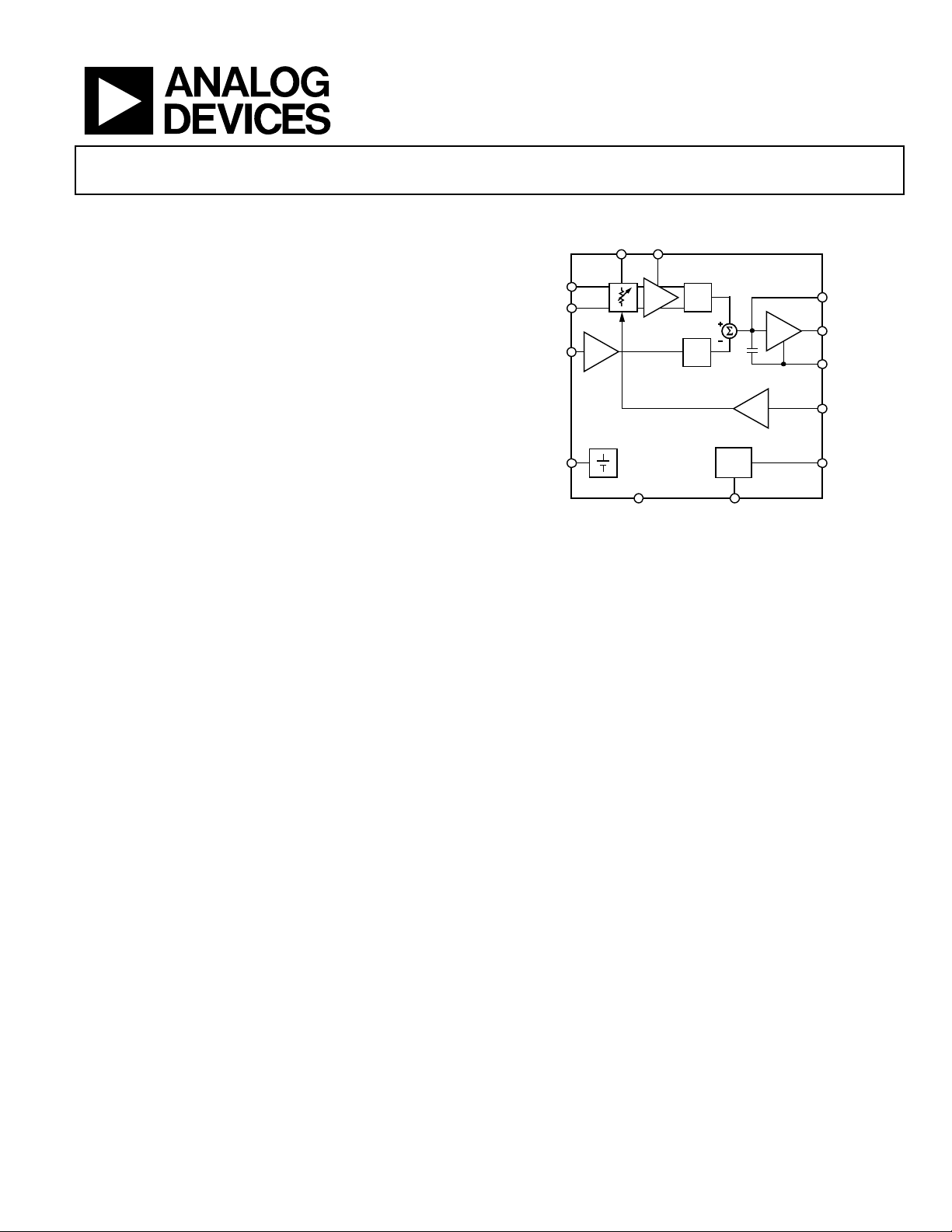
FUNCTIONAL BLOCK DIAGRAM
CHPF
DECL
INHI
INLO
AD8362
REF
the input power. Optionally, the voltage at VSET may be a
replica of the RF signal’s amplitude modulation, in which case
the overall effect is to remove the modulation component prior
to detection and low-pass filtering. The corner frequency of the
averaging filter may be lowered without limit by adding an
external capacitor at the CLPF pin. The AD8362 can be used to
determine the true power of a high frequency signal having a
complex low frequency modulation envelope (or simply as a
low frequency rms voltmeter). The high-pass corner generated
by its offset-nulling loop can be lowered by a capacitor added
on the CHPF pin.
Used as a power measurement device, VOUT is strapped to
VSET, and the output is then proportional to the logarithm of
the rms value of the input; that is, the reading is presented
directly in decibels and is conveniently scaled 1 V per decade,
that is, 50 mV/dB; other slopes are easily arranged. In controller
modes, the voltage applied to VSET determines the power level
required at the input to null the deviation from the setpoint.
The output buffer can provide high load currents.
The AD8362 is powered down by a logic high applied to the
PWDN pin, i.e., the consumption is reduced to about 1.3 mW. It
powers up within about 20 µs to its nominal operating current
of 20 mA at 25°C. The AD8362 is supplied in a 16-lead TSSOP
package for operation over the industrial temperature range of
−40°C to +85°C. An evaluation board is available.
One Technology Way, P.O. Box 9106, Norwood, MA 02062-9106, U.S.A.
Tel: 781.329.4700 www.analog.com
Fax: 781.326.8703 © 2004 Analog Devices, Inc. All rights reserved.
2
x
2
x
Figure 1.
BIAS
PWDNCOMM
CLPF
VOUT
ACOM
VSET
VPOS
02923-B-001

AD8362
TABLE OF CONTENTS
Specifications ...................................................................................3
Uncertainties in R
and Power Calibration............................ 24
IN
Absolute Maximum Ratings ..........................................................6
ESD Caution.................................................................................. 6
Pin Configuration and Function Description .............................7
Equivalent Circuits..........................................................................8
Typical Performance Characteristics............................................ 9
Characterization Setup .................................................................14
Equipment................................................................................... 14
Analysis........................................................................................ 14
Circuit Description........................................................................15
Square-Law Detection ...............................................................15
Effect of Input Coupling on the Intercept Value.................... 16
Offset Elimination...................................................................... 16
Voltage vs. Power Calibration ................................................... 17
Effect of Signal Waveform......................................................... 17
Operation at Low Frequencies.................................................. 17
Choosing the Right Value for CHPF and CLPF..................... 24
Use of Nonstandard Target Voltages........................................ 24
Adjusting the Intercept ..............................................................25
Altering the Slope....................................................................... 25
Envelope Elimination Mode..................................................... 26
Operator in Controller Modes ....................................................27
Use of an Input Balun................................................................ 27
General Applications ....................................................................29
RMS Voltmeter with >100 dB Dynamic Range...................... 29
RF Power Meter with 80 dB Range.......................................... 30
High Slope Detectors Centered on a Narrow Window......... 31
AD8362 Evaluation Board........................................................ 32
Outline Dimensions...................................................................... 34
Ordering Guide .......................................................................... 34
REVISION HISTORY
Time-Domain Response of the Closed Loop .........................17
Alteration of the Internal Target Voltage................................. 18
Effects at Each End of Dynamic Range................................... 18
Input Protection.......................................................................... 19
Power-Enable Response Time .................................................. 19
Using the AD8362......................................................................... 20
Basic Connections...................................................................... 20
Main Modes of Operation............................................................ 21
Operation in Measurement Modes.............................................22
Law Conformance Error............................................................ 22
Alternative Input Coupling Means ..........................................23
Using a Narrow-Band Input Match .........................................23
3/04—Data Sheet Changed from Rev. A to Rev. B.
Updated Format.................................................................Universal
Changes to Specifications............................................................... 3
Changes to the Offset Elimination Section................................16
Changes to the Operation at Low Frequencies Section............17
Changes to the Time-Domain Response of the Closed Loop
Section............................................................................................. 17
Changes to Equation 13................................................................ 24
Changes to Table 5......................................................................... 31
6/03—Data Sheet Changed from Rev. 0 to Rev. A.
Updated Ordering Guide................................................................ 5
Change to Analysis Section.......................................................... 12
Updated AD8362 Evaluation Board Section .............................26
2/03—Revision 0: Initial Version
Rev. B | Page 2 of 36

AD8362
SPECIFICATIONS
VS = 5 V, T = 25°C, ZO = 50 Ω, differential input drive via Balun1, VTGT connec ted to VREF, VOUT tied to VSET, unl ess other wise note d.
Table 1.
Parameter Conditions Min Typ Max Unit
OVERALL FUNCTION
Maximum Input Frequency 2.7 GHz
Input Power Range (Differential)
Nominal Low End of Range −52 dBm
Nominal High End of Range +8 dBm
Input Voltage Range (Differential)
Nominal Low End of Range 1.12 mV rms
Nominal High End of Range 1.12 V rms
Input Power Range (S-Sided)
Nominal Low End of Range −40 dBm
Nominal High End of Range 0 dBm
Input Voltage Range (S-Sided) RMS Voltage at Input Terminals, f ≤ 2.7 GHz
Nominal Low End of Range 2.23 mV rms
Nominal High End of Range 223 V rms
Output Voltage Range RL ≥ 200 Ω to Ground
Nominal Low End of Range +100 mV
Nominal High End of Range In General, VS – 0.1 V +4.9 V
Output Scaling (Log Slope) 50 mV/dB
Law Conformance Error Over Central 60 dB Range, f ≤ 2.7 GHz ±0.5 dB
RF INPUT INTERFACE Pins INHI, INLO, AC-Coupled
Input Resistance Single-Ended Drive, wrt DECL 100 Ω
Differential Drive 200 Ω
OUTPUT INTERFACE Pin VOUT
Available Output Range RL ≥ 200 Ω to Ground 0.1 4.9 V
Absolute Voltage Range
Nominal Low End of Range Measurement Mode, f = 900 MHz, PIN = −52 dBm 0.32 0.48 V
Nominal High End of Range Measurement Mode, f = 900 MHz, PIN = +8 dBm 3.44 3.52 V
Source/Sink Current VOUT Held at VS/2, to 1% Change 48 mA
Slew Rate Rising CL = Open 60 V/µs
Slew Rate Falling CL = Open 5 V/µs
Rise Time, 10% to 90% 0.2 V to 1.8 V, CLPF = 0 45 ns
Fall Time, 90% to 10% 1.8 V to 0.2 V, CLPF = 0 0.4 µs
Wideband Noise CLPF = 1000 pF, f
VSET INTERFACE Pin VSET
Nominal Input Voltage Range To ±1 dB Error 0.5 3.75 V
Input Resistance 68 kΩ
Scaling (Log Slope) f = 900 MHz 46 50 54 mV/dB
Scaling (Log Intercept) f = 900 MHz, into 1:4 Balun −64 −60 −56 dBm
−77 −73 −69 dBV
VOLTAGE REFERENCE Pin VREF
Output Voltage 25°C 1.225 1.25 1.275 V
Temperature Sensitivity3 −40°C ≤ TA ≤ +85°C 0.08 mV/°C
Output Resistance 8 Ω
dB Referred to 50 Ω Impedance Level,
f ≤ 2.7 GHz, into 1:4 Balun
RMS Voltage at Input Terminals,
f ≤ 2.7 GHz, into Input of the Device
Single-Ended Drive, CW Input, f ≤ 2.7 GHz,
into Input Resistive Network
SPOT
1
2
≤ 100 kHz 70 nV/√Hz
Rev. B | Page 3 of 36

AD8362
Parameter Conditions Min Typ Max Unit
RMS TARGET INTERFACE Pin VTGT
Nominal Input Voltage Range Measurement Range = 60 dB, to ±1 dB Error 0.625 2.5 V
Input Bias Current VTGT = 1.25 V −28 µA
VTGT = 0 V −52 µA
Incremental Input Resistance 52 kΩ
POWER-DOWN INTERFACE Pin PWDN
Logic Level to Enable Logic Low Enables
Logic Level to Disable Logic High Disables 3
Input Current Logic High
Logic Low
Enable Time
Disable Time
POWER SUPPLY INTERFACE Pin VPOS
Supply Voltage
Quiescent Current
Supply Current When Disabled 0.2 mA
900 MHz
Dynamic Range Error Referred to Best Fit Line (Linear Regression)
±1 dB Linearity, CW Input 65 dB
±0.5 dB Linearity, CW Input 62 dB
Deviation vs. Temperature Deviation from Output at 25°C
−40°C < TA < +85°C; PIN = −45 dBm −1.7 dB
−40°C < TA < +85°C; PIN = −20 dBm −1.4 dB
−40°C < TA < +85°C; PIN = +5 dBm −1 dB
Logarithmic Slope 46 50 54 mV/dB
Logarithmic Intercept −64 −60 −56 dBm
Deviation from CW Response 5.5 dB Peak-to-RMS Ratio (IS95 Reverse Link) 0.2 dB
12 dB Peak-to-RMS Ratio (WCDMA 4 Channels) 0.2 dB
18 dB Peak-to-RMS Ratio (WCDMA 15 Channels) 0.5 dB
1.9 GHz
Dynamic Range Error Referred to Best Fit Line (Linear Regression)
±1 dB Linearity, CW Input 65 dB
±0.5 dB Linearity, CW Input 62 dB
Deviation vs. Temperature Deviation from Output at 25°C
−40°C < TA < +85°C; PIN = −45 dBm −0.6 dB
−40°C < TA < +85°C; PIN = −20 dBm −0.5 dB
−40°C < TA < +85°C; PIN= +5 dBm −0.3 dB
Logarithmic Slope 51 mV/dB
Logarithmic Intercept −59 dBm
Deviation from CW Response 5.5 dB Peak-to-RMS Ratio (IS95 Reverse Link) 0.2 dB
12 dB Peak-to-RMS Ratio (WCDMA 4 Channels) 0.2 dB
18 dB Peak-to-RMS Ratio (WCDMA 15 Channels) 0.5 dB
From PWDN Low to VOUT within
10% of Final Value, CLPF = 1000 pF
From PWDN High to VOUT within
10% of Final Value, CLPF = 1000 pF
4.5 5 5.5 V
20 22 mA
230
5
14.5
2.5
1 V
V
µA
µA
ns
µs
Rev. B | Page 4 of 36

AD8362
Parameter Conditions Min Typ Max Unit
2.2 GHz
Dynamic Range Error Referred to Best Fit Line (Linear Regression)
±1 dB Linearity, CW Input 65 dB
±0.5 dB Linearity, CW Input 65 dB
Deviation vs. Temperature Deviation from Output at 25°C
−40°C < TA < +85°C; PIN = −45 dBm −1.8 dB
−40°C < TA < +85°C; PIN = −20 dBm −1.6 dB
−40°C < TA < +85°C; PIN= +5 dBm −1.3 dB
Logarithmic Slope 50.5 mV/dB
Logarithmic Intercept −61 dBm
Deviation from CW Response 5.5 dB Peak-to-RMS Ratio (IS95 Reverse Link) 0.2 dB
12 dB Peak-to-RMS Ratio (WCDMA 4 Channels) 0.2 dB
18 dB Peak-to-RMS Ratio (WCDMA 15 Channels) 0.5 dB
2.7 GHz
Dynamic Range Error Referred to Best Fit Line (Linear Regression)
±1 dB Linearity, CW Input 63 dB
±0.5 dB Linearity, CW Input 62 dB
Deviation vs. Temperature Deviation from Output at 25°C
−40°C < TA < +85°C; PIN = −40 dBm −5.3 dB
−40°C < TA < +85°C; PIN = −15 dBm −5.5 dB
−40°C < TA < +85°C; PIN = +15 dBm −4.8 dB
Logarithmic Slope 50.5 mV/dB
Logarithmic Intercept −58 dBm
Deviation from CW Response 5.5 dB Peak-to-RMS Ratio (IS95 Reverse Link) 0.2 dB
12 dB Peak-to-RMS Ratio (WCDMA 4 Channels) 0.2 dB
18 dB Peak-to-RMS Ratio (WCDMA 15 Channels) 0.4 dB
1
1:4 balun transformer, M/A-COM ETC 1.6-4-2-3.
2
Resistive network consists of 33 Ω shunt and 25 Ω series.
3
See Figure 36.
Rev. B | Page 5 of 36
AD8362
ABSOLUTE MAXIMUM RATINGS
Table 2.
Parameters Ratings
Supply Voltage VPOS 5.5 V
Input Power (into Input of Device) 13 dBm
Equivalent Voltage 2 V rms
Internal Power Dissipation 500 mW
θJA 125°C/W
Maximum Junction Temperature 125°C/W
Operating Temperature Range −40°C to +85°C
Storage Temperature Range −65°C to +150°C
Lead Temperature Range (Soldering 60 sec) 300°C
ESD CAUTION
ESD (electrostatic discharge) sensitive device. Electrostatic charges as high as 4000 V readily accumulate on the
human body and test equipment and can discharge without detection. Although this product features
proprietary ESD protection circuitry, permanent damage may occur on devices subjected to high energy
electrostatic discharges. Therefore, proper ESD precautions are recommended to avoid performance
degradation or loss of functionality.
Stresses above those listed under Absolute Maximum Ratings
may cause permanent damage to the device. This is a stress
rating only; functional operation of the device at these or any
other conditions above those indicated in the operational
section of this specification is not implied. Exposure to absolute
maximum rating conditions for extended periods may affect
device reliability.
Rev. B | Page 6 of 36
AD8362
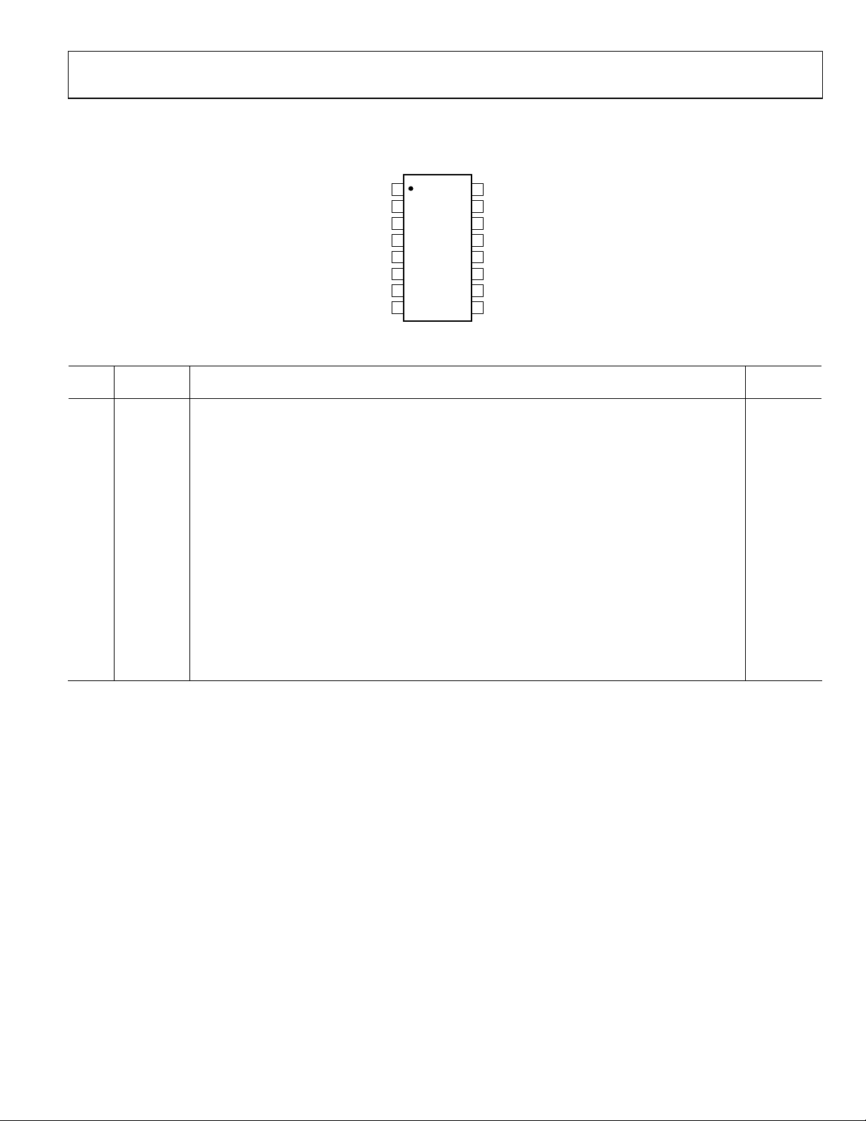
PIN CONFIGURATION AND FUNCTION DESCRIPTION
COMM
CHPF
DECL
INHI
INLO
DECL
PWDN
COMM
1
2
3
AD8362
4
TOP VIEW
5
(Not to Scale)
6
7
8
16
15
14
13
12
11
10
9
ACOM
VREF
VTGT
VPOS
VOUT
VSET
ACOM
CLPF
02923-B-002
Figure 2. Pin Configuration
Table 3. Pin Function Descriptions
Pin
No.
Mnemonic Description
Equivalent
Circuit
1, 8 COMM Common Connection. Connect via low impedance to system common.
2 CHPF Input HPF. Connect to common via a capacitor to determine 3 dB point of input signal high-pass filter.
3, 6 DECL
Decoupling Terminals for INHI and INLO. Connect to common via a large capacitance to complete
input circuit.
4 INHI High Signal Input Terminal. Part of a differential input port with INLO. Circuit A
5 INLO Low Signal Input Terminal. Part of a differential input port with INHI. Circuit A
7 PWDN Disable/Enable Control Input. Apply logic high voltage to shut down the AD8362.
9 CLPF
Connection for loop filter integration (averaging) capacitor, the other pin of which is usually
grounded via a resistor to improve loop stability and response time.
10, 16 ACOM Analog Common Connection for Output Amplifier.
11 VSET
The voltage applied to this pin sets the decibel value of the required RF input voltage that results in
Circuit B
zero current out of CLPF and thus the loop integrating capacitor.
12 VOUT Output of Error Amplifier. In measurement mode, normally connected directly to VSET. Circuit C
13 VPOS Connect to 5 V Power Supply.
14 VTGT
The logarithmic intercept voltage is proportional to the voltage applied to this pin. The use of a lower
Circuit D
target voltage increases the crest factor capacity.
15 VREF General-Purpose Reference Voltage Output of 1.25 V (usually connected only to VTGT). Circuit E
Rev. B | Page 7 of 36
AD8362
EQUIVALENT CIRCUITS
DECL
INHI
INLO
DECL
COMM
100Ω
VGA
100Ω
VPOS
Figure 3. Circuit A
VPOS
COMM
VPOS
VSET
ACOM
COMM
~35kΩ
~35kΩ
VSET
INTERFACE
RAIL-TO-RAIL
0.7V
CLPF
02923-B-004
OUTPUT
2kΩ
500Ω
Figure 6. Circuit D
VPOS
VOUT
ACOM
COMM
02923-B-006
Figure 4. Circuit B
SOURCE ONLY
VPOS
02923-B-003
VTGT
ACOM
COMM
50kΩ
50kΩ
VTGT
INTERFACE
GAIN = 0.12
02923-B-005
~0.35V
REF BUF
13kΩ
5kΩ
Figure 7. Circuit E
Figure 5. Circuit C
VPOS
VOUT
ACOM
COMM
02923-B-007
Rev. B | Page 8 of 36
AD8362
TYPICAL PERFORMANCE CHARACTERISTICS
4.5
4.0
3.5
3.0
2.5
2.0
VOUT (V)
1.5
1.0
0.5
0
–60
–55 –50 –45 –40 –35 –30 –25 –20 –15 –5 0 5 10
900MHz
1900MHz
INPUT AMPLITUDE (dBm)
2200MHz
2700MHz
–10
100MHz
15
02923-B-008
4.0
3.6
3.2
2.8
2.4
2.0
VOUT (V)
1.6
+25°C
1.2
–40°C
0.8
0.4
0
–60–55 –50 –45 –40 –35 –30 –25 –20 –15 –5 0 5 10 15–10
–40°C
+85°C
+25°C
+85°C
INPUT AMPLITUDE (dBm)
3.0
2.4
1.8
1.2
0.6
0
–0.6
–1.2
ERROR IN VOUT (dB)
–1.8
–2.4
–3.0
02923-B-011
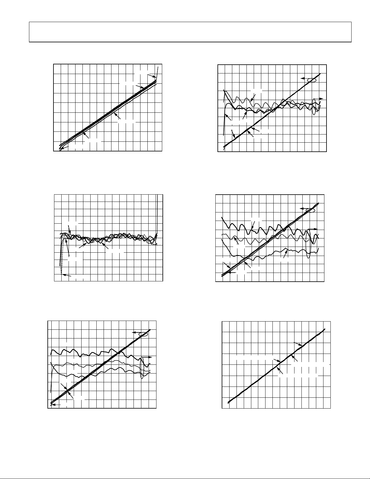
Figure 8. Output Voltage (VOUT) vs. Input Amplitude (dBm),
Frequencies 100 MHz, 900 MHz, 1900 MHz, 2200 MHz, 2700 MHz,
Sine Wave, Differential Drive
3.0
2.5
2.0
1.5
100MHz
1.0
0.5
0
–0.5
–1.0
ERROR IN VOUT (dB)
–1.5
–2.0
–2.5
–3.0
–60
2200MHz
900MHz
2700MHz
–55 –50 –45 –40 –35 –30 –25 –20 –15 –5 0 5 10
INPUT AMPLITUDE (dBm)
1900MHz
–10
Figure 9. Logarithmic Law Conformance vs. Input Amplitude
Frequencies 100 MHz, 900 MHz, 1900 MHz, 2200 MHz, 2700 MHz,
Sine Wave, Differential Drive
4.0
3.6
3.2
2.8
2.4
2.0
VOUT (V)
1.6
1.2
0.8
0.4
–40°C
+25°C
+85°C
–40°C
+85°C
+25°C
0
–55
–50 –45 –40 –35 –30 –25 –20 –15 –5 0 5 10
INPUT AMPLITUDE (dBm)
–10
15
3.0
2.4
1.8
1.2
0.6
0
–0.6
–1.2
–1.8
–2.4
–3.0
15
02923-B-009
ERROR IN VOUT (dB)
02923-B-010
Figure 11. VOUT and Law Conformance vs. Input Amplitude, Frequency
1900 MHz, Sine Wave, Temperature −40°C, +25°C, and +85°C
4.0
3.6
3.2
2.8
2.4
2.0
VOUT (V)
1.6
1.2
–40°C
0.8
0.4
0
–50 –45 –40 –35 –30 –25 –20 –15 –5 0 5 10
–60
–55
–40°C
+25°C
+85°C
+25°C
INPUT AMPLITUDE (dBm)
+85°C
–10
3.0
2.4
1.8
1.2
0.6
0
–0.6
–1.2
–1.8
–2.4
–3.0
15
Figure 12. VOUT and Law Conformance vs. Input Amplitude, Frequency
2200 MHz, Sine Wave, Temperature −40°C, +25°C, and +85°C
4.0
3.5
3.0
2.5
2.0
VOUT (V)
1.5
1.0
0.5
0
IS95 REVERSE LINK
–55 –50 –45 –40 –35 –30 –25 –20 –15 –5 0 5 10
–60
INPUT AMPLITUDE (dBm)
CW
WCDMA 8-CHANNEL
WCDMA 15-CHANNEL
–10
15
ERROR IN VOUT (dB)
02923-B-012
02923-B-013
Figure 10. VOUT and Law Conformance vs. Input Amplitude, Frequency
900 MHz, Sine Wave, Temperature −40°C, +25°C, and +85°C
Figure 13. VOUT vs. Input Amplitude with Different Waveforms, CW, IS95
Reverse Link, WCDMA 8-Channel, WCDM 15- Channel, Frequency 900 MHz
Rev. B | Page 9 of 36
AD8362
3.0
2.5
2.0
1.5
WCDMA 8-CHANNEL
–10
WCDMA
8-CHANNEL
WCDMA 8-CHANNEL
WCDMA 15-CHANNEL
–10
–0.5
–1.0
ERROR IN VOUT (dB)
–1.5
–2.0
–2.5
–3.0
1.0
0.5
0
–60
IS95 REVERSE LINK
CW
WCDMA 15-CHANNEL
–55 –50 –45 –40 –35 –30 –25 –20 –15 –5 0 5 10
INPUT AMPLITUDE (dBm)
Figure 14. Output Error from CW Linear Reference vs. Input Amplitude
with Different Waveforms, CW, IS95 Reverse Link, WCDMA 8-Channel,
WCDMA 15-Channel, Frequency 900 MHz
3.0
2.5
2.0
1.5
1.0
0.5
0
–0.5
–1.0
ERROR IN VOUT (dB)
–1.5
–2.0
–2.5
–3.0
–55 –50 –45 –40 –35 –30 –25 –20 –15 –5 0 5 10–10
WCDMA
4-CHANNEL
C
W
WCDMA 15-CHANNEL
INPUT AMPLITUDE (dBm)
Figure 15. Output Error from CW Linear Reference vs. Input Amplitude
with Different WCDMA Channel Loading, 4-Channel, 8-Channel,
15-Channel, Frequency 2200 MHz
3.0
2.5
2.0
1.5
1.0
0.5
0
–0.5
–1.0
ERROR IN VOUT (dB)
–1.5
–2.0
–2.5
–3.0
–60
–55 –50 –45 –40 –35 –30 –25 –20 –15 –5 0 5 10
INPUT AMPLITUDE (dBm)
Figure 16. Output Error from CW Linear Reference vs. Input Amplitude,
3 Sigma to Either Side of Mean, with WCDMA 8-Channel,
WCDMA 15-Channel, Frequency 1900 MHz
3.0
2.5
2.0
1.5
1.0
0.5
–0.5
–1.0
ERROR IN VOUT (dB)
–1.5
–2.0
–2.5
15
02923-B-014
–3.0
WCDMA
8-CHANNEL
0
WCDMA
15-CHANNEL
–55 –50 –45 –40 –35 –30 –25 –20 –15 –5 0 5 10
–60
INPUT AMPLITUDE (dBm)
–10
15
02923-B-017
Figure 17. Output Error from CW Linear Reference vs. Input Amplitude,
3 Sigma to Either Side of Mean, with WCDMA 8-Channel,
15-Channel, Frequency 1900 MHz
3.0
2.5
2.0
WCDMA
8-CHANNEL
1.5
1.0
0.5
0
–0.5
–1.0
ERROR IN VOUT (dB)
–1.5
–2.0
–2.5
–3.0
–55 –50 –45 –40 –35 –30 –25 –20 –15 –5 0 5 10
02923-B-015
–60
WCDMA
15-CHANNEL
INPUT AMPLITUDE (dBm)
–10
15
02923-B-018
Figure 18. Output Error from CW Linear Reference vs. Input Amplitude,
3 Sigma to Either Side of Mean, with WCDMA 8-Channel,
WCDMA 15-Channel, Frequency 2200 MHz
4.0
3.5
3.0
2.5
2.0
VOUT (V)
1.5
1.0
0.5
0
15
02923-B-016
–55 –50 –45 –40 –35 –30 –25 –20 –15 –5 0 5 10
INPUT AMPLITUDE (dBm)
–10
02923-B-019
Figure 19. VOUT vs. Input Amplitude, 3 Sigma to Either Side of Mean,
Sine Wave, Frequency 900 MHz, Part-to-Part Variation
Rev. B | Page 10 of 36
AD8362
4.0
3.5
3.0
2.5
2.0
VOUT (V)
1.5
1.0
0.5
0
–55 –50 –45 –40 –35 –30 –25 –20 –15 –5 0 5
INPUT AMPLITUDE (dBm)
–10
10
Figure 20. VOUT vs. Input Amplitude, 3 Sigma to Either Side of Mean,
Sine Wave, Frequency 1900 MHz, Part-to-Part Variation
3.0
2.5
2.0
1.5
1.0
0.5
0
–0.5
–1.0
ERROR IN VOUT (dB)
–1.5
–2.0
–2.5
–3.0
–55
–50 –45 –40 –35 –30 –25 –20 –15 –5 0 5 10
–40°C
+25°C
INPUT AMPLITUDE (dBm)
+85°C
–10
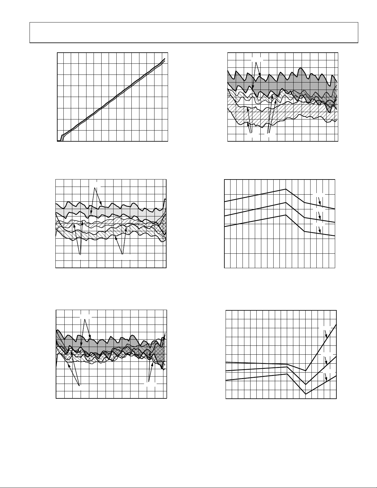
Figure 21. Logarithmic Law Conformance vs. Input Amplitude,
3 Sigma to Either Side of Mean, Sine Wave, Frequency 900 MHz,
Temperature −40°C, +25°C, and +85°C
3.0
2.5
2.0
1.5
1.0
0.5
0
–0.5
–1.0
ERROR IN VOUT (dB)
–1.5
–2.0
–2.5
–3.0
–55
–50 –45 –40 –35 –30 –25 –20 –15 –5 0 5 10
–45°C
+85°C
INPUT AMPLITUDE (dBm)
+25°C
–10
02923-B-022
Figure 22. Logarithmic Law Conformance vs. Input Amplitude,
3 Sigma to Either Side of Mean, Sine Wave, Frequency 1900 MHz,
Temperature −40°C, +25°C, and +85°C
02923-B-020
02923-B-021
3.0
2.5
2.0
1.5
1.0
0.5
0
–0.5
–1.0
ERROR IN VOUT (dB)
–1.5
–2.0
–2.5
–3.0
–55
–50 –45 –40 –35 –30 –25 –20 –15 –5 0 5 10
–40°C
+85°C
+25°C
INPUT AMPLITUDE (dBm)
–10
Figure 23. Logarithmic Law Conformance vs. Input Amplitude,
3 Sigma to Either Side of Mean, Sine Wave, Frequency 2200 MHz,
Temperature −40°C, +25°C, and +85°C
52.0
SLOPE (mV)
51.5
51.0
50.5
50.0
49.5
49.0
900
1000
1100
1200
1300
1400
1500
1600
1700
FREQUENCY (MHz)
1800
1900
2000
2100
2200
+85°C
+25°C
–40°C
2300
2400
2500
2600
Figure 24. Logarithmic Slope vs. Frequency,
Temperature −40°C, +25°C, and +85°C
–53
–54
–55
–56
–57
–58
–59
INTERCEPT (dBm)
–60
–61
–62
–63
900
1000
1100
1200
1300
1400
1500
1600
1700
1800
FREQUENCY (MHz)
1900
2000
2100
2200
2300
+85°C
+25°C
–40°C
2400
2500
2600
Figure 25. Logarithmic Intercept vs. Frequency,
Temperature −40°C, +25°C, and +85°C
2700
2700
02923-B-023
02923-B-024
02923-B-025
Rev. B | Page 11 of 36

AD8362
3.0
2.5
2.0
CHANGE IN SLOPE (mV)
1.5
1.0
0.5
–0.5
–1.0
–1.5
–2.0
–2.5
–3.0
0
–40
1900MHz
2200MHz
–30 –20 –10 0 10 20 30 40 50 70 80 90
TEMPERATURE (°C)
Figure 26. Change in Logarithmic Slope vs. Temperature, 3 Sigma to Either
Side of Mean, Frequencies 900 MHz, 1900 MHz, 2200 MHz
2.0
1.5
1.0
0.5
–0.5
–1.0
CHANGE IN INTERCEPT (dB)
–1.5
–2.0
1900MHz
0
2200MHz
–40
900MHz
–30 –20 –10 0 10 20 30 40 50 70 80 90
TEMPERATURE (°C)
Figure 27. Change in Logarithmic Intercept vs. Temperature, 3 Sigma to
Either Side of Mean, Frequencies 900 MHz, 1900 MHz, 2200 MHz
100
80
60
HITS
40
20
0
48 5349 50 51 52
SLOPE (mV/dB)
Figure 28. Slope Distribution, Frequency 900 MHz
900MHz
60
60
80
70
60
50
40
HITS
30
20
10
0
–61.0 –58.0–60.5 –60.0 –59.5 –59.0 –58.5
02923-B-026
INTERCEPT (dBm)
02923-B-029
Figure 29. Logarithmic Intercept Distribution, Frequency 900 MHz
5.0
4.5
4.0
3.5
3.0
2.5
VOUT (V)
2.0
1.5
1.0
0.5
0
02923-B-027
F
R
S
T
R
U
B
L
B
A
E
E
N
d
2
m
+
B
T
U
V
O
.
0
V
/
5
I
D
V
2101420
0
46
–10dBm
–20dBm
–30dBm
812 1816
TIME (µs)
2V/
I
D
V
6
4
2
0
–2
–4
–6
–8
–10
–12
–14
RF BURST ENABLE (V)
02923-B-030
Figure 30. Output Response to RF Burst Input for Various
RF Input Levels, Carrier Frequency 900 MHz, CLPF = 0.1 µF
5.0
4.5
4.0
3.5
3.0
2.5
VOUT (V)
2.0
1.5
1.0
0.5
02923-B-028
F
R
S
T
R
U
B
L
B
A
E
E
N
d
2
m
+
B
–10dBm
V
O
T
U
.
0
5V/
I
D
V
0
2101420
0
46
–20dBm
–30dBm
812 1816
TIME (ms)
V
2
6
4
/
I
D
V
2
0
–2
–4
–6
–8
RF BURST ENABLE (V)
–10
–12
–14
02923-B-031
Figure 31. Output Response to RF Burst Input for Various RF Input Levels,
Carrier Frequency 900 MHz, CLPF = 0.1 µF
Rev. B | Page 12 of 36

AD8362
5.0
4.5
4.0
3.5
3.0
2.5
VOUT (V)
2.0
1.5
1.0
0.5
0
-
E
R
P
O
W
O
D
W
N
P
I
N
+
d
2
m
V
O
T
U
.
0
V
/
5
I
D
V
2101420
0
46
812 1816
B
–10dBm
–20dBm
–30dBm
TIME (µs)
6
4
V
/
2
I
D
V
2
0
–2
–4
–6
–8
POWER-DOWN PIN (V)
–10
–12
–14
Figure 32. Output Response Using Power-Down Mode for Various RF Input
Levels, Carrier Frequency 900 MHz, CLPF = 0
5.0
4.5
4.0
3.5
3.0
2.5
VOUT (V)
2.0
1.5
I
V
.
0
V
/
5
D
1.0
0.5
0
2101420
0
46
+
d
2
m
B
–10dBm
–20dBm
–30dBm
812 1816
TIME (ms)
6
4
V
/
2
I
D
V
2
0
–2
–4
–6
–8
POWER-DOWN PIN (V)
–10
–12
–14
Figure 33. Output Response Using Power-Down Mode for Various RF Input
Levels, Carrier Frequency 900 MHz, CLPF = 0.1 µF
5.5
5.0
4.5
4.0
3.5
3.0
VOUT (V)
2.5
2.0
1.5
1.0
0
V
/
1
D
2101420
0
I
V
46
VPOS
812 1816
TIME (ms)
2
d
2
+
B
–10dBm
–20dBm
–30dBm
V
6
4
/
I
D
V
2
0
–2
–4
–6
m
–8
POWER-DOWN PIN (V)
–10
–12
–14
Figure 34. Output Response to Gating on Power Supply for Various RF Input
Levels, Carrier Frequency 900 MHz, CLPF = 0
120
150
210
240
02923-B-032
Figure 35. Input Impedance, Z
5
0
–5
–10
–15
CHANGE IN VREF (mV)
–20
–25
–30
–30 –20 –10 0 10 20 30 40 50 70 80 90
02923-B-033
–40
Figure 36. Change in VREF vs. Temperature, 3 Sigma to Either Side of Mean
300
250
200
HITS
150
100
50
0
02923-B-034
1.230 1.2701.235 1.240 1.245 1.250 1.2601.255 1.265
Figure 37. VREF Distribution
90
270
= 50 Ω, Differential Drive
O
TEMPERATURE (°C)
VREF (V)
60
300
30
0180
330
02923-B-035
60
02923-B-036
02923-B-037
Rev. B | Page 13 of 36

AD8362
(
)
CHARACTERIZATION SETUP
EQUIPMENT
The general hardware configuration used for most of the
AD8362 characterization is shown in Figure 38. The signal
source used was a Rohde & Schwarz SMIQ03B. A 1:4 balun
transformer was used to transform the single-ended RF signal
to differential form. For the response measurements in Figure
30 and Figure 31, the configuration shown in Figure 39 was
used; for Figure 32 and Figure 33, the configuration shown in
Figure 40 was used; and for Figure 34, the configuration shown
in Figure 41 was used.
AD8362
CHARACTERIZATION
SMIQ03B
RF SOURCE
3dB
RFIN
BOARD
VOUT
MULTIMETER
HP34401A
TEK TDS5104
SCOPE
SMT03
SIGNAL
GENERATOR
RF 50Ω
TEK P5050
VOLTAGE PROBE
BALUN
3dB
C2
AD8362
COMM
CHPF
C1
DECL
INHI
INLO
DECL
C3
PWDN
COMM
Figure 39. Response Measurement Setup for Modulated Pulse
ACOM
VREF
VTGT
VPOS
VOUT
VSET
ACOM
CLPF
HPE3631A
POWER
SUPPLY
C4
02923-B-039
PC
CONTROLLER
Figure 38. Primary Characterization Setup
ANALYSIS
The slope and intercept are derived using the coefficients
of a linear regression performed on data collected in its
central operating range. Error is stated in two forms: error
from linear response to CW waveform and output delta
from 25°C performance.
The error from linear response to CW waveform is the
decibel difference in output from the ideal output defined by
the conversion gain and output reference. This is a measure of
the linearity of the device response to both CW and modulated
waveforms. The error in dB is calculated by
−×−
PPSlopeVOUT
IN
()
=dB
Slope
is the x intercept, expressed in dBm.
where
Error
P
Z
Error from the linear response to CW waveform is not a
measure of absolute accuracy since it is calculated using the
slope and intercept of each device. However, it verifies the
linearity and the effect of modulation on the device response.
Error from 25°C performance uses the performance of a given
device and waveform type as the reference; it is predominantly a
measurement of output variation with temperature.
Z
02923-B-038
TEK TDS5104
SCOPE
SMT03
SIGNAL
GENERATOR
RF 50Ω
HP8112A
PULSE
GENERATOR
TEK P5050
VOLTAGE PROBE
BALUN
3dB
C2
AD8362
COMM
CHPF
C1
DECL
INHI
INLO
DECL
C3
PWDN
COMM
Figure 40. Response Measurement Setup for Power-Down Step
AD811
732Ω
AD8362
COMM
ACOM
CHPF
DECL
INHI
INLO
DECL
PWDN
COMM
VREF
VTGT
VPOS
VOUT
VSET
ACOM
CLPF
BALUN
3dB
SMT03
SIGNAL
GENERATOR
RF 50Ω
C1
C2
C3
Figure 41. Response Measurement Setup for Gated Supply
50Ω
0.01µF 100pF
C4
ACOM
VREF
VTGT
VPOS
VOUT
VSET
ACOM
CLPF
HP8112A
PULSE
GENERATOR
TEK TDS5104
SCOPE
HPE3631A
POWER
SUPPLY
C4
TEK P5050
VOLTAGE
PROBE
02923-B-040
02923-B-041
Rev. B | Page 14 of 36

AD8362
–
(
)
−
=
(
)
=
=
(
)
=
CIRCUIT DESCRIPTION
The AD8362 is a fully calibrated, high accuracy, rms-to-dc
converter providing a measurement range of over 60 dB. It is
capable of operation from signals as low in frequency as a few
Hertz to at least 2.7 GHz. Unlike earlier rms-to-dc converters,
the response bandwidth is completely independent of the signal
magnitude. The −3 dB point occurs at about 3.5 GHz. The
capacity of this part to accurately measure waveforms having a
high peak-to-rms ratio (crest factor) is independent of either
the signal frequency or its absolute magnitude, over a wide
range of conditions.
This unique combination allows the AD8362 be to used with
equal ease as a calibrated RF wattmeter covering a power ratio
of >1,000,000:1, as a power controller in closed-loop systems, or
as a general-purpose rms-responding voltmeter, and in many
other low frequency applications.
AMPLITUDE TARGET
25dB TO +43dB
INHI
INLO
CHPF
OFFSET
NULLING
V
SET
VSET
V
REF
VREF
1.25V
MATCH WIDE-
BAND SQUARERS
V
SIG
I
SQUITGT
G
SET
CLPF
EXTERNAL
2
X
C
LPF
VGA
SETPOINT
INTERFACE
BAND GAP
REFERENCE
Figure 42. Basic Structure of the AD8362
FOR V
SIG
2
× 0.06
X
V
ATG
C
F
OUTPUT
FILTER
INTERNAL RESISTORS
SET BUFFER GAIN TO 5
V
V
OUT
TGT
VTGT
ACOM
VOUT
ACOM
02923-B-042
The part comprises the core elements of a high performance
AGC loop (Figure 42), laser-trimmed during manufacture to
close tolerances while fully operational at a test frequency of
100 MHz. Its linear, wideband, variable gain amplifier (VGA)
provides a general voltage gain, G
; this may be controlled in a
SET
precisely exponential (linear-in-dB) manner over the full 68 dB
range from −25 dB to +43 dB by a voltage V
. However, to
SET
provide adequate guard-banding, only the central 60 dB of this
range, from −21 dB to +39 dB, is normally used. Later, it is
shown how this basic range may be shifted either up or down,
and even extended to >80 dB. The VGA gain has the form
VVSETGG
GNSO
is a scaling voltage that
GNS
where
SET
G
exp (1)
is a basic fixed gain and V
O
defines the gain slope (the dB change per volt). Note that the
gain decreases with V
SIG
SET
where V
is the ac voltage applied to the input terminals
IN
. The VGA output is
SET
IN
IN
O
VVSETVGVGV exp
(2)
GNS
of the AD8362.
As is later explained more fully, the input drive may be
either single-sided or differential but optimum performance at
input drive. The effect of HF imbalances when using a singlesided drive is less apparent at low frequencies (from 50 Hz
to 500 MHz), but the peak input voltage capacity is always
halved relative to differential operation (see the Using the
AD8362 section).
SQUARE-LAW DETECTION
The output of the variable-gain amplifier, V
applied to a wideband square law detector, which provides a
true rms response to this alternating signal that is essentially
independent of waveform up to crest factors of 6. Its output
is a fluctuating current, I
, having a positive mean value. This
SQU
current is integrated by an on-chip capacitance, C
usually augmented by an external capacitance, CLPF, to extend
the averaging time. The resulting voltage is buffered by a gainof-5, dc-coupled amplifier whose rail-to-rail output, VOUT, may
be used either for measurement or control purposes.
In most applications, the AGC loop is closed via the setpoint
interface pin, VSET, to which the VGA gain-control voltage
VSET is applied. In measurement modes, the closure is direct
and local by a simple connection from the output the VOUT
pin to the VSET pin. In controller modes, the feedback path is
around some larger system, but the operation is the same.
The fluctuating current, I
target current, I
, using current mode subtraction. With the
TGT
, is balanced against a fixed setpoint
SQU
exact integration provided by the capacitor(s), the AGC loop
equilibrates when
IIMEAN
SQU
(3)
TGT
SIG
, is
; this is
F
The current I
cell whose input is the amplitude-target voltage V
is provided by a second-reference squaring
TGT
. This is a
ATG
fraction of the voltage VTGT applied to a special interface that
accepts this input at the VTGT pin. Since the two squaring cells
are electrically identical and are carefully implemented in the
IC, process and temperature-dependent variations in the
detailed behavior of the two square-law functions cancel.
Rev. B | Page 15 of 36

AD8362
(
)
(
)
[
]
[
]
(
)
[
]
[
]
Accordingly, VTGT (and its fractional part V
) determines the
ATG
output that must be provided by the VGA for the AGC loop to
settle. Since the scaling parameters of the two squarers are
accurately matched, it follows that Equation 3 is satisfied only
when
()
SIG
22
VVMEAN = (4)
ATG
In a formal solution, one would then extract the square root of
both sides to provide an explicit value for the root-mean-square
(rms) value. However, it is apparent that by forcing this identity,
through varying the VGA gain and extracting the mean value
by the filter provided by the capacitor(s), the system inherently
establishes the relationship
VVrms = (5)
SIG
ATG
Substituting the value of V
IN
O
As a measurement device, V
from Equation 2, we have
SIG
VVVSETVGrms =−exp (6)
GNS
is the unknown quantity and all
IN
ATG
other parameters can be fixed by design. Solving Equation 6:
IN
O
ATG
VVSETVVGrms exp= (7)
GNS
so
()
VVrmsVVSET log= (8)
GNS
The quantity V
= V
Z
ATG/GO
because VSET must be 0 when rms (V
IN
Z
is defined as the intercept voltage
) = VZ.
IN
When connected as a measurement device, the output of the
buffer is tied directly to VSET, which closes the AGC loop.
Making the substitution VOUT = VSET and changing the log
base to 10, as needed in a decibel conversion, we have
()
VVrmsVVOUT
IN
Z
where V
log= (9)
10
SLP
is the slope voltage, that is, the change in output
SLP
voltage for each decade of change in the input amplitude.
(Note that V
V
is laser trimmed to 1 V using a 100 MHz test signal.
SLP
SLP
= V
log (10) = 2.303 V
GNS
). In the AD8362,
GNS
Because a decade corresponds to 20 dB, this slope may also be
stated as 50 mV/dB. It is later shown how the effective value of
V
may be altered by the user.
SLP
Likewise, the intercept V
is also laser trimmed to 316 µV
Z
(−70 dBV). In an ideal system, VOUT would cross zero for an
rms input of that value. In a single-supply realization of the
function, VOUT cannot run fully down to ground; here, V
is
Z
the extrapolated value. In measurement modes, the output
ranges from 0.5 V for V
= 1 mV (input values are stated as
IN
rms, outputs values as dc), up to a voltage 60 dB × 50 mV/dB =
3 V above this for V
= 1 V, that is, to 3.5 V. Figure 43 shows the
IN
ideal form of Equation 9 scaled as in the AD8362.
4.0
3.5
3.0
2.5
2.0
1.5
OUTPUT VOLTAGE (V)
1.0
0.5
0
100µV
1mV 10mV 100mV 1V 10V
RMS INPUT VOLTAGE (100µV TO 3.2V)
Figure 43. Ideal Response of the AD8362
02923-B-043
EFFECT OF INPUT COUPLING ON THE INTERCEPT VALUE
Reductions of VIN due to coupling losses directly affect VZ. In
high frequency applications, several factors contribute to the
coupling of the source into the IC, including the board and
package resonances and attenuation. Any uncertainties in the
input impedance result in the intercept expressed in power
terms, which is nominally −57 dBm for a 50 Ω system, being
less accurately determined than when stated in dBV (that is, in
pure voltage) terms. On the other hand, the slope V
SLP
is
unaffected by all such impedance or coupling uncertainties.
OFFSET ELIMINATION
To address the small dc offsets that arise in the variable gain
amplifier, an offset-nulling loop is used. The high-pass corner
frequency of this loop is internally preset to 1 MHz, sufficiently
low for most HF applications. When using the AD8362 in LF
applications, the corner frequency can be reduced as needed by
the addition of a capacitor from the CHPF pin to ground having
a nominal value of 200 µF/Hz. For example, to lower the highpass corner frequency to 150 Hz, a capacitance of 1.33 µF is
required. The offset voltage varies depending on the actual gain
at which the VGA is operating, and thus, on the input signal
amplitude.
Baseline variations of this sort are a common aspect of all
VGAs, although more evident in the AD8362 because of the
method of its implementation, which causes the offsets to
ripple along the gain axis with a period of 6.33 dB. When an
excessively large value of CHPF is used, the offset correction
process may lag the more rapid changes in the VGA’s gain,
which may increase the time required for the loop to fully settle
for a given steady input amplitude.
Rev. B | Page 16 of 36

AD8362
(
)
VOLTAGE VS. POWER CALIBRATION
The AD8362 can be used as an accurate rms voltmeter
from arbitrarily low frequencies to microwave frequencies.
For low frequency operation, the input is usually specified
either in volts rms or in dBV (decibels relative to 1 V rms).
Driven differentially, the specified input range in dBV runs
from −60 dBV to 0 dBV (1 mV to 1 V rms). In these terms,
the intercept is at −70 dBV.
At high frequencies, signal levels are commonly specified
in power terms. In these circumstances, the source and
termination impedances are an essential part of the overall
scaling. To set the AD8362’s input impedance to 50 Ω, it is
necessary to add a resistor of 66.7 Ω across the internal 200 Ω
differential input impedance of the IC. (This is discussed
further in later sections.) For this condition, the intercept
occurs at a nominal power level of −57 dBm, and VOUT
can be stated in this way:
dBmV5057 ×+=INPVOUT (10)
where P
is expressed in dBm. For example, an input of
IN
−30 dBm generates an output of 1.35 V.
EFFECT OF SIGNAL WAVEFORM
The measurement accuracy of an rms-responding device is
ideally unaffected by the waveform of the input signal. This is a
valuable asset in wideband CDMA systems and in many other
modulation modes where there is a significant amount of
random variation of the RF carrier amplitude at baseband
frequencies. The high accuracy of the AD8362 in such cases is
indicated by the Typical Performance Characteristics graphs
and in the Specifications table. Note that at low frequencies, it is
customary to provide a specification of measurement errors due
to waveform effects as a function of the crest factor (σ) rather
than in terms of a system-specific modulation mode.
When measuring signals whose waveforms have high but
brief peak values (that is, having high crest factors), these
peaks may be clipped, causing a reduction in the apparent value
of the input being measured. This issue is discussed further in
connection with the detailed description of the input system.
OPE R ATIO N AT LOW FRE QUE NCI E S
In conventional rms-to-dc converters based on junction
techniques, the effective signal bandwidth is proportional to the
signal amplitude. For a 1 MHz rms-to-dc converter, this is the
full-scale bandwidth. However, at an input 60 dB below fullscale, the bandwidth could be as low as 1 kHz. In sharp contrast,
the 3.5 GHz bandwidth of the VGA in the AD8362 is
independent of its gain. Since this amplifier is internally dccoupled, the system can also be used as a high accuracy rms
voltmeter at low frequencies, retaining its temperature-stable
decibel-scaled output, for example, in seismic, audio, and sonar
instrumentation.
In such cases, the input coupling capacitors should be large
enough so that the lowest frequency components of the signal
that are to be included in the measurement are minimally
attenuated. For example, for a 3 dB reduction at 1.5 kHz,
capacitances of 1 µF are needed because the input resistance is
100 Ω at each input pin (200 Ω differentially) and we calculate
1/(2π × 1.5 kΩ × 100) = 1 µF. Also, to lower the high-pass
corner frequency of the VGA, a capacitor of value 200 µF-Hz
should be used between the CHPF pin and ground; to provide a
similar 1.5 kHz high-pass corner, a capacitor of 133 nF should
be used.
TIME-DOMAIN RESPONSE OF THE CLOSED LOOP
The external low-pass averaging capacitance, CLPF, added at
the output of the squaring cell, is chosen to provide adequate
filtering of the fluctuating detected signal. The optimum value
depends on the application; as a guideline, a value of roughly
900 µF-Hz should be used. For example, a capacitance of 5 µF
provides adequate filtering down to 180 Hz. Note that the
fluctuation in the quasi-dc output of a squaring cell operating
on a sine wave input is a raised cosine at twice the signal
frequency, easing this filtering function.
In the standard connections for the measurement mode,
the VSET pin is tied to VOUT. For small changes in input
amplitude (a few decibels), the time-domain response of this
loop is essentially linear, with a 3 dB low-pass corner frequency
of nominally f
around this local loop set the minimum recommended value of
this capacitor to about 300 pF, giving f
When large and abrupt changes of input amplitude occur,
the loop response becomes nonlinear and exhibits slew rate
limitations. Further, due to the fundamentals of a system using
transconductance squaring cells as employed in the AD8362,
the slewing is asymmetric for increasing and decreasing inputs.
Figure 44 shows typical waveforms for VOUT for three values
of V
using CLPF = 1 nF.
IN
3.0
2.8
2.6
2.4
2.2
2.0
1.8
1.6
1.4
1.2
1.0
OUTPUT VOLTAGE (V)
0.8
0.6
0.4
0.2
= 1/(CLPF × 1.1 kΩ). Internal time delays
LP
= 3 MHz.
LP
0
168 24324048566472808896
0
Figure 44. Typical Large-Scale Response
TIME (µs)
02923-B-044
Rev. B | Page 17 of 36

AD8362
The most satisfactory way to quantify slew-rate limitations is by
considering the peak currents that can be generated by the
squaring cells. During a fast increase in input level, the peak
current into the integrating (loop filter) capacitance, CLPF, is
approximately 2.5 mA. The actual value depends on several
factors, including the size of the step, and extremes in chip
temperature. The voltage across the 1 nF capacitor thus
increases at a rate of nominally 2.5 V/µs. Because the output
buffer has a gain of 5, the output slew rate is 12.5 V/µs. The peak
rate persists up to a point about 10 dB below the final value,
after which the response gradually converges on the linear
system response, as noted previously.
On the other hand, during a fast decrease in input level, the
peak current in CLPF in the opposite (discharging) direction is
much smaller; it is roughly 25 µA. Thus, the slew rate for VOUT
in the descending direction is only about 0.125 V/µs for CLPF =
1 nF. Discharging over the full 3 V range (a 60 dB reduction of
input) requires a time interval of ~24 µs. These figures are
verified in the results shown in Figure 44.
ALTERATION OF THE INTERNAL TARGET VOLTAGE
The AD8362 incorporates several features that extend its
versatility. One of these is the ability to alter the target
voltage. As noted, the output of the VGA is forced to a
value set by the internal bias voltage (V
applied to the reference squaring cell. It is normally set to 75
mV dc by connecting VTGT to the 1.25 V reference voltage at
the VREF pin. However, it may optionally be varied from 0 V
up to ±0.24 V (±4 V at VTGT). Note that the sign of this input
is unimportant, because it is internally squared.
By lowering V
, the output of the VGA needed to balance the
ATG
output currents of the two matched squaring cells is similarly
lowered. This reduces the intercept in precisely the same ratio.
Thus, if we halve the setpoint target voltage by halving the
voltage applied to the VTGT pin, the intercept moves to the left
(to a smaller input level) by 6.02 dB. This effectively doubles the
measurement system’s sensitivity.
Furthermore, because the signal amplitude needed to drive the
squaring cell is halved, the output stage of the VGA now has
twice the dynamic headroom (before clipping) and can handle
waveforms having crest factors that are twice as large. Figure 45
shows the overall response for an illustrative set of values of
VTGT = 0.3 V, 0.533 V, 0.949 V, 1.687 V, and 3.0 V. While this is
usually a fixed dc voltage, it can also be a time-varying, unipolar
or bipolar voltage, in which case the overall operation is rather
more complex. For example, when VTGT is derived from
VOUT
the dynamic range can be extended to over 80 dB.
,
Examples of such uses of this feature are presented later.
= 0.06 × VTGT)
ATG
3.7
3.2
2.7
2.2
1.7
1.2
0.7
OUTPUT VOLTAGE (V)
0.2
10
5
0
–5
–10
RELATIVE INTERCEPT (dB)
100µ 1m 10m 10
Figure 45. Response with VTGT Varied from 0.3 V to 3 V in 5 dB Steps,
VTGT = 300mV
VTGT = 533mV
VTGT = 949mV
VTGT = 1.69V
VTGT = 3.0V
0.1 1
RMS INPUT VOLTAGE (V)
Showing the Proportional Shift in Intercept
02923-B-045
EFFECTS AT EACH END OF DYNAMIC RANGE
All AGC loops have a limited minimum and maximum input
beyond which the system cannot respond correctly. However,
the output of a well-behaved system is in error in such a way as
to avoid anomalous measurements. For an input below its
minimum capability, the output should not turn around to
falsely indicate a higher input value; for inputs above its
maximum capability, the output should not fold over and return
to some lower value.
The actual behavior of the AD8362 under these conditions can
be seen in the set of plots in Figure 45, the lower panel of which
shows the deviation from the ideal response with a slope of
50 mV/dB. For inputs below a certain level corresponding to the
point at which the VGA is operating at its maximum gain, its
output can no longer meet the rms amplitude target set by
VTGT, so the output moves quickly to its minimum value in an
attempt to provide the needed extra gain. As VTGT is altered,
the corresponding end-limit voltage moves to the left or to the
right.
On the other hand, when the input is above a certain upper
limit where the VGA gain has been driven to its minimum
gain, any further increase drives its output well above the target
voltage needed to balance the loop. The resulting integration of
this internal error signal causes VOUT to rise abruptly. In either
case, this output takes on a safe value and does not fold back
under any conditions.
The dynamic range, the “dB distance” between these limits, is
not basically dependent on VTGT. The middle line in the plots
of Figure 45 (VTGT = 0.949 V) extends from 0.5 mV to 1.5 V
between the ±1% error points; the dynamic range is thus
slightly over 68 dB. For other values of VTGT, this basic 68 dB
range just moves to the left or to the right.
Rev. B | Page 18 of 36

AD8362
A
2
A
DECL
COMM
INHI
VIN
INLO
COMM
DECL
Figure 46. Input Protection at INHI and INLO Pins
VPOS
VPOS
VGA
02923-B-046
INPUT PROTECTION
Like all robust ICs, the AD8362 requires input protection
against high voltage transients at the input (ESD). However, the
techniques normally used for this purpose, based on breakdown
diodes from the input pins INHI and INLO to the supply pins
VPOS and COMM, cannot be used here because this raises the
risk of excessive signal coupling to internal nodes at the upper
end of the frequency range due to feedthrough in the
capacitances of these diodes. Package inductances cause all
internal nodes, including the supply and common lines, to have
a significant impedance back to the external ground plane; even
small disturbances on these nodes can cause anomalous
operation.
An unavoidable consequence of this method is that the diodes
will forward-conduct when the input amplitude is sufficient.
This is not an all-or-nothing effect, of course; they shunt the
input progressively as the signal increases. This conduction is
strongest at high temperatures when the forward drop voltage
of these diodes is lowest. The overall consequence is that high
amplitude peaks are clamped to a greater or lesser degree. This
affects the measurement accuracy at the top extreme of the
dynamic range whenever the signal waveform has a high crest
factor. These effects are, of course, included in the overall
performance specifications.
POWER-ENABLE RESPONSE TIME
The operating and standby currents for the AD8362 at 27°C
are 24 mA and 275 µA, respectively. The power-down mode
is activated by a logic high on the PWDN pin. When the
shutdown feature is used, the normal operating conditions
are restored relatively quickly when this pin is taken low.
Figure 47 shows typical response times for a midscale signal
(V
= 50 mV). The output rises to within 0.1 dB of its steady-
IN
state value in about 20 µs; the reference voltage is available to
full accuracy in a much shorter time. This wake-up response
varies in detail depending on the input coupling means and the
capacitances C
measurement system operating in the 0.8 GHz to 2 GHz range,
balun coupled at the input port, with C
and CLPF = 1 nF.
4.00m
10.00m
, CHPF, and CLPF. These results are for a
DEC
= 1 nF, CHPF = 0,
DEC
This risk is particularly evident because the main amplifier
in the AD8362’s VGA (an advanced X-AMP®) operates at full
gain under all conditions, while the signal input is variably
attenuated. Because this attenuation may be as high as 70 dB,
very small feedthrough effects in the 0.5 GHz to 3 GHz range
can have a pronounced impact on measurement accuracy.
Figure 46 shows the protection method used. The multiple
diodes arranged in back-to-back pairs limit the voltage swing
on the input pins by clamping to the two DECL pins, which
form a common ac low impedance node for the attenuators,
independently grounded via two external capacitors. The HF
currents in the capacitances of these diodes are thus shunted
directly to a signal null point.
Rev. B | Page 19 of 36
1.00mA
0.27mA
0.10mA
2.20V
2.19V
2.18V
1.26V
1.25V
1.24V
1dB
REFERENCE VOLTAGE
0
Figure 47. Typical Wake-Up Response; t
10 20 30 40
TIME (µs)
OUTPUT VOLTAGE
= 10 µs
0
02923-B-047

AD8362
USING THE AD8362
The AD8362 requires a single supply of nominally 5 V; its
performance is essentially unaffected by variations of up to
±10%, the range over which the stated specifications apply.
Supplies as low as 2.7 V may be used with some loss of
performance at high inputs and at temperature extremes.
The AD8362 is disabled by a logic high on the PWDN pin,
which may be directly grounded for continuous operation,
when the supply current at 27°C is nominally 24 mA and
essentially independent of supply voltage. When powered
down by a logic low on PWDN, the supply current is reduced
to about 275 µA.
BASIC CONNECTIONS
The supply is connected to the VPOS pin using the decoupling
network shown in Figure 48, whose capacitors must provide a
low impedance over the full frequency range of the input, and
should be placed as close as possible to the VPOS pin. Two
different capacitors are used in parallel to reduce the overall
impedance since these have different resonant frequencies.
However, the measurement accuracy is not critically dependent
on supply decoupling because the high frequency signal path is
confined to the relevant input pins. It is more important that the
lead lengths to INHI and INLO, and in the decoupling
capacitors from both of the DECL pins to ground, and the
connections from COMM to the ground plane all use the
shortest possible connections.
LOGIC HIGH FOR
SIGNAL INPUT
Z = 2 × 100Ω
1mV – 1V rms
POWER-DOWN
AD8362
COMM
1
CHPF
2
C
DEC
3
DECL
C
DEC
INHI
4
C
CPL
INLO
5
DECL
6
C
DEC
PWDN
7
COMM
8
ACOM
VREF
VTGT
VPOS
VOUT
VSET
ACOM
CLPF
16
15
14
13
12
11
10
Figure 48. Basic Measurement Mode Connections
V
S
+5V nom, @ 24mA
3.3Ω
0.1µF
1nF
V
9
C
LPF
OUT
02923-B-048
Rev. B | Page 20 of 36

AD8362
MAIN MODES OF OPERATION
V
Both measurement and controller modes are supported by the
AD8362. Typical connections for the measurement mode,
which may also be viewed as the rms voltmeter mode, are also
illustrated in Figure 48. The output, VOUT, is proportional to
the logarithm of the rms magnitude of the input signal (that is,
a linear-on-dB response). When used in an accurately known
system impedance (but only then), the output is a scaled decibel
measurement of the power represented by the input voltage.
The choice of the capacitances C
CPL
, C
, CHPF, and CLPF
DEC
depends on the lowest frequency to be included in the
measurement spectrum. The default values shown support
operation down to 100 Hz. Using a large enough value of CLPF
(10 µF) to ensure sufficient filtering at this low input frequency,
the response time is approximately 20 ms over most of the
dynamic range. In high frequency applications, this capacitor is
much smaller and is usually chosen to minimize the response
time, consistent with well-behaved, large-signal behavior. In this
figure, CHPF is also shown as 10 µF, to lower the high-pass
corner to about 90 Hz. However, no capacitor will be needed
here in most HF applications since the internally set high-pass
corner is at about 2 MHz.
Comparing the controller mode illustrated in Figure 49, the
AD8362 is used here to monitor the output of a variable gain
(or variable output power) signal processing element, frequently
a power amplifier, and adjust its output to a desired target value
(the setpoint) under the control of VSET. In this mode, its
function is somewhat like an RF comparator. With the path
from VOUT to VSET broken, any input larger than the
corresponding setpoint causes VOUT to rail to its maximum
value (which might loosely be viewed as a logic high). For
inputs smaller than the setpoint, the controller’s output falls to a
near-ground level (logic low). Using the AD8362 simply as a
threshold detector, this viewpoint may be useful, but in most
applications, it is an oversimplification. The AD8362 invariably
operates with the control loop closed, either locally with VOUT
connected to VSET (as in measurement mode), or globally via
some external nonlinear element (as in controller mode).
NC
1nF
1
2
3
4
5
6
7
8
AD8362
COMM
CHPF
DECL
INHI
INLO
DECL
PWDN
COMM
ACOM
VREF
VTGT
VPOS
VOUT
VSET
ACOM
CLPF
NO CONNECTION
FOR f >10MHz
SIGNAL INPUT
Z = 2 × 100Ω
1mV – 1V rms
THIS CONNECTION
SETS CHIP-ENABLE
1nF
C
CPL
Figure 49. Basic Controller Mode Connections
Controller mode operation is more closely analogous to that of
a classical proportional/integral/derivative (PID) loop. The
error corresponding to the decibel deviation from the setpoint
is integrated by current into a capacitor (the sum of the internal
and external capacitance CLPF) until such deviation is nulled.
This action provides the fundamental proportional part of the
loop response (although VOUT has decibel scaling). The Q of
this system can be adjusted to minimize the loop response time
by including a resistor in series with CLPF, generating a
transmission zero, which provides the derivative term of a
standard PID loop.
As a simple example, assume that the AD8362 operates at an
input power level of −20 dBm re: 50 Ω. Connected in the
measurement mode, it generates a VOUT of 2.00 V, because this
input is +40 dB above the intercept at −60 dBm and is scaled to
50 mV/dB. Rearranged to the controller mode with exactly this
voltage now externally applied to the VSET pin, the loop forces
VOUT to the control voltage required by the gain element to
provide a power sample of −20 dBm.
Of course, any control loop of this sort operates correctly
only if VSET corresponds to a power level (or a small sample of
such) that can actually be provided by the external gain element.
When this is a power amplifier, including the required amount
of RF attenuation ensures this condition. In certain instrumentation situations, it may be necessary to provide some low noise
gain ahead of the AD8362’s input.
S
+5V nom, @ 24mA
SETPOINT INPUT
0V–3.5V
300pF
3.3Ω
0.1µF
1nF
16
15
14
13
12
11
10
9
V
RAIL-TO-RAIL
OUT
CONTROL OUTPUT
02923-B-049
These two primary modes of use are discussed in more detail,
with emphasis on practical considerations.
Rev. B | Page 21 of 36

AD8362
(
)
OPERATION IN MEASUREMENT MODES
Figure 50 shows the general connections for operating the
AD8362 as an RF power detector, more correctly viewed
as an accurate measurement system. The full performance
potential of this part, particularly at very high frequencies
(above 500 MHz), is realized only when the input is presented
to the AD8362 in differential (balanced) form. In this example, a
flux-coupled transformer is used at the input. Having a 1:4
impedance ratio (1:2 turns ratio), the 200 Ω differential input
resistance of the AD8362 becomes 50 Ω at the input to the
transformer, whose outputs can be connected directly to INHI
and INLO. If a center-tapped transformer is used, connect the
tap to the DECL pins, which are biased to the same potential as
the inputs (~3.6 V). Over the 0.9 GHz to 2.2 GHz range, a
transmission line transformer (balun) may be used, as explained
later. (The evaluation board is supplied with a M/A-COM
ETC1.6-4-2-3, 0.5 GHz to 2.5 GHz, 4:1 balun.)
V
S
+5V nom, @ 24mA
1:4 Z-RATIO
(1:2 TURNS RATIO)
SIGNAL INPUT
Z = 50Ω
1nF
200Ω
Figure 50. Connections for RF Power Measurement
The output in this mode of use is a continuous, decibel-scaled
voltage ranging from about 0.5 V to 3.5 V.
IN
Z
The equivalent input power, P
above 1 mW) in a particular system impedance, which in this
case is 50 Ω. The intercept, P
the back-extrapolated output crosses zero. Expressed as a
voltage, it is 0.447 mV rms (−67 dBV, laser-calibrated at
100 MHz), corresponding to a P
However, the 1:2 turns ratio of the transformer halves the
required input voltage, which moves the intercept down by
6 dB to 0.224 mV rms (−73 dBV) at the transformer’s input.
AD8362
1
2
NC
3
4
5
6
1nF
7
8
50×= (11)
ACOM
VREF
VTGT
VPOS
VOUT
VSET
ACOM
CLPF
16
15
14
13
12
11
10
9
COMM
CHPF
DECL
INHI
INLO
DECL
PWDN
COMM
dBmVPPVOUT
, is expressed in dBm (decibels
IN
, is that input power for which
Z
of −60 dBm in 200 Ω.
Z
300pF
3.3Ω
0.1µF
1nF
V
RAIL-TO-RAIL
OUT
CONTROL OUTPUT
LAW CONFORMANCE ERROR
In practice, the response deviates slightly from the ideal straight
line suggested by Equation 11. This deviation is called the law
conformance error. In defining the performance of high
accuracy measurement devices, it is customary to provide plots
of this error. In general terms, it is computed by extracting the
best straight line to the measured data using linear regression
over a substantial region of the dynamic range and under
clearly specified conditions.
3.8
3.5
3.2
2.9
2.6
2.3
2.0
1.7
VOUT (V)
+
1.4
1.1
0.8
0.5
0.2
C
°
0
4
–
–60 –55 –50 –45 –40 –35 –30 –25 –20 –15 –5 0 5 10 15–10
C
°
0
4
–
C
°
5
2
C
+
°
5
8
5
8
+
INPUT AMPLITUDE (dBm)
C
°
5
2
+
C
°
Figure 51. Output Voltage and Law Conformance Error,
= −40°C, +25°C, and +85°C
at T
A
02923-B-050
Figure 51 shows the output of the circuit of Figure 50 over the
full input range. The agreement with the ideal function (law
conformance) is also shown. This was determined by linear
regression on the data points over the central portion of the
transfer function (35 mV to 250 mV rms) for the 25°C data.
The error at +25°C, −40°C, and +85°C was then calculated by
subtracting the ideal output voltage at each input signal level
from the actual output and dividing this quantity by the mean
slope of the regression equation to provide a measurement of
the error in decibels (scaled on the right-hand axis of Figure 51).
The error curves generated in this way reveal not only the
deviations from the ideal transfer function at a nominal
temperature but also all of the additional errors caused by
temperature changes. Notice there is a small temperature
dependence in the intercept (the vertical position of the error
plots); this variation is within 0.5 dB at high powers.
3.0
2.5
2.0
1.5
1.0
0.5
0
–0.5
–1.0
ERROR IN VOUT (dB)
–1.5
–2.0
–2.5
–3.0
02923-B-051
Impedance mismatches and attenuation in the coupling
elements significantly affect the intercept position. This error
is stable over temperature and time, and thus can be removed
during calibration in a specific system. The logarithmic slope of
50 mV/dB varies only slightly with frequency; corrected values
for several common frequencies are provided in the
Specifications section.
Figure 51 further reveals that there is a periodic ripple in the
conformance curves. This is due to the interpolation technique
used to select the signals from the attenuator, not only at
discrete tap points, but anywhere in between, thus providing
continuous attenuation values. The selected signal is then
applied to the 3.5 GHz, 40 dB fixed gain amplifier in the
remaining stages of the AD8362’s VGA.
Rev. B | Page 22 of 36

AD8362
E
A
An approximate schematic of the signal input section of the
AD8362 is shown in Figure 52. The ladder attenuator is
composed of 11 sections (12 taps), each of which progressively
attenuates the input signal by 6.33 dB. Each tap is connected to
a variable transconductance cell whose bias current determines
the signal weighting given to that tap. The interpolator
determines which stages are active by generating a discrete set
of bias currents, each having a Gaussian profile. These are
arranged to move from left to right, thereby determining the
attenuation applied to the input signal as the gain is
progressively lowered over the 69.3 dB range under control of
the VSET input. The detailed manner in which the
transconductance of adjacent stages varies as the virtual tap
point slides along the attenuator accounts for the ripple
observed in the conformance curves. Its magnitude is slightly
temperature dependent and also varies with frequency (see
Figure 10 to Figure 12). Notice that the system’s responses to
signal inputs at INHI and INLO are not completely
independent; these pins do not constitute a fully floating
differential input.
GUASSIAN INTERPOLATOR
gm gm gm gm
INHI
DECL
ATTENUATION
CONTROL
TO FIXED
GAIN STAGE
THIS INPUT
RF INPUT
Z = 50Ω
IS DRIVEN
1nF
R
SH
1nF
DECL AND
INLO ARE
NOT DRIVEN
NC
Figure 53. Input Coupling from a Single-Ended Source
Figure 53 illustrates one of many ways of coupling the signal
source to the AD8362. Because the input pins are biased to
about 3.6 V (for V
= 5 V) dc-blocking capacitors are required
S
when driving from a grounded source. For signal frequencies
>5 MHz, a value of 1 nF is adequate. While either INHI or
INLO may be used, INHI is chosen here, and INLO is
connected to the low side of the source. The resistor R
needed if a 100 Ω termination is acceptable. The corresponding
intercept is still −67 dBV, that is, 447 µV rms. However, specified
in power terms at 100 Ω, the P
Z
For a source termination of 50 Ω, the internal 100 Ω from INHI
to DECL must be shunted by a chip resistor of 100 Ω. At high
frequencies, a low attenuation pad at the input improves the
VSWR. For example, with a resistor of R
resistor of 25 Ω from the source to INHI, a termination of 50 Ω
is provided, with 6 dB of attenuation, raising the intercept to
−48 dBm.
1
2
3
4
5
6
7
8
AD8362
COMM
CHPF
DECL
INHI
INLO
DECL
PWDN
COMM
ACOM
VREF
VTGT
VPOS
VOUT
VSET
ACOM
CLPF
16
15
14
13
12
11
10
9
02923-B-053
is not
SH
is now at 2 nW or −57 dBm.
= 33 Ω and an added
SH
INLO
STAGE 1
6.33dB
STAGE 2
6.33dB
STAGE 11
6.33dB
Figure 52. Simplified Input Circuit
ALTERNATIVE INPUT COUPLING MEANS
The input stages of the AD8362 are optimally driven from a
fully balanced source, which should be provided wherever
possible. The ac low sides of both halves of the attenuator
internally connect to the DECL pin, which is therefore the RF
signal low terminal for both INHI and INLO. In many cases,
unbalanced sources can be applied directly to one or the other
of these two pins. The chief disadvantage of this driving method
is a reduction in dynamic range, particularly at very high
frequencies.
USING A NARROW-BAND INPUT MATCH
02923-B-052
While transformers offer the simplest method for providing
single-sided to balanced conversion, a good alternative is
using a specially designed narrow-band LC network, shown in
Figure 54, which also provides an input match. Using this basic
formulation, the match is to 50 Ω, with a voltage gain of 1.5
(3.56 dB) from the input connector to the AD8362. This
network is specially designed to provide a high degree of
amplitude balance at INHI and INLO as well as an exact phase
inversion. The narrow-band match provides a useful degree of
frequency selectivity, and the capacitors also serve to provide
the required dc blocking.
AD8362
1
COMM
2
NC
CHPF
RF INPUT
Z = 50Ω
THESE INPUTS ARE
EQUAL IN AMPLITUD
ND OF OPPOSITE SIGN
C1
C2
100Ω
L
3
4
5
6
7
8
DECL
INHI
INLO
DECL
PWDN
COMM
Figure 54. Narrow-Band Reactive Input Coupling
ACOM
VREF
VTGT
VPOS
VOUT
VSET
ACOM
CLPF
16
15
14
13
12
11
10
9
02923-B-054
Rev. B | Page 23 of 36

AD8362
(
)
=
(
)
=
The network can readily be scaled to other frequencies by
varying the product LC, while keeping the ratio L/C constant to
preserve a 50 Ω input impedance. Table 4 provides some spot
values; these take into account the reactive Z
of the AD8362.
IN
Table 4. Suggested Components for Narrow-Band 50 Ω
Match
Frequency (MHz) L (nH) C1 (pF) C2 (pF)
1 21850 2230 2765
2 10925 1115 1383
5 4370 446 553
10 2185 223 276
20 1093 112 138
50 437 45 55
100 220 22 27
200 100 10 12
500 40 3.9 4.7
This coupling method can be used down to much lower
frequencies than shown in Table 4 simply by multiplying the
1 MHz component values proportionally. The effects of the
reactive components of the AD8362’s inputs above 500 MHz
may require some fine tuning of the suggested values. In the
gigahertz region, the input coupling is usually more effectively
implemented using a balun.
UNCERTAINTIES IN R
AND POWER CALIBRATION
IN
In all the cases where a 50 Ω to 200 Ω transformation is
implemented, the voltage gain is only nominally ×2 (6 dB). This
ideal is impaired by the fact that the input resistances of the
AD8362 are not precise; variations of ±20% can be expected
from lot to lot. Therefore, it is necessary to use a calibration step
whenever an accurate value for the power intercept, P
, must be
Z
established.
CHOOSING THE RIGHT VALUE FOR CHPF AND CLPF
The AD8362’s 3.5 GHz variable gain amplifier includes an offset
cancellation loop, which introduces a high-pass filter effect in
its transfer function. The corner frequency, f
must be below that of the lowest input signal in the desired
measurement bandwidth frequency to properly measure the
amplitude of the input signal. The required value of the external
capacitor is given by
Thus, for operation at frequencies down to 100 kHz, CHPF
should be 2 nF.
In the standard connections for the measurement mode, the
VSET pin is tied to VOUT. For small changes in input amplitude
(a few decibels), the time-domain response of this loop is
essentially linear with a 3 dB low-pass corner frequency of
nominally f
this local loop set the minimum recommended value of this
capacitor to about 300 pF, making f
For operation at lower signal frequencies, or whenever the
averaging time needs to be longer, use
When the input signal exhibits large crest factors, such as a
WCDMA signal, CLPF must be much larger than might at
first seem necessary. This is due to the presence of significant
low frequency components in the complex, pseudo-random
modulation, which generates fluctuations in the output of
the AD8362.
, of this filter
HP
μF200
= 1/(CLPF × 1.1 kΩ). Internal time delays around
LP
μF900
HzinffCHPF
HPHP
LPLP
(12)
= 3 MHz.
LP
HzinffCLPF
(13)
When driven differentially, a significant improvement in
intercept accuracy can be achieved by shunting the 200 Ω
resistance from INHI to INLO with a 66.5 Ω resistor to set the
differential input resistance to 50 Ω. Assuming a tolerance of
±20% for the basic R
and ±1% for the chip resistor, the net
IN
input resistance could exhibit an error of ±2.5%. The resulting
error in P
(and thus in the absolute power measurement) may
Z
vary from −0.26 dB to +0.21 dB.
These precautions regarding input impedance do not apply
when the input is presented in voltage form, as is often the case
at low frequencies, or when the source impedance is low
compared to 200 Ω. For example, when using a feedback
amplifier as an impedance buffer ahead of the input, as in the
example in Figure 61, the loss at the interface at moderate
frequencies is negligible.
Rev. B | Page 24 of 36
USE OF NONSTANDARD TARGET VOLTAGES
An external connection between VREF and VTGT sets up
the internal target voltage, that is, the rms voltage that must
be provided by the VGA to balance the AGC feedback loop. In
the default scheme, the VREF of 1.25 V positions this target to
0.06 × 1.25 V = 75 mV. In principle, however, VTGT may be
driven by any voltage in the range −4 V to +4 V (the sign is
ignored) to alter this target, either in a fixed or dynamic way.
For example, if this pin is supplied from VREF via a simple
resistive attenuator of 1 kΩ:1 kΩ, the output required from the
VGA is halved (to 37.5 mV rms), which moves the nominal
intercept to −73 dBV. Under these conditions, the effective
headroom in the signal path that drives the squaring cell is
doubled. In principle, this doubles the peak crest factor that may
be handled by the system.
If VTGT is reduced too far, the accuracy and stability of the
intercept are compromised. The currents generated by the
transconductance mode squaring cells become smaller by the
square of the ratio. Thus, a factor of 5 reduction in VTGT

AD8362
(
lowers the signal currents in the squaring cells by a factor of 25.
As well as making the system more sensitive to small static
errors (offsets) in the postdetection circuitry, such a reduction
also reduces the peak slew rate. A suitable adjustment to the
value of CLPF is needed to maintain a given AGC loop
bandwidth. On the other hand, increasing the target voltage can
improve the accuracy and stability of the intercept for low crest
factor signals. Thus, using VTGT = 2.5 V, the peak output
currents of the squaring cell are quadrupled and the peak slew
rate is increased by the same factor. CLPF should be increased
to maintain an adequate stability margin in the AGC loop.
In many applications, it is useful to use a nonstandard value of
VTGT to shift the measurement range by a constant amount to
accommodate either a reduced or increased range of signal
inputs. The dynamic span remains >60 dB for such changes.
This technique is particularly useful when the sensitivity can be
lowered by raising VTGT, and there is little expectation of high
crest factor signals.
ADJUSTING THE INTERCEPT
Another way to take advantage of the effect of VTGT is to use it
to introduce an adjustment to the log intercept, represented by
the voltage V
terms of a modified value of V
A lower VTGT effectively increases the sensitivity of the
measurement system, which is just another way of stating that the
intercept moves to a lower value. This raises VOUT for all input
amplitudes, as demonstrated by the plots in Figure 45. This
control of the measurement system’s intercept could therefore be
brought about by applying the output of a DAC to the VTGT pin,
if that suits the overall objectives of an application.
For many purposes, a small manual adjustment range of ±3 dB
is sufficient. This can be implemented as shown in Figure 55.
Here, the largest fraction of VTGT is still provided by the builtin reference to minimize the sensitivity to supply voltage
variations. Now a variable component is provided by the trim
network. For a 5 V supply, this added component of VTGT is 0
when VR1 is centered. With the slider closest to ground, VTGT
is lowered by 366 mV, which corresponds to a 3 dB decrease in
intercept; in the opposite condition, it is raised by 518 mV,
which increases the intercept by 3 dB. That is, VTGT ranges
from 1.25 V/√2 to √2 × 1.25 V.
Other adjustment ranges can be readily calculated from this
example. The resistance at the VTGT pin is nominally 52 kΩ;
resistor values should be calculated with this in mind. In some
situations, this control interface might be driven from a
programmable source. In the simplest case, a logic level could
provide two intercept values, differing by say, 10 dB, thus
providing essentially two switched input ranges.
in Equation 14. Formally, this can be expressed in
Z
'.
Z
VVTGTVV
'
Z
Z
25.1= (14)
Also, it is worth remembering that these shifts in intercept are
equivalent, in most respects, to a dc offset applied to the
AD8362’s output, with the main differences being that:
• Varying VTGT affects the crest factor capacity to some
extent
• This technique makes better use of the available output
range than a post-VOUT adjustment would
5V
1
2
3
4
5
6
7
8
AD8362
COMM
CHPF
DECL
INHI
INLO
DECL
PWDN
COMM
ACOM
VREF
VTGT
VPOS
VOUT
VSET
ACOM
CLPF
16
15
4.02kΩ
14
5.75kΩ
13
12
11
10
9
4.02kΩ
VR1
20kΩ
02923-B-055
Figure 55. Adjustments of the Intercept by ±3 dB
ALTERING THE SLOPE
None of the changes in operating conditions discussed so far
affect the logarithmic slope, V
can readily be altered by controlling the fraction of VOUT that
is fed back to the setpoint interface at the VSET pin. When the
full signal from VOUT is applied to VSET, the slope assumes its
nominal value of 50 mV/dB. It can be increased by including an
attenuator between these pins, as shown in Figure 56. Moderately low resistance values should be used to minimize scaling
errors due to the 70 kΩ input resistance at the VSET pin. Keep
in mind that this resistor string also loads the output, and it
eventually reduces the load-driving capabilities if very low
values are used. To calculate the resistor values, use
where S
'
SR2R1 (15)
D
is the desired slope, expressed in mV/dB, and
D
)
150 −=
R2' is the value of R2 in parallel with 70 kΩ. For example, using
R1 = 1.65 kΩ and R2 = 1.69 kΩ (R2' = 1.649 kΩ), the nominal
slope is increased to 100 mV/dB. This choice of scaling is useful
when the output is applied to a digital voltmeter because the
displayed number reads as a decibel quantity directly, with only
a decimal point shift.
AD8362
1
COMM
2
CHPF
3
DECL
4
INHI
5
INLO
6
DECL
7
PWDN
8
COMM
Figure 56. External Network to Raise Slope
, in Equation 9. However, this
SLP
16
ACOM
15
VREF
14
VTGT
13
VPOS
VOUT
VSET
ACOM
CLPF
12
11
10
9
V
R1
R2
OUT
02923-B-056
Rev. B | Page 25 of 36

AD8362
A
Operation at high slopes is useful when a particular subrange of
the input is measured in greater detail. However, a measurement
range of 60 dB would correspond to a 6 V change in VOUT at
this slope, exceeding the capacity of the AD8362’s output stage
when operating on a 5 V supply. This requires that the intercept
is repositioned to place the desired subrange within a window
corresponding to an output range of 0.2 V ≤ VOUT ≤ 4.8 V,
a 46 dB range.
That being the case, the gain-control voltage, VSET, likewise
does not need to change. It follows that the output is free of
fluctuations. In measurement mode, that voltage is also the
output, so it also remains at a constant value as the modulation
varies the input magnitude. The bandwidth of the dc-coupled
amplifier in the AD8362 that buffers VTGT has been kept high
(~300 MHz) so that even fast AM modulation envelopes can be
accurately tracked.
Using the arrangement shown in Figure 57, an output of 0.5 V
corresponds to the lower end of the desired subrange, and 4.5 V
corresponds to the upper limit with 3 dB of margin at each end
of the range, which is nominally 3 mV rms to 300 mV rms, with
the intercept at 1.9 mV rms. Note that R2 is connected to VREF
rather than ground. R3 is needed to ensure that the AD8362’s
reference buffer, which can sink only a small current, is
correctly loaded.
It is apparent that a variable attenuation factor based on this
scheme could provide a manual adjustment of the slope, but
there are few situations in which this is of value. When the slope
is raised by some factor, the loop capacitor, CLPF, should be
raised by the same factor to ensure stability and to preserve a
chosen averaging time. The slope can be lowered by placing a
two-resistor attenuator after the output pin, following standard
practice.
AD8362
1
2
3
4
5
6
7
8
COMM
CHPF
DECL
INHI
INLO
DECL
PWDN
COMM
ACOM
VREF
VTGT
VPOS
VOUT
VSET
ACOM
CLPF
Figure 57. Scheme Providing 100 mV/dB Slope for Operation
over a 3 mV to 300 mV Input Range
R3
16
2kΩ
15
14
R2
13
4.32kΩ
12
11
10
9
R1
4.02kΩ
V
OUT
02923-B-057
ENVELOPE ELIMINATION MODE
The VTGT input can be used to track the AM modulation
envelope on an RF signal to affect a form of envelope
elimination. The modulation waveform must be known and a
sample must be available as a baseband voltage. Using this
voltage as VTGT, the AD8362 tracks this envelope when
demodulation is realized by the squaring cell. So if the envelope
output of the main amplifier should, for example, double over
some interval while the target voltage that satisfies the AGC
loop criterion also doubles, the net effect is that the gain of the
amplifier does not need to change to keep the loop balanced.
Figure 58 shows an example. As depicted in the top panel of
Figure 59, the input to the AD8362 is a pure, ideal, sinusoidal
100 MHz carrier that is amplitude modulated at 100 kHz by
another pure sine wave. A suitably scaled sample of the
modulation voltage is also applied to the VTGT pin. In this
example, its average value is 1.25 V (the normal bias level for
VTGT), and the amplitude is 0.75 V. Therefore VTGT ranges
from 0.5 V to 2 V, corresponding to a factor of 4 change (16 dB)
in the target voltage over each cycle of the modulation. The
resulting VOUT waveform is of essentially constant value at
about 2.5 V, as shown in Figure 59; this is compared with the
deeply fluctuating output for a fixed VTGT of 1.25 V.
BASEBAND REPLIC
AMPLITUDE
MODULATED
SIGNAL INPUT
1nF
1nF
NC
1
2
3
4
5
6
7
8
OF MODULATED INPUT
SIGNAL ENVELOPE
AD8362
COMM
ACOM
CHPF
VREF
DECL
VTGT
INHI
VPOS
INLO
VOUT
DECL
VSET
PWDN
ACOM
COMM
CLPF
16
15
NC
14
13
12
11
10
9
C
LPF
V
S
+5V nom,
@ 24mA
3.3Ω
0.1µF
1nF
V
OUT
02923-B-058
Figure 58. Envelope Elimination Using the VTGT Interface
0.2
0
–0.2
RF INPUT (V)
FIXED TARGET VOLTAGE (1.25V)
2
1
VTGT (V)
0
3
2
WITH FIXED TARGET
VOLTAGE
VOUT (V)
1
0
10 20 30 40
Figure 59. Waveforms for Envelope Elimination Scheme
VARYING TARGET VOLTAGE
WITH VARYING TARGET VOLTAGE
TIME (µs)
02923-B-059
Rev. B | Page 26 of 36

AD8362
OPERATOR IN CONTROLLER MODES
In order to fully understand this section, it is important to first
read the preceding discussion of measurement modes, because
there are only a few differences in operation and connections.
When used in controller applications, the basic objective is to
use the AD8362 as a level-sensing element in such a way that its
output, here V
, moves in a direction that increases the
APC
controlled signal when the input sample is too low, and vice
versa. A general scheme is shown in Figure 60.
CONTROLLED SYSTEM
(OUTPUT POWER
SYSTEM
OUTPUT
R
SH
FOR 50Ω
TERMINATION
DECREASES AS V
INCREASES)
OUTPUT
= 100Ω
AD8362
ACOM
VREF
VTGT
VPOS
VOUT
VSET
ACOM
CLPF
16
15
14
13
12
11
10
9
COMM
1
CHPF
2
NC
DECL
3
1nF
INHI
4
1nF
R
SH
1nF
1nF
5
6
7
8
INLO
DECL
PWDN
COMM
Figure 60. Generalized Control Loop Using the AD8362
V
APC
SETPOINT
VOLTAGE INPUT
0.5V TO 3.5V
C
LPF
APC
INPUT
V
S
3.3Ω
0.1µF
1nF
SYSTEM
INPUT
02923-B-060
Every value of VSET maps uniquely to a specific rms value at its
input. Thus, the major loop shown in Figure 60 forces the
system being controlled to deliver exactly this level (which may
be either in voltage form or as a sample of the power output).
This mode of operation is therefore just an extension of the
measurement mode, having exactly the same scaling (slope and
intercept) at the VSET pin.
When the system in Figure 60 is an RF power amplifier (PA), a
practical consideration immediately comes to our attention.
Frequently, the gain (and thus output power) is arranged to
increase in response to an increasing positive voltage applied to
the gain control pin. However, the AD8362’s output tends
toward higher values as its input crosses over the level
corresponding to the setpoint, which would cause the PA’s
output to increase further. In other words, the feedback polarity
is reversed, forcing the control loop to latch up at one of its
power extremes.
An increasing number of modular PAs feature a control polarity
that reduces the power output with increases in control voltage.
These can be controlled directly from the VOUT pin of the
AD8362. Elsewhere, it is necessary to provide the sign inversion
using a low noise buffer. This amplifier may also include
provisions to ensure that the PA is never driven beyond its safe
limits. The complete details of such a control system depends
on many factors, and this example shows only generic aspects of
the design.
Because the AD8362 integrates any input error relative to the
setpoint, and ideally would fully null this error over an
appropriate time interval, it follows that V
swings rail-
APC
to-rail over a very narrow range of inputs. In practice, a few
millidecibels of amplitude deviation at the input fully swing the
output.
The signal input level at which this occurs (the setpoint) is
determined by the control voltage, VSET. This voltage defines
the narrow range of the ac input over which the AD8362’s
output is most sensitive to the absolute input magnitude. In base
stations, for example, VSET is often delivered by the ramp DAC,
and the setpoint is a rapidly varying sequence of levels during
the ramp-up and ramp-down intervals of each burst as well as
with output power demand variations from one channel to
another.
USE OF AN INPUT BALUN
A balun (balance to unbalance) is used either to transform
differential RF signals to single-ended form or in reverse to
convert single-sided signals to differential form. A typical balun
consists of a short length of transmission line (miniature coaxial
or twisted pair) through which the signal passes without
significant degradation, wound on a core (often a ferrite) to
generate a series mode inductor having a high reactive
impedance, compared to the through-mode impedance of the
transmission line, which is often 50 Ω.
High frequency common-mode voltages applied to the input of
this line are sustained across this series reactance and do not
appear at the loaded side of the line. On the other hand, the
through-mode bandwidth is very high, and the losses incurred
in a short line of this sort are trivial.
Baluns of slightly more elaborate construction can provide an
impedance transformation (usually designated by their
impedance ratio, for example, 4:1, which becomes a 1:4 ratio
when used in reverse) in order to convert a single-sided signal
to the balanced form, as is desirable in driving the AD8362,
while also presenting a 50 Ω input interface.
Rev. B | Page 27 of 36

AD8362
The evaluation board for the AD8362 includes a 1:4 balun,
part number M/A-COM ETC1.6-4-2-3, providing low loss
coupling from 0.5 GHz to 2.5 GHz and an impedance
transformation from the board’s 50 Ω input (at the SMA
connector) to the 200 Ω differential input resistance of the
AD8362. At high frequencies, the actual impedance at the
connector is influenced by reactive aspects of the IC’s input
impedance. Because these can alter the magnitude of the input
voltage, the logarithmic intercept cannot be precisely specified.
However, the shift is temperature stable.
Note that the balun used here increases the signal voltage by the
square root of its impedance ratio of 4:1, in this case by a factor
of 2. The use of a transformer to match the 500 Ω source to the
200 Ω load presented by the AD8362 thus increases the effective
sensitivity of the measurement system by 6 dB, whether
specified in dBV or dBm at the input to the transformer.
Rev. B | Page 28 of 36

AD8362
)
GENERAL APPLICATIONS
The unusual versatility of the AD8362 opens up many new
possibilities whenever an element having an accurate rms
response is needed. Developed primarily to address the need for
true power measurement in communications systems operating
at frequencies as high as 2.7 GHz, the AD8362 is capable of
meeting the requirements of instrumentation at much lower
frequencies. As noted earlier, the AD8362 is unique in providing
rms-to-dc conversion with a completely constant bandwidth
regardless of signal amplitude and in providing a calibrated
linear-in-dB measurement.
Caution: The applications shown in Figure 61 are provided only
for illustrative purposes and should not be regarded as ready for
immediate incorporation into a user’s system. They have been
validated for the present purpose by simulation studies.
The basic gain of the AD8330 varies from 0 dB to 50 dB. Here it
is raised 8 dB by driving VMAG from the 1.25 V available from
the AD8362, whose 200 Ω loading on the 150 Ω R
OUT
of the
AD8330 in turn lowers the overall gain by 5 dB. The peak gain
is thus ~53 dB. (Mismatches between the on-chip resistors in
each IC can cause a gain error of up to 1.3 dB.)
Using the AD8330’s inverse gain mode (MODE pin low), its
gain decreases on a slope of 30 mV/dB to a minimum value of
3 dB for a gain voltage (VDBS) of 1.5 V. VDBS is 40% of the
AD8362’s output. Over the 3 V range from 0.5 V to 3.5 V, the
gain of the AD8330 varies by (0.4 × 3 V)/(30 mV/dB), that is,
40 dB. Combined with the 60 dB gain span of the AD8362, this
results in a 100 dB variation for a 3 V change in VOUT. The
overall log slope is therefore 30 mV/dB.
RMS VOLTMETER WITH >100 dB DYNAMIC RANGE
The 60 dB range of the AD8362 can be extended by adding a
standalone VGA as a preamplifier whose gain control input is
derived directly from VOUT. This extends the dynamic range
by the gain control range of this second amplifier. When this
VGA also provides a linear-in-dB (exponential) gain control
function, the overall measurement remains linearly scaled in
decibels. The VGA gain must decrease with an increase in its
gain bias, like the AD8362. It is convenient to select a VGA
needing only a single 5 V supply and capable of generating a
fully balanced differential output. All of these conditions are
met by the AD8330. Figure 61 shows the schematic. The signal
can be applied to the AD8330 in either single-ended or
differential form by using a variety of coupling arrangements
(see the AD8330 data sheet for more information).
INPUT
(SEE AD8330
DATA SHEET
3.3Ω
VPS1
INHI
INLO
MODE
AD8330
COMMCMGNVDBS
3.3Ω
3.6V
CNTRVPOSOFSTENBL
VPS0
OPHI
OPLO
CMOP
VMAG
5V
C
FLT
18nF
The full gain noise-spectral density at the AD8330’s input is
5 nV/√Hz which is raised (by 53 dB) to 2.2 mV/√Hz at its
output. To realize the full 100 dB potential, the noise at the
AD8362’s input must be much less than 1 mV rms. This
requires limiting the AD8330’s noise bandwidth to ~100 kHz
(when e
= 0.7 mV rms) provided by a single-pole, low-pass
N
section at the coupling interface, formed by CFLT = 18 nF and
the net differential resistance of 86 Ω (that is, 150 Ω || 200 Ω).
3.3Ω
10µF
3.6V
1
2
3
4
5
6
7
8
AD8362
COMM
CHPF
DECL
INHI
INLO
DECL
PWDN
COMM
ACOM
VREF
VTGT
VPOS
VOUT
VSET
ACOM
CLPF
16
15
14
13
12
11
10
9
10µF
V
6.04kΩ
OUT
ALL UNMARKED CAPACITORS ARE 0.1µF
402kΩ
02923-B-061
Figure 61. RMS Voltmeter with >100 dB Dynamic Range
Rev. B | Page 29 of 36

AD8362
(
)
(
[
]
{
}
(
)
[
]
{
}
If optimized for use at lower frequencies, CFLT should be
increased accordingly; for audio applications, use 0.1 µF. In RF
measurements where the carrier frequency is known, the
coupling and bandwidth limiting between the ICs might be
provided by a narrow-band SAW filter. Figure 62 shows the
output and law conformance error for this AD8330/AD8362
collaboration. The dynamic range extends from 5 µV to 0.5 V
rms between the 0.5 dB error points in this simulation.
4
3
2
1
OUTPUT VOLTAGE (V)
0
3
2
1
0
–1
ERROR (dB)
–2
–3
5µ
50µ
500µ 5m 50m
RMS INPUT VOLTAGE (V)
Figure 62. Output and Conformance for the AD8330/AD8362 Collaboration
RF POWER METER WITH 80 DB RANGE
According to simulations, the basic 60 dB measurement range
of the AD8362 can be extended by up to 20 dB by using a target
voltage, VTGT, that increases progressively with the input level.
In the simplest case, this can be achieved by connecting VTGT
to the output VOUT/VSET. Figure 63 shows the connections;
for present purposes, R1 is omitted and R2 is short-circuited.
For small signal inputs, VOUT is also small, and the target is
well below the normal 75 mV (with 1.25 V applied to VTGT).
The lower target means that the AD8362’s VGA output does
not have to be as large as normal, which increases the input
sensitivity. As the signal and thus VOUT increases, so does the
target voltage, which progressively shifts the required VGA
input to a higher level.
AD8362
1
COMM
2
CHPF
3
DECL
4
INHI
5
INLO
6
DECL
7
PWDN
8
COMM
Figure 63. RF Power Meter with 80 dB Range
ACOM
VREF
VTGT
VPOS
VOUT
VSET
ACOM
CLPF
16
15
R1
14
R2
13
12
11
10
9
V
OUT
500m
02923-B-062
02923-B-063
For example, a 10:1 change of VTGT from 0.35 V to 3.5 V shifts
the intercept by 20 dB. This has the effect of stretching the
measurement range by the same amount, from >60 dB to more
than 80 dB. So the slope decreases to about 40 mV/dB because a
larger input range is now represented by the same 3.15 V. The
simulation results shown in Figure 64 compare the expanded
range response with that for a fixed VTGT. The upper end of
the measurement range is extended from 1.5 V to over 4 V
(limited by the input protection).
4
3
2
1
OUTPUT VOLTAGE (V)
0
15
10
5
0
DEVIATION (dB)
100µ 1m 10m 10
V
TGT
V
TGT
= 1.25V
V
= V
TGT
OUT
= V
OUT
RMS INPUT VOLTAGE (V)
0.1 1
V
TGT
= 1.25V
02923-B-064
Figure 64. Dynamic Range Expansion Using VTGT = VOUT
However, it is apparent that the transfer function is no
longer a simple logarithmic law; further consideration shows
that the modified function is nonanalytic. Nevertheless, this
function is dependable, and it remains as stable over supply
and temperature variations as in the normal mode. A good
approximation is provided by
3
′
PSL
IN
Z
where the modified slope voltage V
logm3.11log
is 0.868 V, that is,
SLP''
)
VVVVVOUT −=
IN
(16)
1010
43.4 mV/dB. Using this expression, the dynamic range is 86 dB
to the ±0.5 dB error points (0.2 mV ≤ V
≤ 4 V). The actual
IN
range is reduced in practice by the effects of the AD8362’s
input-referred noise at low inputs. If the basic 60 dB+ range is
only slightly less than required in a particular application, then
a fraction of VOUT can be summed with a part of VREF to the
VTGT pin, which is why R1 and R2 were included. The output
now conforms in general terms to the formula
3
()
loglog
VKVVVVOUT −=
PSL
where the correction factor K
IN
′′
Z
introduces the required
C
1010
C
(17)
IN
nonlinear correction to minimize the law-conformance error.
Table 5 provides several representative spot values using
progressively greater amounts of dynamic range extension.
Rev. B | Page 30 of 36

AD8362
Table 5. Suggested Values for Use in Scheme of Figure 63
R1 (Ω) R2 (Ω) V
' (V/decade) VZ' (mV) KC (m)
SLP
O/C S/C 0.868 0.334 11.3
1904 96 0.870 0.336 10.4
1346 654 0.890 0.333 6.5
872 1128 0.914 0.340 3.7
480 1520 0.942 0.355 1.5
200 1800 0.972 0.380 0.5
HIGH SLOPE DETECTORS CENTERED ON A NARROW WINDOW
The situation often arises in system monitoring in which an
input signal varies by much less than 60 dB, and the highest
possible sensitivity and accuracy of measurement is required
within a narrow window of input magnitudes. Adapting the
AD8362 to this task requires that the slope be increased and the
intercept repositioned. Using an attenuator from VOUT to
VSET, any slope >50 mV/dB can be realized. Then, using a
fraction of VREF (or external reference voltage), the particular
region of the dynamic range to be measured can be positioned
wherever desired. In these high slope applications, the full railto-rail output swing of the AD8362 can be exploited.
AD8362
1
2
3
4
5
6
7
8
COMM
CHPF
DECL
INHI
INLO
DECL
PWDN
COMM
ACOM
VREF
VTGT
VPOS
VOUT
VSET
ACOM
CLPF
16
15
14
13
12
11
10
9
Figure 65. Slope and Intercept Adjustment
Figure 65 shows the basic connections for this mode of use; the
intercept repositioning voltage V
adding a third resistor from VREF to VSET with recalculated
values of R1 and R2 or by using an external voltage source.
Figure 66 presents the simulation results for a log slope of
100 mV/dB (2 V/dec) covering two-decade spans over several
sub-ranges, while Figure 67 shows the results for a slope of
200 mV/dB (4 V/dec), providing just a one-decade span.
To accurately reposition the range (intercept) when very high
slopes are used, a low output impedance DAC can be used to
provide V
. Figure 68 shows simulated results for a slope of
SHIFT
500 mV/dB (10 V/dec) presuming this configuration. In all
cases, the fixed-pattern ripple in the log conformance remains
unchanged in dB terms. Residual fluctuations due to insufficient
averaging (in low frequency applications) are likewise
unaffected in their equivalent decibel value, though greater in
absolute voltage terms.
SLOPE R1 R2
(V/dec) (kΩ)(kΩ)
2 4.02 4.32
4 8.66 3.01
5 8.66 2.15
10 9.1 1.02
V
OUT
R1
R2
INTERCEPT OFFSET
VOLTAGE, V
can be introduced by
SHIFT
SHIFT
02923-B-065
4
3
2
1
OUTPUT VOLTAGE (V)
0
30
20
10
0
–10
SHIFT (dB)
–20
–30
100µ 1m 10m 10
RMS INPUT VOLTAGE (V)
0.1 1
Figure 66. Illustrative Results for Slope of 100 mV/dB
4
3
2
1
OUTPUT VOLTAGE (V)
0
30
20
10
0
–10
SHIFT (dB)
–20
–30
100µ 1m 10m 10
RMS INPUT VOLTAGE (V)
0.1 1
Figure 67. Illustrative Results for Slope of 200 mV/dB
4
3
2
1
0
OUTPUT VOLTAGE (V)
30
20
10
0
–10
SHIFT (dB)
–20
–30
100µ 1m 10m 10
RMS INPUT VOLTAGE (V)
0.1 1
Figure 68. Illustrative Results for Slope of 10 mV/dec
02923-B-066
02923-B-067
02923-B-068
Rev. B | Page 31 of 36

AD8362
AD8362 EVALUATION BOARD
The AD8362 evaluation board provides for a number of
different operating modes and configurations, including many
of those described in this data sheet. The measurement mode is
set up by positioning SW2 as shown in Figure 69. The AD8362
can be operated in controller mode by flipping SW2 to its
alternate position, thereby connecting the VSET pin to the
VSET connector and applying the setpoint voltage to the VSET
connector.
The internal voltage reference is used for the target voltage
when SW1 is in the position shown in Figure 69. This voltage
may optionally be reduced via a voltage divider implemented
with R4 and R5, with LK1 in place as shown in Figure 69 and
SW1 switched to its alternate position. Alternatively, an external
target voltage may be used with SW1 switched to its alternate
position, LK1 removed, and the external target voltage applied
to the VTGT connector.
AGND
VPOS
0.1µF
In measurement mode, the slope of the response at VOUT may
be increased through the use of a voltage divider implemented
with the appropriately valued resistors, as explained in this data
sheet, in Positions R17 and R9, and with SW2 switched to its
alternate position.
The AD8362 is powered up with SW3 in the position shown in
Figure 69 and connector PWDN open. The part can be powered
down either by connecting a logic high voltage to connector
PWDN with SW3 in the position shown in Figure 69 or by
switching SW3 to its alternate position.
Balun Transformer T1 may be removed and replaced by two
capacitors and an inductor, as shown in Figure 54, or by two 0 Ω
resistors (links, size 0402): one in series with Capacitors C6 and
C10, and the other in series with C5 and a 100 Ω resistor installed
in Position R16, to implement the circuit shown in Figure 53.
R1
0Ω
C1
C2
100pF
R14
RFIN
PDWN
C10
1000pF
OPEN
1000pF
T1
SW3
R13
10kΩ
C8
C6
100pF
C5
100pF
R15
0Ω
1000pF
R16
OPEN
1000pF
AD8362
1
COMM
C7
C4
2
3
4
5
6
7
8
CHPF
DECL
INHI
INLO
DECL
PWDN
COMM
ACOM
VREF
VTGT
VPOS
VOUT
VSET
ACOM
CLPF
16
15
14
13
12
11
10
9
R17
OPEN
R10
0Ω
R6
0Ω
R9
10kΩ
R8
0Ω
0.1µF
OPEN
R4
0Ω
R5
10kΩ
SW1
R7
0Ω
SW2
C3
C9
LK1
VREF
VTGT
VOUT
VSET
02923-B-069
Figure 69. Evaluation Board Schematic
Rev. B | Page 32 of 36

AD8362
02923-B-071
Figure 70. Component Side Metal of Evaluation Board
02923-B-070
Figure 71. Component Side Silkscreen of Evaluation Board
Table 6. Evaluation Board Configuration Options
Component Function Part Number Default Value
T1 M/A-COM ETC1.6-4-2-3
C1 Supply filtering/decoupling capacitor 0.1 µF
C2 Supply filtering/decoupling capacitor 100 pF
C3 Output low-pass filter capacitor 0.1 µF
C9
Output low-pass filter capacitor
(normally omitted, not installed)
C4, C7, C10 Input bias-point decoupling capacitors 1000 pF
C5, C6 Input signal coupling capacitors 100 pF
C8 Input high-pass filter capacitor 1000 pF
DUT AD8362 AD8362ARU
R1, R4, R6, R7, R8, R10, R15 Jumpers 0 Ω
R5, R9, R13 Optional pull-down resistors 10 kΩ
R16 Not installed, see text 100 Ω
R17 Slope adjustment (not installed, see text) (See text)
RA Not installed, see text 25 Ωor 0 Ω
RB Not installed, see text 33 Ω
RC Not installed, see text 0 Ω
SW1 Internal/external target voltage selector
SW2 Measurement mode/controller mode selector
SW3 Power-down/enable or external power-down selector
Rev. B | Page 33 of 36

AD8362
OUTLINE DIMENSIONS
5.10
5.00
4.90
0.15
0.05
4.50
4.40
4.30
PIN 1
16
0.65
BSC
COPLANARITY
COMPLIANT TO JEDEC STANDARDS MO-153AB
0.10
0.30
0.19
9
81
1.20
MAX
SEATING
PLANE
6.40
BSC
0.20
0.09
8°
0°
0.75
0.60
0.45
Figure 72. 16-Lead Thin Shrink Small Outline Package [TSSOP]
(RU-16)
Dimensions shown in millimeters
ORDERING GUIDE
Model Temperature Range Package Description Package Option
AD8362ARU −40°C to +85°C 16-Lead TSSOP, Tube RU-16
AD8362ARU-REEL7 −40°C to +85°C 16-Lead TSSOP, 7" Tape and Reel RU-16
AD8362ARUZ1 −40°C to +85°C 16-Lead TSSOP, Tube RU-16
AD8362ARUZ-REEL71 −40°C to +85°C 16-Lead TSSOP, 7" Tape and Reel RU-16
AD8362-EVAL Evaluation Board
1
Z = Pb-free part.
Rev. B | Page 34 of 36

AD8362
NOTES
Rev. B | Page 35 of 36

AD8362
NOTES
© 2004 Analog Devices, Inc. All rights reserved. Trademarks and
registered trademarks are the property of their respective owners.
C02923–0–3/04(B)
Rev. B | Page 36 of 36
 Loading...