

50 Hz to 3.8 GHz
V
V
FEATURES
Complete fully calibrated measurement/control system
Accurate rms-to-dc conversion from 50 Hz to 3.8 GHz
Input dynamic range of >65 dB: −52 dBm to +8 dBm in 50 Ω
Waveform and modulation independent, such as
GSM/CDMA/TDMA
Linear-in-decibels output, scaled 50 mV/dB
Law conformance error of 0.5 dB
All functions temperature and supply stable
Operates from 4.5 V to 5.5 V at 24 mA
Power-down capability to 1.3 mW
APPLICATIONS
Power amplifier linearization/control loops
Transmitter power controls
Transmitter signal strength indication (TSSI)
RF instrumentation
GENERAL DESCRIPTION
The AD8362 is a true rms-responding power detector that has
a 65 dB measurement range. It is intended for use in a variety of
high frequency communication systems and in instrumentation
requiring an accurate response to signal power. It is easy to use,
requiring only a single supply of 5 V and a few capacitors. It can
operate from arbitrarily low frequencies to over 3.8 GHz and
can accept inputs that have rms values from 1 mV to at least
1 V rms, with large crest factors, exceeding the requirements
for accurate measurement of CDMA signals.
The input signal is applied to a resistive ladder attenuator that
comprises the input stage of a variable gain amplifier (VGA).
The 12 tap points are smoothly interpolated using a proprietary
technique to provide a continuously variable attenuator, which
is controlled by a voltage applied to the VSET pin. The resulting
signal is applied to a high performance broadband amplifier. Its
output is measured by an accurate square-law detector cell. The
fluctuating output is then filtered and compared with the output
of an identical squarer, whose input is a fixed dc voltage applied
to the VTGT pin, usually the accurate reference of 1.25 V provided at the VREF pin.
The difference in the outputs of these squaring cells is integrated
in a high gain error amplifier, generating a voltage at the VOUT
pin with rail-to-rail capabilities. In a controller mode, this low
noise output can be used to vary the gain of a host system’s RF
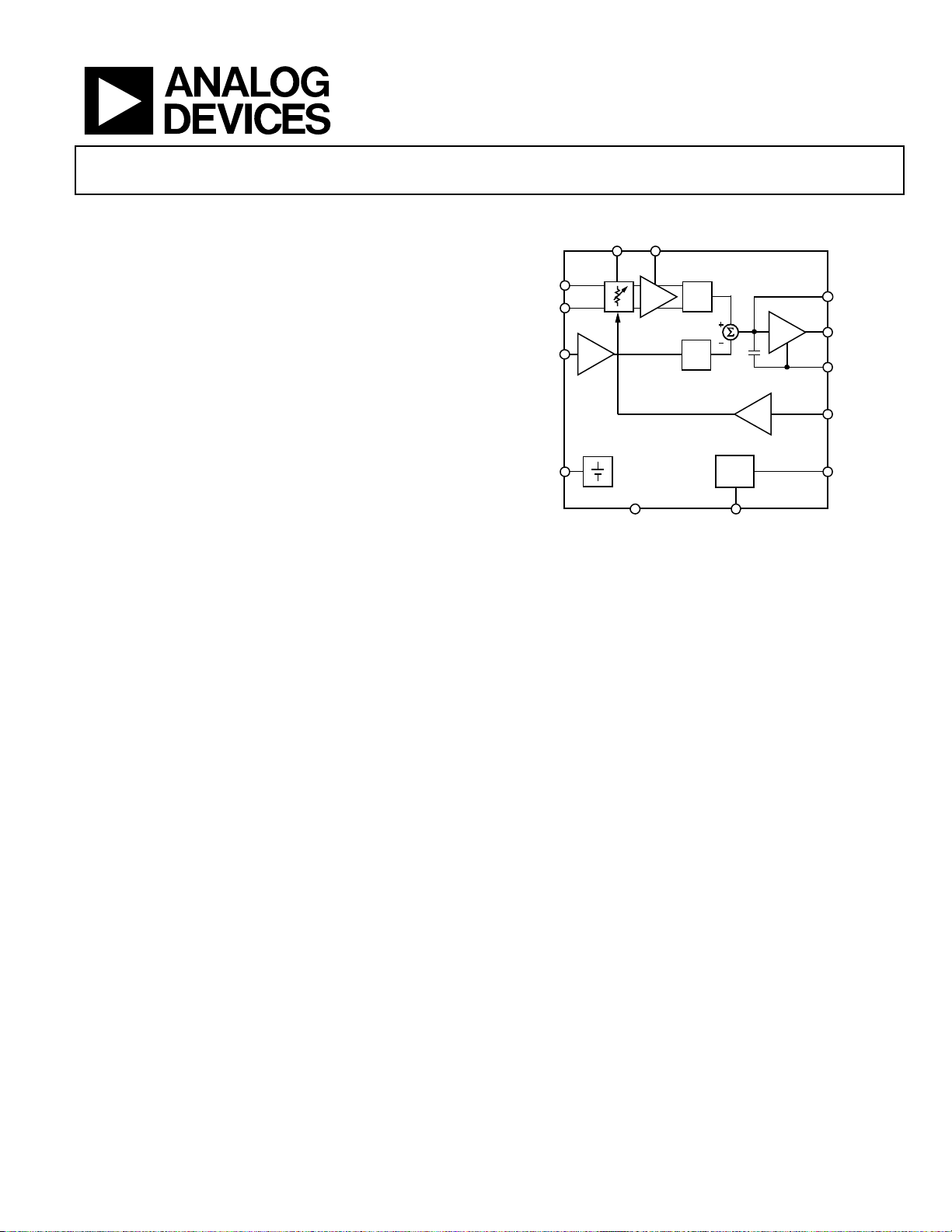
65 dB TruPwr™ Detector
AD8362
FUNCTIONAL BLOCK DIAGRAM
CHPF
DECL
INHI
INLO
TGT
AD8362
REF
amplifier, thus balancing the setpoint against the input power.
Optionally, the voltage at VSET can be a replica of the RF signal’s
amplitude modulation, in which case the overall effect is to
remove the modulation component prior to detection and lowpass filtering. The corner frequency of the averaging filter can
be lowered without limit by adding an external capacitor at the
CLPF pin. The AD8362 can be used to determine the true power
of a high frequency signal having a complex low frequency
modulation envelope, or simply as a low frequency rms voltmeter. The high-pass corner generated by its offset-nulling
loop can be lowered by a capacitor added on the CHPF pin.
Used as a power measurement device, VOUT is strapped to
VSET. The output is then proportional to the logarithm of the
rms value of the input. In other words, the reading is presented
directly in decibels and is conveniently scaled 1 V per decade,
or 50 mV/dB; other slopes are easily arranged. In controller
modes, the voltage applied to VSET determines the power level
required at the input to null the deviation from the setpoint.
The output buffer can provide high load currents.
The AD8362 has 1.3 mW power consumption when powered
down by a logic high applied to the PWDN pin. It powers up
within about 20 µs to its nominal operating current of 20 mA at
25°C. The AD8362 is supplied in a 16-lead TSSOP for operation
over the temperature range of −40°C to +85°C.
2
x
2
x
Figure 1.
BIAS
PWDNCOMM
CLPF
VOUT
ACOM
VSET
VPOS
02923-001
Rev. D
Information furnished by Analog Devices is believed to be accurate and reliable. However, no
responsibility is assumed by Anal og Devices for its use, nor for any infringements of patents or ot her
rights of third parties that may result from its use. Specifications subject to change without notice. No
license is granted by implication or otherwise under any patent or patent rights of Analog Devices.
Trademarks and registered trademarks are the property of their respective owners.
One Technology Way, P.O. Box 9106, Norwood, MA 02062-9106, U.S.A.
Tel: 781.329.4700 www.analog.com
Fax: 781.461.3113 ©2003–2007 Analog Devices, Inc. All rights reserved.

AD8362
TABLE OF CONTENTS
Features.............................................................................................. 1
Applications....................................................................................... 1
Functional Block Diagram .............................................................. 1
General Description ......................................................................... 1
Revision History ............................................................................... 2
Specifications..................................................................................... 3
Absolute Maximum Ratings............................................................ 6
ESD Caution.................................................................................. 6
Pin Configuration and Function Descriptions............................. 7
Equivalent Circuits........................................................................... 8
Typical Performance Characteristics ............................................. 9
Characterization Setup .................................................................. 15
Equipment................................................................................... 15
Analysis........................................................................................ 15
Circuit Description......................................................................... 16
Square Law Detection................................................................ 16
Voltage vs. Power Calibration................................................... 17
Offset Elimination...................................................................... 18
Time-Domain Response of the Closed Loop .........................18
REVISION HISTORY
6/07—Rev. C to Rev. D
Changes to Features, General Description.................................... 1
Changes to Table 1............................................................................ 3
Changes to Table 2............................................................................ 6
Added Figure 21 to Figure 25........................................................ 11
Changes to Equipment Section..................................................... 15
Changes to Circuit Description Section...................................... 16
Changes to Single-Ended Input Drive Section ........................... 19
Changes to Choosing a Value for CHPF section........................ 21
Changes to Choosing a Value for CLPF section......................... 21
Changes to Figure 57...................................................................... 23
Changes to Figure 58...................................................................... 24
Added Temperature Compensation at Various WiMAX
Frequencies up to 3.8 GHz Section.............................................. 24
Changes to Ordering Guide.......................................................... 31
9/05—Rev. B to Rev. C
Changes to Specifications................................................................ 3
Changes to Table 3 ........................................................................... 7
Deleted Figure 16 to Figure 18; Renumbered Sequentially ......10
Changes to Figure 32 and Figure 33 ............................................ 13
Operation in RF Measurement Mode.......................................... 19
Basic Connections...................................................................... 19
Device Disable ............................................................................ 19
Recommended Input Coupling................................................ 19
Operation at Low Frequencies.................................................. 20
Choosing a Value for CHPF...................................................... 21
Choosing a Value for CLPF....................................................... 21
Adjusting VTGT to Accommodate Signals with Very High
Crest Factors ............................................................................... 22
Altering the Slope....................................................................... 22
Temperature Compensation and Reduction of Transfer
Function Ripple.......................................................................... 23
Temperature Compensation at Various WiMAX Frequencies up
to 3.8 GHz........................................................................................ 24
Operation in Controller Mode................................................. 26
RMS Voltmeter with 90 dB Dynamic Range.......................... 27
AD8362 Evaluation Board ............................................................ 28
Outline Dimensions....................................................................... 31
Ordering Guide .......................................................................... 31
Replaced Circuit Description Section ......................................... 15
Changes to Operation in RF Measurement Mode Section ...... 18
Deleted Using the AD8362 Section ............................................. 20
Deleted Main Modes of Operation Section ................................ 22
Changes to Operation in Controller Mode Section .................. 23
Changes to AD8362 Evaluation Board Section.......................... 25
Deleted General Applications Section......................................... 29
3/04—Rev. A to Rev. B
Updated Format .................................................................Universal
Changes to Specifications.................................................................3
Changes to the Offset Elimination Section................................. 16
Changes to the Operation at Low Frequencies Section ............ 17
Changes to the Time-Domain Response of the Closed
Loop Section.................................................................................... 17
Changes to Equation 13................................................................. 24
Changes to Table 5......................................................................... 31
6/03—Rev. 0 to Rev. A
Updated Ordering Guide .................................................................5
Change to Analysis Section........................................................... 12
Updated AD8362 Evaluation Board Section .............................. 26
2/03—Revision 0: Initial Version
Rev. D | Page 2 of 32

AD8362
SPECIFICATIONS
VS = 5 V, T = 25°C, ZO = 50 Ω, differential input drive via balun1, VTGT connected to VREF, VOUT tied to VSET, unless otherwise noted.
Table 1.
Parameter Conditions Min Typ Max Unit
OVERALL FUNCTION
Maximum Input Frequency 3.8 GHz
Input Power Range (Differential)
Nominal Low End of Range −52 dBm
Nominal High End of Range 8 dBm
Input Voltage Range (Differential) RMS voltage at input terminals, f ≤ 2.7 GHz, into input of the device
Nominal Low End of Range 1.12 mV rms
Nominal High End of Range 1.12 V rms
Input Power Range (S-Sided) Single-ended drive, CW input, f ≤ 2.7 GHz, into input resistive network2
Nominal Low End of Range −40 dBm
Nominal High End of Range 0 dBm
Input Voltage Range (S-Sided) RMS voltage at input terminals, f ≤ 2.7 GHz
Nominal Low End of Range 2.23 mV rms
Nominal High End of Range 2.23 V rms
Input Power Range (S-Sided) Single-ended drive, CW input, f ≥ 2.7 GHz, into matched input network3
Nominal Low End of Range −35 dBm
Nominal High End of Range 12
Output Voltage Range RL ≥ 200 Ω to ground
Nominal Low End of Range 100 mV
Nominal High End of Range In general, VS − 0.1 V 4.9 V
Output Scaling (Log Slope) 50 mV/dB
Law Conformance Error Over central 60 dB range, f ≤ 2.7 GHz ±0.5 dB
RF INPUT INTERFACE Pin INHI, Pin INLO, ac-coupled, at low frequencies
Input Resistance Single-ended drive, with respect to DECL 100 Ω
Differential drive 200 Ω
OUTPUT INTERFACE Pin VOUT
Available Output Range RL ≥ 200 Ω to ground 0.1 4.9 V
Absolute Voltage Range
Nominal Low End of Range Measurement mode, f = 900 MHz, PIN = −52 dBm 0.32 0.48 V
Nominal High End of Range Measurement mode, f = 900 MHz, PIN = +8 dBm 3.44 3.52 V
Source/Sink Current VOUT held at VS/2, to 1% change 48 mA
Slew Rate Rising CL = open 60 V/μs
Slew Rate Falling CL = open 5 V/μs
Rise Time, 10% to 90% 0.2 V to 1.8 V, CLPF = Open 45 ns
Fall Time, 90% to 10% 1.8 V to 0.2 V, CLPF = Open 0.4 μs
Wideband Noise CLPF = 1000 pF, f
VSET INTERFACE Pin VSET
Nominal Input Voltage Range To ±1 dB error 0.5 3.75 V
Input Resistance 68 kΩ
Scaling (Log Slope) f = 900 MHz 46 50 54 mV/dB
Scaling (Log Intercept) f = 900 MHz, into 1:4 balun −64 −60 −56 dBm
−77 −73 −69 dBV
VOLTAGE REFERENCE Pin VREF
Output Voltage 25°C 1.225 1.25 1.275 V
Temperature Sensitivity −40°C ≤ TA ≤ +85°C 0.08 mV/°C
Output Resistance 8 Ω
dB referred to 50 Ω impedance level, f ≤ 2.7 GHz, into 1:4 balun
≤ 100 kHz 70 nV/√Hz
SPOT
1
4
dBm
Rev. D | Page 3 of 32

AD8362
Parameter Conditions Min Typ Max Unit
RMS TARGET INTERFACE Pin VTGT
Nominal Input Voltage Range Measurement range = 60 dB, to ±1 dB error 0.625 2.5 V
Input Bias Current VTGT = 1.25 V −28 μA
VTGT = 0 V −52 μA
Incremental Input Resistance 52 kΩ
POWER-DOWN INTERFACE Pin PWDN
Logic Level to Enable Logic low enables 1 V
Logic Level to Disable Logic high disables 3 V
Input Current Logic high 230 μA
Logic low 5 μA
Enable Time From PWDN low to VOUT within 10% of final value, CLPF = 1000 pF 14.5 ns
Disable Time From PWDN high to VOUT within 10% of final value, CLPF = 1000 pF 2.5 μs
POWER SUPPLY INTERFACE Pin VPOS
Supply Voltage 4.5 5 5.5 V
Quiescent Current 20 22 mA
Supply Current When disabled 0.2 mA
900 MHz
Dynamic Range Error referred to best-fit line (linear regression)
±1.0 dB linearity, CW input 65 dB
±0.5 dB linearity, CW input 62 dB
Deviation vs. Temperature Deviation from output at 25°C
−40°C < TA < +85°C, PIN = −45 dBm −1.7 dB
−40°C < TA < +85°C, PIN = −20 dBm −1.4 dB
−40°C < TA < +85°C, PIN = +5 dBm −1.0 dB
Logarithmic Slope 46 50 54 mV/dB
Logarithmic Intercept −64 −60 −56 dBm
Deviation from CW Response 5.5 dB peak-to-rms ratio (IS95 reverse link) 0.2 dB
12.0 dB peak-to-rms ratio (W-CDMA 4 channels) 0.2 dB
18.0 dB peak-to-rms ratio (W-CDMA 15 channels) 0.5 dB
1.9 GHz
Dynamic Range Error referred to best-fit line (linear regression)
±1 dB linearity, CW input 65 dB
±0.5 dB linearity, CW input 62 dB
Deviation vs. Temperature Deviation from output at 25°C
−40°C < TA < +85°C, PIN = −45 dBm −0.6 dB
−40°C < TA < +85°C, PIN = −20 dBm −0.5 dB
−40°C < TA < +85°C, PIN = +5 dBm −0.3 dB
Logarithmic Slope 51 mV/dB
Logarithmic Intercept −59 dBm
Deviation from CW Response 5.5 dB peak-to-rms ratio (IS95 reverse link) 0.2 dB
12.0 dB peak-to-rms ratio (W-CDMA 4 channels) 0.2 dB
18.0 dB peak-to-rms ratio (W-CDMA 15 channels) 0.5 dB
2.2 GHz
Dynamic Range Error referred to best-fit line (linear regression)
±1.0 dB linearity, CW input 65 dB
±0.5 dB linearity, CW input 65 dB
Deviation vs. Temperature Deviation from output at 25°C
−40°C < TA < +85°C, PIN = −45 dBm −1.8 dB
−40°C < TA < +85°C, PIN = −20 dBm −1.6 dB
−40°C < TA < +85°C, PIN = +5 dBm −1.3 dB
Logarithmic Slope 50.5 mV/dB
Logarithmic Intercept −61 dBm
Deviation from CW Response 5.5 dB peak-to-rms ratio (IS95 reverse link) 0.2 dB
12.0 dB peak-to-rms ratio (W-CDMA 4 channels) 0.2 dB
18.0 dB peak-to-rms ratio (W-CDMA 15 channels) 0.5 dB
Rev. D | Page 4 of 32

AD8362
Parameter Conditions Min Typ Max Unit
2.7 GHz
Dynamic Range Error referred to best-fit line (linear regression)
±1.0 dB linearity, CW input 63 dB
±0.5 dB linearity, CW input 62 dB
Deviation vs. Temperature Deviation from output at 25°C
−40°C < TA < +85°C, PIN = −40 dBm −5.3 dB
−40°C < TA < +85°C, PIN = −15 dBm −5.5 dB
−40°C < TA < +85°C, PIN = +5 dBm −4.8 dB
Logarithmic Slope 50.5 mV/dB
Logarithmic Intercept −58 dBm
Deviation from CW Response 5.5 dB peak-to-rms ratio (IS95 reverse link) 0.2 dB
12.0 dB peak-to-rms ratio (W-CDMA 4 channels) 0.2 dB
18.0 dB peak-to-rms ratio (W-CDMA 15 channels) 0.4 dB
3.65 GHz
Single-ended drive
Dynamic Range Error referred to best-fit line (linear regression)
±1.0 dB linearity, CW input 51 dB
±0.5 dB linearity, CW input 50 dB
Deviation vs. Temperature Deviation from output at 25°C
−40°C < TA < +85°C, PIN = −35 dBm −3 dB
−40°C < TA < +85°C, PIN = −15 dBm −3.5 dB
−40°C < TA < +85°C, PIN = +10 dBm −3.5 dB
Logarithmic Slope 51.7 mV/dB
Logarithmic Intercept −45 dBm
1
1:4 balun transformer, M/A-COM ETC 1.6-4-2-3.
2
See Figure 48.
3
See Figure 50.
4
The limitation of the high end of the power range is due to the test equipment not the device under test.
3
Rev. D | Page 5 of 32
AD8362
ABSOLUTE MAXIMUM RATINGS
Table 2.
Parameter Rating
Supply Voltage VPOS 5.5 V
Input Power (Into Input of Device) 15 dBm
Equivalent Voltage 2 V rms
Internal Power Dissipation 500 mW
θJA 125°C/W
Maximum Junction Temperature 125°C
Operating Temperature Range −40°C to +85°C
Storage Temperature Range −65°C to +150°C
Lead Temperature (Soldering, 60 sec) 300°C
Stresses above those listed under Absolute Maximum Ratings
may cause permanent damage to the device. This is a stress
rating only; functional operation of the device at these or any
other conditions above those indicated in the operational
section of this specification is not implied. Exposure to absolute
maximum rating conditions for extended periods may affect
device reliability.
ESD CAUTION
Rev. D | Page 6 of 32
AD8362
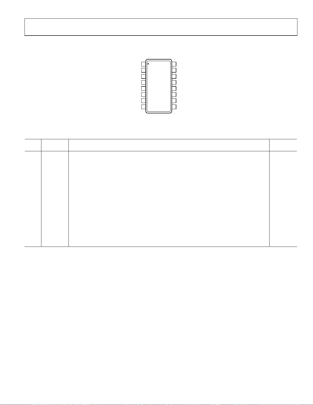
PIN CONFIGURATION AND FUNCTION DESCRIPTIONS
1
COMM
2
CHPF
3
DECL
INHI
INLO
DECL
PWDN
COMM CLPF
AD8362
TOP VIEW
4
(Not to Scale)
5
6
7
8
16
ACOM
15
VREF
14
VTGT
13
VPOS
12
VOUT
11
VSET
10
ACOM
9
02923-002
Figure 2. Pin Configuration
Table 3. Pin Function Descriptions
Pin
No.
Mnemonic Description
Equivalent
Circuit
1, 8 COMM Common Connection. Connect via low impedance to system common.
2 CHPF Input HPF. Connect to common via a capacitor to determine 3 dB point of input signal high-pass filter.
3, 6 DECL
Decoupling Terminals for INHI and INLO. Connect to common via a large capacitance to complete
input circuit.
4, 5 INHI , INLO
Differential Signal Input Terminals. Input Impedance = 200 Ω. Can also be driven single-ended, in
Circuit A
which case, the input impedance reduces to 100 Ω.
7 PWDN Disable/Enable Control Input. Apply logic high voltage to shut down the AD8362.
9 CLPF Connection for Ground Referenced Loop Filter Integration (Averaging) Capacitor.
10, 16 ACOM Analog Common Connection for Output Amplifier.
11 VSET
Setpoint Input. Connect directly to VOUT for measurement mode. Apply setpoint input to this pin for
Circuit B
controller mode.
12 VOUT RMS Output. In measurement mode, VOUT is normally connected directly to VSET. Circuit C
13 VPOS Connect to 5 V Power Supply.
14 VTGT
The logarithmic intercept voltage is proportional to the voltage applied to this pin. The use of a lower
Circuit D
target voltage increases the crest factor capacity. Normally connected to VREF.
15 VREF General-Purpose Reference Voltage Output of 1.25 V. Usually connected only to VTGT. Circuit E
Rev. D | Page 7 of 32
AD8362
EQUIVALENT CIRCUITS
DECL
INHI
INLO
DECL
COMM
100Ω
100Ω
VPOS
Figure 3. Circuit A
VGA
VPOS
COMM
VPOS
VSET
ACOM
COMM
~35kΩ
~35kΩ
VSET
INTERFACE
CLPF
02923-004
Figure 4. Circuit B
VPOS
50kΩ
VTGT
ACOM
02923-003
COMM
50kΩ
VTGT
INTERF ACE
GAIN = 0.12
02923-005
~0.35V
Figure 5. Circuit C
RAIL-TO-RAIL
0.7V
Figure 6. Circuit D
SOURCE ONLY
REF BUF
13kΩ
Figure 7. Circuit E
OUTPUT
2kΩ
500Ω
5kΩ
VPOS
VOUT
ACOM
COMM
VPOS
VOUT
ACOM
COMM
02923-006
02923-007
Rev. D | Page 8 of 32
AD8362
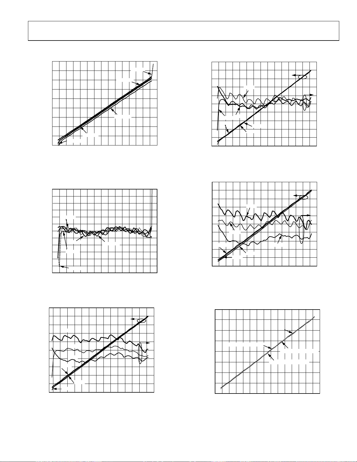
TYPICAL PERFORMANCE CHARACTERISTICS
4.5
2200MHz
2700MHz
–10
100MHz
15
02923-008
4.0
3.5
3.0
2.5
2.0
VOUT (V)
1.5
1.0
0.5
0
–55 –50 –45 –40 –35 –30 –25 –20 –15 –5 0 5 10
–60
900MHz
1900MHz
INPUT AMPLI TUDE (dBm)
Figure 8. Output Voltage (VOUT) vs. Input Amplitude (dBm),
Frequencies: 100 MHz, 900 MHz, 1900 MHz, 2200 MHz, and 2700 MHz;
Sine Wave, Differential Drive
3.0
2.5
2.0
1.5
100MHz
1.0
0.5
0
–0.5
–1.0
ERROR IN VOUT (dB)
–1.5
–2.0
–2.5
–3.0
–60
2200MHz
900MHz
2700MHz
–55 –50 –45 –40 –35 –30 –25 –20 –15 –5 0 5 10
INPUT AMPLI TUDE (dBm)
1900MHz
–10
15
02923-009
Figure 9. Logarithmic Law Conformance vs. Input Amplitude,
Frequencies: 100 MHz, 900 MHz, 1900 MHz, 2200 MHz, and 2700 MHz;
Sine Wave, Differential Drive
4.0
3.6
3.2
2.8
2.4
2.0
VOUT (V)
1.6
1.2
0.8
0.4
–40°C
+25°C
+85°C
–40°C
+85°C
+25°C
0
–50 –45 –40 –35 –30 –25 –20 –15 –5 0 5 10
–55
INPUT AMPLI TUDE (dBm)
–10
3.0
2.4
1.8
1.2
0.6
0
–0.6
–1.2
–1.8
–2.4
–3.0
15
Figure 10. VOUT and Law Conformance vs. Input Amplitude,
Frequency 900 MHz, Sine Wave, Temperatures: −40°C, +25°C, and +85°C
ERROR IN VOUT (dB)
02923-010
4.0
3.6
3.2
2.8
2.4
2.0
VOUT (V)
1.6
+25°C
1.2
–40°C
0.8
0.4
0
–60 –55 –50 –45 –40 –35 –30 –25 –20 –15 –5 0 5 10 15–10
–40°C
+85°C
+25°C
+85°C
INPUT AMPLI TUDE (dBm)
3.0
2.4
1.8
1.2
0.6
0
–0.6
–1.2
–1.8
–2.4
–3.0
ERROR IN VOUT (dB)
02923-011
Figure 11. VOUT and Law Conformance vs. Input Amplitude,
Frequency 1900 MHz, Sine Wave, Temperatures: −40°C, +25°C, and +85°C
VOUT (V)
4.0
3.6
3.2
2.8
2.4
2.0
1.6
1.2
–40°C
0.8
0.4
0
–50 –45 –40 –35 –30 –25 –20 –15 –5 0 5 10
–60
–55
–40°C
+25°C
+85°C
+25°C
INPUT AMPLITUDE (dBm)
+85°C
–10
3.0
2.4
1.8
1.2
0.6
0
–0.6
–1.2
ERROR IN VOUT (dB)
–1.8
–2.4
–3.0
15
02923-012
Figure 12. VOUT and Law Conformance vs. Input Amplitude,
Frequency 2200 MHz, Sine Wave, Temperatures: −40°C, +25°C, and +85°C
4.0
3.5
3.0
2.5
2.0
VOUT (V)
1.5
1.0
0.5
0
–60
IS95 REVERSE LINK
–55 –50 –45 –40 –35 –30 –25 –20 –15 –5 0 5 10
INPUT AMPLI TUDE (dBm)
CW
W-CDMA 8-CHANNEL
W-CDMA 15-CHANNEL
–10
15
02923-013
Figure 13. VOUT vs. Input Amplitude with Different Waveforms, CW, IS95
Reve rse Link, W-C DMA 8-Chann el, W-CDMA 1 5-Channel, Frequency 900 MHz
Rev. D | Page 9 of 32
AD8362
3.0
2.5
2.0
1.5
W-CDMA 8-CHANNEL
–10
ERROR IN VOUT (d B)
1.0
0.5
–0.5
–1.0
–1.5
–2.0
–2.5
–3.0
0
–60
IS95 REVERSE LINK
CW
W-CDMA 15-CHANNEL
–55 –50 –45 –40 –35 –30 –25 –20 –15 –5 0 5 10
INPUT AMPLITUDE (dBm)
Figure 14. Output Error from CW Linear Reference vs. Input Amplitude
with Different Waveforms, CW, IS95 Reverse Link, W-CDMA 8-Channel,
W-CDMA 15-Channel, Frequency 900 MHz, V
3.0
2.5
2.0
1.5
1.0
0.5
0
–0.5
–1.0
ERROR IN VOUT ( dB)
–1.5
–2.0
–2.5
–3.0
–55 –50 –45 –40 –35 –30 –25 –20 –15 –5 0 5 10–10
W-CDMA
4-CHANNEL
CW
W-CDMA 15-CHANNEL
INPUT AMPLITUDE (dBm)
8-CHANNEL
W-CDMA
= 1.25 V
TGT
4.0
3.5
3.0
2.5
2.0
VOUT (V)
1.5
1.0
0.5
0
15
02923-014
–55 –50 –45 –40 –35 –30 –25 –20 –15 –5 0 5
INPUT AMPLI TUDE (dBm)
–10
10
02923-017
Figure 17. VOUT vs. Input Amplitude, 3 Sigma to Either Side of Mean,
Sine Wave, Frequency 1900 MHz, Part-to-Part Variation
3.0
2.5
2.0
1.5
1.0
0.5
0
–0.5
–1.0
ERROR IN VOUT (dB)
–1.5
–2.0
–2.5
–3.0
–50 –45 –40 –35 –30 –25 –20 –15 –5 0 5 10
–55
02923-015
–40°C
+25°C
INPUT AMPLITUDE (dBm)
+85°C
–10
02923-018
Figure 15. Output Error from CW Linear Reference vs. Input Amplitude
with Different W-CDMA Channel Loading, 4-Channel, 8-Channel,
15-Channel, Frequency 2200 MHz, V
4.0
3.5
3.0
2.5
2.0
VOUT (V)
1.5
1.0
0.5
0
–55 –50 –45 –40 –35 –30 –25 –20 –15 –5 0 5 10
INPUT AMPLI TUDE (dBm)
–10
= 1.25 V
TGT
Figure 16. VOUT vs. Input Amplitude, 3 Sigma to Either Side of Mean,
Sine Wave, Frequency 900 MHz, Part-to-Part Variation
02923-016
Rev. D | Page 10 of 32
Figure 18. Logarithmic Law Conformance vs. Input Amplitude,
3 Sigma to Either Side of Mean, Sine Wave, Frequency 900 MHz,
Temperatures: −40°C, +25°C, and +85°C
3.0
2.5
2.0
1.5
1.0
0.5
0
–0.5
–1.0
ERROR IN VOUT (dB)
–1.5
–2.0
–2.5
–3.0
–50 –45 –40 –35 –30 –25 –20 –15 –5 0 5 10
–55
–45°C
+85°C
INPUT AMPLITUDE (dBm)
+25°C
–10
Figure 19. Logarithmic Law Conformance vs. Input Amplitude,
3 Sigma to Either Side of Mean, Sine Wave, Frequency 1900 MHz,
Temperatures: −40°C, +25°C, and +85°C
02923-019

AD8362
3.0
2.5
2.0
1.5
1.0
0.5
0
–0.5
–1.0
ERROR IN VOUT (dB)
–1.5
–2.0
–2.5
–3.0
–50 –45 –40 –35 –30 –25 –20 –15 –5 0 5 10
–55
–40°C
+85°C
+25°C
INPUT AMPLITUDE (dBm)
–10
4.0
+85°C
+25°C
–40°C
3.5
3.0
2.5
2.0
VOUT (V)
1.5
1.0
0.5
0
–60 20
–50 –40 –30 –20 –10 0 10
02923-020
INPUT AMPLITUDE (dBm)
8
6
4
2
0
ERROR (dB)
–2
–4
–6
–8
02923-023
Figure 20. Logarithmic Law Conformance vs. Input Amplitude,
3 Sigma to Either Side of Mean, Sine Wave, Frequency 2200 MHz,
Temperatures: −40°C, +25°C, and +85°C
4.0
+85°C
+25°C
–40°C
3.5
3.0
2.5
2.0
VOUT (V)
1.5
1.0
0.5
0
–60 20
–50 –40 –30 –20 –10 0 10
INPUT AMPLITUDE (dBm)
8
6
4
2
0
ERROR (dB)
–2
–4
–6
–8
Figure 21. VOUT and Law Conformance vs. Input Amplitude for 15 Devices,
Frequency 2350 MHz, Sine Wave, Temperatures: −40°C, +25°C, and +85°C,
No Temperature Compensation, Single-Ended Drive, See
4.0
+85°C
+25°C
–40°C
3.5
3.0
Figure 50
8
6
4
Figure 23. VOUT and Law Conformance vs. Input Amplitude for 15 Devices,
Frequency 2800 MHz, Sine Wave, Temperatures: −40°C, +25°C, and +85°C,
No Temperature Compensation, Single-Ended Drive, See
4.0
3.5
3.0
2.5
2.0
VOUT (V)
1.5
1.0
0.5
0
–60 20
–50 –40 –30 –20 –10 0 10
02923-021
INPUT AMPLI TUDE (dBm)
Figure 50
+85°C
+25°C
–40°C
8
6
4
2
0
ERROR (dB)
–2
–4
–6
–8
02923-024
Figure 24. VOUT and Law Conformance vs. Input Amplitude for 15 Devices,
Frequency 3450 MHz, Sine Wave, Temperatures: −40°C, +25°C, and +85°C,
No Temperature Compensation, Single-Ended Drive, See
4.0
3.5
3.0
Figure 50
8
6
4
2.5
2.0
VOUT (V)
1.5
1.0
0.5
0
–50 –40 –30 –20 –10 0 10
–60 20
INPUT AMPLITUDE (dBm)
2
0
ERROR (dB)
–2
–4
–6
–8
Figure 22. VOUT and Law Conformance vs. Input Amplitude for 15 Devices,
Frequency 2600 MHz, Sine Wave, Temperatures: −40°C, +25°C, and +85°C,
No Temperature Compensation, Single-Ended Drive, See
Figure 50
Rev. D | Page 11 of 32
2.5
2.0
VOUT (V)
1.5
1.0
0.5
0
–60 20
–50 –40 –30 –20 –10 0 10
02923-022
INPUT AMPLITUDE (dBm)
2
0
ERROR (dB)
–2
–4
–6
–8
2923-025
Figure 25. VOUT and Law Conformance vs. Input Amplitude for 15 Devices,
Frequency 3650 MHz, Sine Wave, Temperatures: −40°C, +25°C, and +85°C,
No Temperature Compensation, Single-Ended Drive, See
Figure 50

AD8362
–
52.0
2.0
51.5
51.0
50.5
SLOPE (mV)
50.0
49.5
49.0
900
1000
1100
1200
1300
1400
1500
1600
1700
FREQUENCY (MHz)
1800
Figure 26. Logarithmic Slope vs. Frequency,
Temperatures: −40°C, +25°C, and +85°C
53
–54
–55
–56
–57
–58
–59
INTERCEPT (dBm)
–60
–61
–62
–63
900
1000
1100
1200
1300
1400
1500
1600
1700
FREQUENCY (MHz)
1800
Figure 27. Logarithmic Intercept vs. Frequency,
Temperatures: −40°C, +25°C, and +85°C
1900
1900
2000
2000
2100
2100
2200
2200
+85°C
+25°C
–40°C
2300
2300
2400
+85°C
+25°C
2400
2500
–40°C
2500
2600
2600
2700
2700
1.5
1.0
1900MHz
0.5
0
–0.5
–1.0
CHANGE IN INTERCEPT (dB)
–1.5
2200MHz
–2.0
–40
02923-026
900MHz
–30 –20 –10 0 10 20 30 40 50 70 80 90
TEMPERATURE ( °C)
60
02923-029
Figure 29. Change in Logarithmic Intercept vs. Temperature, 3 Sigma to
Either Side of Mean, Frequencies: 900 MHz, 1900 MHz, and 2200 MHz
100
80
60
HITS
40
20
0
48 5349 50 51 52
02923-027
SLOPE (mV/dB)
2923-030
Figure 30. Slope Distribution, Frequency 900 MHz
3.0
2.5
2.0
CHANGE IN SLOPE (mV)
–0.5
–1.0
–1.5
–2.0
–2.5
–3.0
1.5
1.0
0.5
0
–40
1900MHz
2200MHz
–30 –20 –10 0 10 20 30 40 50 70 80 90
TEMPERATURE ( °C)
900MHz
60
02923-028
Figure 28. Change in Logarithmic Slope vs. Temperature, 3 Sigma to Either
80
70
60
50
40
HITS
30
20
10
0
–61.0 –58.0–60.5 –60.0 –59.5 –59.0 –58.5
INTERCEPT (dBm)
Figure 31. Logarithmic Intercept Distribution, Frequency 900 MHz
02923-031
Side of Mean, Frequencies: 900 MHz, 1900 MHz, and 2200 MHz
Rev. D | Page 12 of 32

AD8362
5.0
4.5
4.0
3.5
3.0
2.5
VOUT (V)
2.0
1.5
1.0
0.5
RF BURST
ENABLE
+2dBm
VO
UT
0.5V/DIV
0
210142
0
46
–10dBm
–20dBm
–30dBm
812 1816
TIME (µs)
2V/DIV
6
4
2
0
–2
–4
–6
–8
RF BURST ENABLE (V)
–10
–12
–14
0
2923-032
5.0
4.5
4.0
3.5
3.0
2.5
VOUT (V)
2.0
1.5
0.5V/DIV
1.0
0.5
0
0
210142
46
+2dBm
–10dBm
–20dBm
–30dBm
812 1816
TIME (ms)
6
4
2V/DIV
2
0
–2
–4
–6
–8
POWER-DOW N PIN (V)
–10
–12
–14
0
02923-035
Figure 32. Output Response to RF Burst Input for Various
RF Input Levels, Carrier Frequency 900 MHz, CLPF = Open
5.0
4.5
RF BURST
4.0
3.5
3.0
2.5
VOUT (V)
2.0
1.5
1.0
0.5
ENABLE
+2dBm
–10dBm
VO
UT
0.5V/DIV
0
0
210142
46
–20dBm
–30dBm
812 1816
TIME (ms)
2V/DIV
6
4
2
0
–2
–4
–6
–8
RF BURST ENABLE (V)
–10
–12
–14
0
Figure 33. Output Response to RF Burst Input for Various RF Input Levels,
Carrier Frequency 900 MHz, CLPF = 0.1 µF
5.0
4.5
PO
W
ER-
DO
W
4.0
3.5
3.0
2.5
VOUT (V)
2.0
1.5
1.0
0.5
N
PIN
VO
UT
0.5V/DIV
0
210142
0
46
+2dBm
–10dBm
–20dBm
–30dBm
812 1816
TIME (µs)
6
4
2V/DIV
2
0
–2
–4
–6
–8
POWER-DOW N PIN (V)
–10
–12
–14
0
Figure 34. Output Response Using Power-Down Mode for Various RF Input
Levels, Carrier Frequency 900 MHz, CLPF = 0
Figure 35. Output Response Using Power-Down Mode for Various RF Input
Levels, Carrier Frequency 900 MHz, CLPF = 0.1 µF
5.5
5.0
4.5
4.0
3.5
3.0
VOUT (V)
2.5
2.0
1.5
1.0
02923-033
1V/D
0
0
210142
IV
46
VPOS
812 1816
TIME (ms)
2V/DIV
+2dBm
–10dBm
–20dBm
–30dBm
6
4
2
0
–2
–4
–6
–8
POWER-DOW N PIN (V)
–10
–12
–14
0
2923-036
Figure 36. Output Response to Gating on Power Supply for Various RF Input
Levels, Carrier Frequency 900 MHz, CLPF = 0
100MHz
3GHz
2923-034
02923-037
Figure 37. INHI, INLO Differential Input Impedance, 100 MHz to 3 GHz
Rev. D | Page 13 of 32

AD8362
5
0
–5
300
250
–10
–15
CHANGE IN VREF (mV)
–20
–25
–30
–30–20–100 1020304050 708090
–40
TEMPERATURE ( °C)
60
Figure 38. Change in VREF vs. Temperature, 3 Sigma to Either Side of Mean
200
HITS
150
100
50
0
2923-038
1.230 1.2701.235 1.240 1.245 1.250 1.2601.255 1.265
VREF (V)
02923-039
Figure 39. VREF Distribution
Rev. D | Page 14 of 32

AD8362
(
)
CHARACTERIZATION SETUP
EQUIPMENT
The general hardware configuration used for most of the AD8362
characterization is shown in
Figure 40. The signal source is a
Rohde & Schwarz SMIQ03B. A 1:4 balun transformer is used to
transform the single-ended RF signal to differential form. For
frequencies above 3.0 GHz, an Agilent 8521A signal source
was used. For the response measurements in
Figure 32 and
Figure 33, the configuration shown in Figure 41 is used. For
Figure 34 and Figure 35, the configuration shown in Figure 42
is used. For
Figure 36, the configuration shown in Figure 43 is
used.
AD8362
CHARACTERIZATION
SMIQ03B
RF SOURCE
PC
CONTROLL ER
3dB
RFIN
Figure 40. Primary Characterization Setup
BOARD
VOUT
MULTIMETER
HP34401A
ANALYSIS
The slope and intercept are derived using the coefficients of
a linear regression performed on data collected in its central
operating range. Error is stated in two forms: error from the
linear response to the CW waveform and output delta from
25°C performance.
The error from linear response to the CW waveform is the
decibel difference in output from the ideal output defined by
the conversion gain and output reference. This is a measure of
the linearity of the device response to both CW and modulated
waveforms. The error in dB is calculated by
PPSlopeVOUT
−×−
IN
()
Error
where P
Z
=dB
Slope
is the x intercept, expressed in dBm.
Error from the linear response to the CW waveform is not a
measure of absolute accuracy because it is calculated using
the slope and intercept of each device. However, it verifies the
linearity and the effect of modulation on the device response.
Error from the 25°C performance uses the performance of a
given device and waveform type as the reference; it is predominantly a measurement of output variation with temperature.
Z
(1)
2923-040
TEK TDS5104
SCOPE
SMT03
SIGNAL
GENERATO R
RF 50Ω
TEK P5050
VOLTAGE PROBE
BALUN
3dB
C2
AD8362
ACOM
COMM
VREF
CHPF
C1
C3
DECL
INHI
INLO
DECL
PWDN
COMM
VTGT
VPOS
VOUT
VSET
ACOM
CLPF
Figure 41. Response Measurement Setup for Modulated Pulse
TEK TDS5104
SCOPE
SMT03
SIGNAL
GENERATOR
RF 50Ω
HP8112A
PULSE
GENERATO R
TEK P5050
VOLTAGE PROBE
BALUN
3dB
C2
AD8362
COMM
ACOM
CHPF
DECL
INHI
INLO
DECL
PWDN
COMM
VREF
VTGT
VPOS
VOUT
VSET
ACOM
CLPF
C1
C3
Figure 42. Response Measurement Setup for Power-Down Step
BALUN
3dB
SMT03
SIGNAL
GENERATOR
RF 50Ω
AD811
732Ω
AD8362
COMM
ACOM
CHPF
C1
DECL
INHI
INLO
C2
DECL
C3
PWDN
COMM
VREF
VTGT
VPOS
VOUT
VSET
ACOM
CLPF
0.01µF 100pF
50Ω
C4
GENERATOR
TEK TDS5104
SCOPE
Figure 43. Response Measurement Setup for Gated Supply
HP8112A
PULSE
HPE3631A
POWER
SUPPLY
C4
HPE3631A
POWER
SUPPLY
C4
TEK P5050
VOLTAGE
PROBE
02923-041
02923-042
02923-043
Rev. D | Page 15 of 32

AD8362
CIRCUIT DESCRIPTION
The AD8362 is a fully calibrated, high accuracy, rms-to-dc
converter providing a measurement range of over 65 dB. It is
capable of operating from signals as low in frequency as a few
hertz to at least 3.8 GHz. Unlike earlier rms-to-dc converters,
the response bandwidth is completely independent of the
signal magnitude. The −3 dB point occurs at about 3.5 GHz.
The capacity of this part to accurately measure waveforms
having a high peak-to-rms ratio (crest factor) is independent
of either the signal frequency or its absolute magnitude, over
a wide range of conditions.
This unique combination allows the AD8362 to be used as a
calibrated RF wattmeter covering a power ratio of >1,000,000:1,
a power controller in closed-loop systems, a general-purpose
rms-responding voltmeter, and in many other low frequency
applications.
The part comprises the core elements of a high performance
AGC loop (see
Figure 44), laser-trimmed during manufacturing
to close tolerances while fully operational at a test frequency of
100 MHz. Its linear, wideband VGA provides a general voltage
gain, G
; this can be controlled in a precisely exponential (linear-
SET
in-dB) manner over the full 68 dB range from −25 dB to +43 dB
by a voltage, V
. However, to provide adequate guardbanding,
SET
only the central 60 dB of this range, from −21 dB to +39 dB, is
normally used. The
with Very High Crest Factors
Adjusting VTGT to Accommodate Signals
section shows how this basic
range can be shifted up or down.
AMPLITUDE TARGET
FOR V
× 0.06
SIG
VTGT
ACOM
VOUT
ACOM
02923-044
–25dB TO +43dB
INHI
INLO
CHPF
OFFSET
NULLING
VSET
VREF
1.25V
MATCH WIDE-
BAND SQUARERS
2
LPF
2
X
V
C
F
ATG
OUTPUT
FILTER
INTERNAL
RESISTORS
SET BUFFER
GAIN TO 5
VGA
SETPOINT
INTERFACE
BAND GAP
REFERENCE
Figure 44. Basic Structure of the AD8362
V
SIG
I
G
SET
CLPF
EXTERNAL
X
SQUITGT
C
The VGA gain has the form
= GO exp(−V
G
SET
) (2)
SET/VGNS
where:
G
is a basic fixed gain.
O
is a scaling voltage that defines the gain slope (the dB
V
GNS
change per volt). Note that the gain decreases with V
SET
.
The VGA output is
V
where V
= G
SIG
is the ac voltage applied to the input terminals
IN
= GOVIN exp(V
SETVIN
) (3)
SET/VGNS
of the AD8362.
As explained in the
Recommended Input Coupling section, the
input drive can either be single-sided or differential, although
dynamic range is maximized with a differential input drive. The
effect of high frequency imbalances when using a single-sided
drive is less apparent at low frequencies (from 50 Hz to 500 MHz),
but the peak input voltage capacity is always halved relative to
differential operation.
SQUARE LAW DETECTION
The output of the variable gain amplifier (V
a wideband square law detector, which provides a true rms
response to this alternating signal that is essentially independent
of waveform. Its output is a fluctuating current (I
a positive mean value. This current is integrated by an on-chip
capacitance (C
), which is usually augmented by an external
F
capacitance (CLPF) to extend the averaging time. The resulting
voltage is buffered by a gain of 5, dc-coupled amplifier whose
rail-to-rail output (VOUT) can be used for either measurement
or control purposes.
In most applications, the AGC loop is closed via the setpoint
interface pin, VSET, to which the VGA gain control voltage on
VOUT is applied. In measurement modes, the closure is direct
and local by a simple connection from the output of the VOUT
pin to the VSET pin. In controller modes, the feedback path is
around some larger system, but the operation is the same.
The fluctuating current (I
setpoint target current (I
) is balanced against a fixed
SQU
) using current mode subtraction.
TGT
With the exact integration provided by the capacitor(s), the
AGC loop equilibrates when
) = I
MEAN(I
The current, I
SQU
TGT
(4)
TGT
, is provided by a second-reference squaring
cell whose input is the amplitude-target voltage V
a fraction of the voltage VTGT applied to a special interface,
which accepts this input at the VTGT pin. Because the two
squaring cells are electrically identical and are carefully implemented in the IC, process and temperature-dependent variations
in the detailed behavior of the two square-law functions cancel.
Accordingly, VTGT (and its fractional part V
the output that must be provided by the VGA for the AGC
) is applied to
SIG
) that has
SQU
. This is
ATG
) determines
ATG
Rev. D | Page 16 of 32

AD8362
loop to settle. Because the scaling parameters of the two
squarers are accurately matched, it follows that Equation 4
is satisfied only when
MEAN(V
SIG
2
) = V
2
(5)
ATG
In a formal solution, extract the square root of both sides to
provide an explicit value for the root-mean-square (rms) value.
However, it is apparent that by forcing this identity through
varying the VGA gain and extracting the mean value by the
filter provided by the capacitor(s), the system inherently
establishes the relationship
rms(V
Substituting the value of V
rms[G
As a measurement device, V
) = V
SIG
ATG
exp(−VSET/V
OVIN
from Equation 3,
SIG
)] = V
GNS
is the unknown quantity and all
IN
(7)
ATG
(6)
other parameters can be fixed by design. To solve Equation 7,
rms[G
OVIN/VATG
] = exp(VSET/V
) (8)
GNS
therefore,
VSET = V
The quantity V
because VSET must be 0 when rms (V
log[rms(VIN)/VZ] (9)
GNS
= V
Z
is defined as the intercept voltage
ATG/GO
) = VZ.
IN
When connected as a measurement device, the output of the
buffer is tied directly to VSET, which closes the AGC loop.
Making the substitution VOUT = VSET and changing the
log base to 10, as needed in a decibel conversion,
VOUT = V
where V
SLP
log10[rms(VIN)/VZ] (10)
SLP
is the slope voltage, that is, the change in output
voltage for each decade of change in the input amplitude.
Note that V
In the AD8362, V
SLP
= V
log (10) = 2.303 V
GNS
is laser-trimmed to 1 V using a 100 MHz
SLP
GNS
.
test signal. Because a decade corresponds to 20 dB, this slope
can also be stated as 50 mV/dB. The
explains how the effective value of V
user. The intercept, V
, is also laser-trimmed to 224 µV (−60 dBm
Z
Altering the Slope section
can be altered by the
SLP
relative to 50 ). In an ideal system, VOUT would cross zero
for an rms input of that value. In a single-supply realization of
the function, VOUT cannot run fully down to ground; here, V
is the extrapolated value.
VOLTAGE VS. POWER CALIBRATION
The AD8362 can be used as an accurate rms voltmeter from
arbitrarily low frequencies to microwave frequencies. For low
frequency operation, the input is usually specified either in
volts rms or in dBV (decibels relative to 1 V rms).
Z
At high frequencies, signal levels are commonly specified in
power terms. In these circumstances, the source and termination impedances are an essential part of the overall scaling. For
this condition, the output voltage can be expressed as
VOUT = SLOPE × (P
where P
and the intercept PZ are expressed in dBm.
IN
− PZ) (11)
IN
In practice, the response deviates slightly from the ideal straight
line suggested by Equation 11. This deviation is called the law
conformance error. In defining the performance of high accuracy
measurement devices, it is customary to provide plots of this
error. In general terms, it is computed by extracting the best
straight line to the measured data using linear regression over
a substantial region of the dynamic range and under clearly
specified conditions.
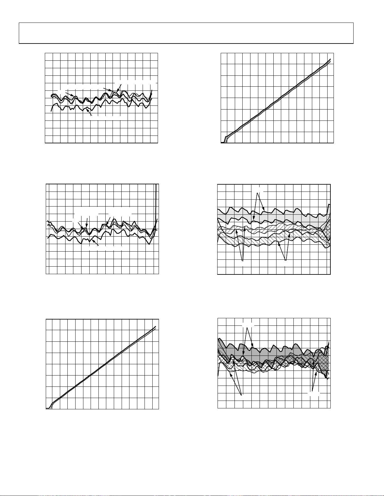
3.8
3.5
3.2
2.9
2.6
2.3
2.0
1.7
VOUT (V)
1.4
1.1
–40°C
0.8
0.5
0.2
–60 –55 –50 –45 –40 –35 –30 –25 –20 –15 –5 0 5 10 15–10
Figure 45. Output Voltage and Law Conformance Error
+25°C
–40°C
+85°C
+25°C
+85°C
INPUT AMPLI TUDE (dBm)
= −40°C, +25°C, and +85°C
@ T
A
3.0
2.5
2.0
1.5
1.0
0.5
0
–0.5
–1.0
–1.5
–2.0
–2.5
–3.0
ERROR IN VOUT ( dB)
Figure 45 shows the output of the circuit of Figure 47 over the
full input range. The agreement with the ideal function (law
conformance) is also shown. This was determined by linear
regression on the data points over the central portion of the
transfer function for the +25°C data.
The error at −40°C, +25°C, and +85°C was then calculated by
subtracting the ideal output voltage at each input signal level
from the actual output and dividing this quantity by the mean
slope of the regression equation to provide a measurement of
the error in decibels (scaled on the right-hand axis of
Figure 45).
The error curves generated in this way reveal not only the deviations from the ideal transfer function at a nominal temperature,
but also the additional errors caused by temperature changes.
Notice that there is a small temperature dependence in the
intercept (the vertical position of the error plots).
Figure 45 further reveals a periodic ripple in the conformance
curves. This is due to the interpolation technique used to select
the signals from the attenuator, not only at discrete tap points,
but anywhere in between, thus providing continuous attenuation values. The selected signal is then applied to the 3.5 GHz,
40 dB fixed gain amplifier in the remaining stages of the VGA
of the AD8362.
02923-045
Rev. D | Page 17 of 32

AD8362
An approximate schematic of the signal input section of the
AD8362 is shown in
Figure 46. The ladder attenuator is composed of 11 sections (12 taps), each of which progressively
attenuates the input signal by 6.33 dB. Each tap is connected to
a variable transconductance cell whose bias current determines
the signal weighting given to that tap. The interpolator determines
which stages are active by generating a discrete set of bias currents,
each having a Gaussian profile. These are arranged to move
from left to right, thereby determining the attenuation applied
to the input signal as the gain is progressively lowered over the
69.3 dB range under control of the VSET input. The detailed
manner in which the transconductance of adjacent stages varies
as the virtual tap point slides along the attenuator accounts for
the ripple observed in the conformance curves. Its magnitude is
slightly temperature dependent and also varies with frequency
(see
Figure 10, Figure 11, and Figure 12). Notice that the system’s
responses to signal inputs at INHI and INLO are not completely
independent; these pins do not constitute a fully floating
differential input.
ATTENUAT ION
CONTROL
TO FIXED
GAIN STAGE
INHI
DECL
INLO
GAUSSIAN INTERPO LATO R
gm gm gm gm
STAGE 1
6.33dB
Figure 46. Simplified Input Circuit
STAGE 2
6.33dB
STAGE 11
6.33dB
OFFSET ELIMINATION
To address the small dc offsets that arise in the VGA, an offsetnulling loop is used. The high-pass corner frequency of this
loop is internally preset to 1 MHz, which is sufficiently low for
02923-046
most high frequency applications. When using the AD8362
in low frequency applications, the corner frequency can be
reduced as needed by the addition of a capacitor from the
CHPF pin to ground having a nominal value of 200 µF/Hz.
For example, to lower the high-pass corner frequency to
150 Hz, a capacitance of 1.33 µF is required. The offset
voltage varies depending on the actual gain at which the
VGA is operating, and thus on the input signal amplitude.
Baseline variations of this sort are a common aspect of all
VGAs, but they are more evident in the AD8362 because of the
method of its implementation, which causes the offsets to ripple
along the gain axis with a period of 6.33 dB. When an excessively large value of CHPF is used, the offset correction process
can lag the more rapid changes in the VGA’s gain, which in turn
can increase the time required for the loop to fully settle for a
given steady input amplitude.
TIME-DOMAIN RESPONSE OF THE CLOSED LOOP
The external low-pass averaging capacitance (CLPF) added at
the output of the squaring cell is chosen to provide adequate
filtering of the fluctuating detected signal. The optimum value
depends on the application; as a guideline, a value of roughly
900 µF/Hz should be used. For example, a capacitance of 5 µF
provides adequate filtering down to 180 Hz. Note that the
fluctuation in the quasi-dc output of a squaring cell operating
on a sine wave input is a raised cosine at twice the signal
frequency, easing this filtering function.
In the standard connections for the measurement mode, the
VSET pin is tied to VOUT. For small changes in input amplitude (a few decibels), the time-domain response of this loop
is essentially linear, with a 3 dB low-pass corner frequency of
nominally f
this local loop set the minimum recommended value of this
capacitor to about 300 pF, resulting in f
When large and abrupt changes of input amplitude occur,
the loop response becomes nonlinear and exhibits slew rate
limitations.
= 1/(CLPF × 1.1 kΩ). Internal time delays around
LP
= 3 MHz.
LP
Rev. D | Page 18 of 32

AD8362
V
OPERATION IN RF MEASUREMENT MODE
BASIC CONNECTIONS
Basic connections for operating the AD8362 in measurement
mode are shown in
Figure 47. While the AD8362 requires a
single supply of nominally 5 V, its performance is essentially
unaffected by variations of up to ±10%.
The supply is connected to the VPOS pin using the decoupling
network also displayed in
Figure 47. The capacitors used in this
network must provide a low impedance over the full frequency
range of the input and should be placed as close as possible to
the VPOS pin. Two different capacitors are used in parallel to
reduce the overall impedance because these have different resonant frequencies. The measurement accuracy is not critically
dependent on supply decoupling because the high frequency
signal path is confined to the relevant input pins. Lead lengths
from both DECL pins to ground and from INHI/INLO to the
input coupling capacitors should be as short as possible. All
COMM pins should also connect directly to the ground plane.
To place the device in measurement mode, connect VOUT to
VSET and connect VTGT directly to VREF.
DEVICE DISABLE
The AD8362 is disabled by a logic high on the PWDN pin,
which can be directly grounded for continuous operation.
When enabled, the supply current is nominally 20 mA and
essentially independent of supply voltage and input signal
strength. When powered down by a logic low on PWDN,
the supply current is reduced to 230 µA.
RECOMMENDED INPUT COUPLING
The full dynamic range of the AD8362, particularly at very
high frequencies (above 500 MHz), is realized only when the
input is presented to it in differential (balanced) form. In
a transmission line balun is used at the input. Having a 1:4
impedance ratio (1:2 turns ratio), the 200 Ω differential input
resistance of the AD8362 becomes 50 Ω at the input to the balun.
AD8362
SIGNAL
INPUT
Z = 50Ω
1:4 Z-RATIO
C10
1000pF
T1
ETC1.6-4-2-3
C6
100pF
C5
100pF
1000pF
Figure 47. Basic Connections for RF Power Measurement
1nF
C8
C4
C7
1nF
1 16
COMM
ACOM
2 15
CHPF
VREF
3 14
DECL
VTGT
4 13
INHI
VPOS
5 12
INLO
VOUT
6 11
DECL
VSET
7 10
PWDN
ACOM
8 9
COMM
CLPF
5V @ 24mA
C3
0.1µF
Figure 47,
S
C1
0.1µF
C2
1nF
V
OUT
02923-047
The balun outputs must be ac-coupled to the input of the
AD8362. The balun used in this example (M/A-COM ETC
1.6-4-2-3) is specified for operation from 0.5 GHz to 2.5 GHz.
If a center-tapped, flux-coupled transformer is used, connect
the center tap to the DECL pins, which are biased to the same
potential as the inputs (~3.6 V).
At lower frequencies where impedance matching is not necessary, the AD8362 can be driven from a low impedance differential
source, remembering the inputs must be ac-coupled.
Choosing Input Coupling Capacitors
As noted, the inputs must be ac-coupled. The input coupling
capacitors combine with the 200 input impedance to create
an input high pass corner frequency equal to
= 1/(200 × π × CC) (12)
f
HP
Typical l y, f
should be set to at least one tenth the lowest input
HP
frequency of interest.
Single-Ended Input Drive
As previously noted, the input stages of the AD8362 are optimally
driven from a fully balanced source, which should be provided
wherever possible. In many cases, unbalanced sources can be
applied directly to one or the other of the two input pins. The
chief disadvantage of this driving method is a 10 dB to 15 dB
reduction in dynamic range at frequencies above 500 MHz.
Figure 48 illustrates one of many ways of coupling the signal
source to the AD8362. Because the input pins are biased to
about 3.6 V (for V
= 5 V), dc-blocking capacitors are required
S
when driving from a grounded source. For signal frequencies
>5 MHz, a value of 1 nF is adequate. While either INHI or
INLO can be used, INHI is chosen here.
AD8362
1 16
COMM
0.01µF
RF INPUT
100Ω
2 15
1nF
3 14
1nF
4 13
1nF
5 12
6 11
1nF
7 10
8 9
Figure 48. Input Coupling from a Single-Ended 50 Ω Source
CHPF
DECL
INHI
INLO
DECL
PWDN
COMM
ACOM
VREF
VTGT
VPOS
VOUT
VSET
ACOM
CLPF
02923-048
Rev. D | Page 19 of 32

AD8362
An external 100 shunt resistor combines with the internal
100 single-ended input impedance to provide a broadband
50 match. The unused input (in this case, INLO) is ac-coupled
to ground.
Figure 49 shows the transfer function of the AD8362
at various frequencies when the RF input is driven singleended. The results show that transfer function linearity at the
top end of the range is degraded by the single-ended drive.
4.0 2.0
3.5 1.5
3.0 1.0
2.5 0.5
2.0 0
VOUT (V)
1.5 –0.5
1.0 –1.0
0.5 –1.5
450MHz
1900MHz
2500MHz
900MHz
2140MHz
0 –2.0
–55 10
–50 –45 –40 –35 –30 –25 –20 –15 –10 –5 0 5
PIN (dBm)
Figure 49. Transfer Function at Various Frequencies when the
RF Input is Driven Single-Ended
AD8362
RF INPUT
2.7nH
4.7nH
1nF
0.01µF
1nF
1nF
1nF
1
2
3
4
5
6
7
8
COMM
CHPF
DECL
INHI
INLO
DECL
PWDN
COMM
ACOM
VREF
VTGT
VPOS
VOUT
VSET
ACOM
CLPF
16
15
14
13
12
11
10
9
Figure 50. Input Matching for Operation at Frequencies ≥2.7 GHz
ERROR (dB)
02923-050
For operation at frequencies ≥2.7 GHz, some additional
components are required to match the AD8362 input to
50 Ω (see
Figure 50). As the operating frequency increases,
there is also corresponding shifting in the operating power
range (see
Figure 51).
3.00
2.75
2.50
2.25
2.00
1.75
1.50
VOUT (V)
1.25
1.00
0.75
0.50
0.25
0
–60 –55 –45 –35 –25 –15 –5 5 15
–50 –40 –30 –20 –10 0 10
INPUT AMPLITUDE (dBm)
2.8GHz
3.45GHz
3.65GHz
3.0
2.5
2.0
1.5
1.0
0.5
0
–0.5
–1.0
–1.5
–2.0
–2.5
–3.0
ERROR (dB)
02923-051
Figure 51. Transfer Function at Various Frequencies ≥2.7 GHz when
the RF Input is Driven Single-Ended
OPERATION AT LOW FREQUENCIES
In conventional rms-to-dc converters based on junction techniques, the effective signal bandwidth is proportional to the
signal amplitude. In contrast, the 3.5 GHz VGA bandwidth in
02923-049
the AD8362 is independent of its gain. Because this amplifier is
internally dc-coupled, the system is also used as a high accuracy
rms voltmeter at low frequencies, retaining its temperaturestable, decibel-scaled output (for example, in seismic, audio,
and sonar instrumentation).
While the AD8362 can be operated at arbitrarily low frequencies,
an ac-coupled input interface must be maintained. In such cases,
the input coupling capacitors should be large enough so that the
lowest frequency components of the signal to be included in the
measurement are minimally attenuated. For example, for a 3 dB
reduction at 1.5 kHz, capacitances of 1 µF are needed because the
input resistance is 100 Ω at each input pin (200 Ω differentially),
and the calculation is 1/(2π × 1.5 kΩ × 100) = 1 F. In addition, to
lower the high-pass corner frequency of the VGA, a large capacitor must be connected between the CHPF pin and ground (see
the
Choosing a Value for CHPF section).
More information on the operation of the AD8362 and other RF
power detectors at low frequency is available in Application Note
AN-691: Operation of RF Detector Products at Low Frequency.
Rev. D | Page 20 of 32

AD8362
CHOOSING A VALUE FOR CHPF
The 3.5 GHz VGA of the AD8362 includes an offset cancellation loop, which introduces a high-pass filter effect in its
transfer function. To properly measure the amplitude of the
input signal, the corner frequency (f
) of this filter must be
HP
well below that of the lowest input signal in the desired
measurement bandwidth frequency. The required value
of the external capacitor is given by
CHPF = 200 F/2(π)f
For operation at frequencies as low as 100 kHz, set f
(fHP in Hz) (13)
HP
to
HP
approximately 25 kHz (CHPF = 8 nF). For frequencies above
approximately 2 MHz, no external capacitance is required
because there is adequate internal capacitance on this node.
CHOOSING A VALUE FOR CLPF
In the standard connections for the measurement mode, the
VSET pin is tied to VOUT. For small changes in input amplitude such as a few decibels, the time-domain response of this
loop is essentially linear with a 3 dB low-pass corner frequency
of nominally f
around this local loop set the minimum recommended value
of this capacitor to about 300 pF, making f
For operation at lower signal frequencies, or whenever the
averaging time needs to be longer, use
CLPF = 900 F/2(π)f
When the input signal exhibits large crest factors, such as a
CDMA or W-CDMA signal, CLPF must be much larger than
might seem necessary. This is due to the presence of significant
low frequency components in the complex, pseudorandom
= 1/(CLPF × 1.1 kΩ). Internal time delays
LP
= 3 MHz.
LP
(fLP in Hz) (14)
LP
modulation, which generates fluctuations in the output of the
AD8362. Increasing CLPF also increases the step response of
the AD8362 to a change at its input.
Tabl e 4 shows recommended values of CLPF for popular
modulation schemes. In each case, CLPF is increased until
residual output noise falls below 50 mV. A 10% to 90% step
response to an input step is also listed. Where the increased
response time is unacceptably high, CLPF must be reduced.
If the output of the AD8362 is sampled by an ADC, averaging
in the digital domain can further reduce the residual noise.
Figure 52 shows how residual ripple and rise/fall time vary with
filter capacitance when the AD8362 is driven by a single carrier
W-CDMA signal (Test Model 1-64) at 2140 MHz.
180 18
170 17
160 16
150 15
RESIDUAL RIPPLE (mV p-p)
140 14
130 13
120 12
110 11
100 10
90 9
80 8
70 7
60 6
50 5
RESIDUAL RIPPLE (mV p-p)
40 4
30 3
20 2
10 1
00
0.10 0.2 0.3 0. 4 0.5 0.6 0.7 0.8 0.9 1.0
Figure 52. Residual Ripple, Rise and Fall Time vs. Filter Capacitance,
Single Carrier W-CDMA Input Signal, Test Model 1-64
FILTER CAPACITANCE (µF )
FALL TIME (ms)
RISE/FALL TIME (ms)
RISE TIME (ms)
02923-052
Table 4. Recommended CLPF Values for Various Modulation Schemes
Response Time (Rise/Fall)
Modulation Scheme/Standard Crest Factor CLPF Residual Ripple
10% to 90%
W-CDMA , Single-Carrier, Test Model 1-64 12.0 dB 0.1 μF 28 mV p-p 171 μs/1.57 ms
W-CDMA 4-Carrier, Test Model 1-64 11.0 dB 0.1 μF 20 mV p-p 162 μs/1.55 ms
CDMA2000, Single-Carrier, 9CH Test Model 9.1 dB 0.1 μF 38 mV p-p 179 μs /1.55 ms
CDMA2000, 3-Carrier, 9CH Test Model 11.0 dB 0.1 μF 29 mV p-p 171 μs/1.55 ms
WiMAX 802.16 (64QAM, 256 Subcarriers, 10 MHz Bandwidth) 14.0 dB 0.1 μF 30 mV p-p 157 μs/1.47 ms
Rev. D | Page 21 of 32

AD8362
ADJUSTING VTGT TO ACCOMMODATE SIGNALS WITH VERY HIGH CREST FACTORS
An external direct connection between VREF (1.25 V) and VTGT
sets up the internal target voltage, which is the rms voltage that
must be provided by the VGA to balance the AGC feedback loop.
In the default scheme, the VREF of 1.25 V positions this target
to 0.06 × 1.25 V = 75 mV. In principle, however, VTGT can be
driven by voltages that are larger or smaller than 75 mV. This
technique can be used to move the intercept, which increases
or decreases the input sensitivity of the device, or to improve
the accuracy when measuring signals with large crest factors.
For example, if this pin is supplied from VREF via a simple
resistive attenuator of 1 kΩ:1 kΩ, the output required from the
VGA is halved to 37.5 mV rms. Under these conditions, the
effective headroom in the signal path that drives the squaring
cell is doubled. In principle, this doubles the peak crest factor
that can be handled by the system.
Figure 53 and Figure 54 show the effect of varying VTGT on
measurement accuracy when the AD8362 is swept with a series
of signals with different crest factors, varying from CW with a
crest factor of 3 dB, to a W-CDMA carrier (Test Model 1-64)
with a crest factor of 10.6 dB. The crest factors of each signal
are listed in the plots. In
value of 1.25 V, while in
4.0
VOUT CW
VOUT 64QAM
3.5
VOUT WCDMA T M1-64
VOUT QPSK
VOUT 256QAM
3.0
2.5
2.0
VOUT (V)
1.5
1.0
0.5 –1.5
0
–65 10
–60 –5 5 –50 –45 –40 –35 –30 –25 –20 –15 –10 –5 0 5
Figure 53. Transfer Function and Law Conformance for Signals with
Figure 53, VTGT is set to its nominal
Figure 54, it is reduced to 0.625 V.
ERROR QPSK 4dB CF
ERROR 256QAM 8.2d B CF
ERROR CW
ERROR 64QAM 7.7d B CF
ERROR WCDMA TM1- 64 10.6dB CF
PIN (dBm)
Varying Crest Factors, VTGT = 1.25 V
2.0
1.5
1.0
0.5
0
–0.5
–1.0
–2.0
ERROR (dB)
4.0
VOUT CW
VOUT 64QAM
3.5
VOUT WCDMA T M1-64
VOUT QPSK
VOUT 256QAM
3.0
2.5
2.0
VOUT (V)
1.5
1.0
0.5 –1.5
0
–65 10
–60 –5 5 –50 –45 –40 –35 –30 –25 –20 –15 –10 –5 0 5
ERROR QPSK 4dB CF
ERROR 256QAM 8.2d B CF
ERROR CW
ERROR 64QAM 7.7d B CF
ERROR WCDMA TM1- 64 10.6dB CF
PIN (dBm)
2.0
1.5
1.0
0.5
0
–0.5
–1.0
–2.0
ERROR (dB)
02923-054
Figure 54. Transfer Function and Law Conformance for Signals with
Varying Crest Factors, VTGT = 0.625 V, CLPF = 0.1 F
Reducing VTGT also reduces the intercept. More significant in
this case, however, is the behavior of the error curves. Note that
in
Figure 54 all of the error curves sit on one another, while in
Figure 53, there is some vertical spreading. This suggests that
VTGT should be reduced in those applications where a wide
range of input crest factors are expected. As noted, VTGT can
also be increased above its nominal level of 1.25 V. While this
can be used to increase the intercept, it would have the undesirable effect of degrading measurement accuracy in situations
where the crest factor of the signal being measured varies
significantly.
ALTERING THE SLOPE
None of the changes in operating conditions discussed so far
affects the logarithmic slope (V
readily be altered by controlling the fraction of VOUT that is
fed back to the setpoint interface at the VSET pin. When the
full signal from VOUT is applied to VSET, the slope assumes
its nominal value of 50 mV/dB. It can be increased by including
a voltage divider between these pins, as shown in
AD8362
1
2
02923-053
3
4
5
6
7
8
Figure 55. External Network to Raise Slope
COMM
CHPF
DECL
INHI
INLO
DECL
PWDN
COMM
ACOM
VREF
VTGT
VPOS
VOUT
VSET
ACOM
CLPF
) in Equation 10. This can
SLP
Figure 55.
16
15
14
13
12
11
10
9
V
R1
R2
OUT
02923-055
Rev. D | Page 22 of 32

AD8362
V
Moderately low resistance values should be used to minimize
scaling errors due to the 70 kΩ input resistance at the VSET
pin. This resistor string also loads the output, and it eventually
reduces the load-driving capabilities if very low values are used.
To calculate the resistor values, use
R1 = R2' (S
/50 − 1) (15)
D
where:
S
is the desired slope, expressed in mV/dB.
D
R2' is the value of R2 in parallel with 70 kΩ.
For example, using R1 = 1.65 kΩ and R2 = 1.69 kΩ (R2' =
1.649 kΩ), the nominal slope is increased to 100 mV/dB.
Note, however, that doubling the slope in this manner reduces
the maximum input signal to approximately −10 dBm because
of the limited swing of VOUT (4.9 V with a 5 V power supply).
TEMPERATURE COMPENSATION AND REDUCTION OF TRANSFER FUNCTION RIPPLE
The transfer function ripple and intercept drift of the AD8362
can be reduced using two techniques detailed in
CLPF is reduced from its nominal value. For broadbandmodulated input signals, this results in increased noise at
the output that is fed back to the VSET pin.
The noise contained in this signal causes the gain of the VGA
to fluctuate around a central point, moving the wiper of the
Gaussian Interpolator back and forth on the R-2R ladder.
Because the gain-control voltage is constantly moving across
at least one of taps of the Gaussian Interpolator, the relationship
between the rms signal strength of the VGA output and the
VGA control voltage becomes independent of the VGA gain
control ripple (see
Figure 56). The signal being applied to the
squaring cell is now lightly AM modulated. However, this does
not change the peak-to-average ratio of the signal.
5
Figure 57.
4.0
3.5
3.0
2.5
2.0
VOUT (V)
1.5
1.0
0.5
0
–60 –40–50 –30 –20 –10 0 10
ERROR (dB –40°C)
V
(+25°C)
OUT
(–40°C)
V
OUT
(+85°C)
V
OUT
PIN (dBm)
ERROR (dB +25° C)
ERROR (dB +85° C)
Figure 56. Transfer Function and Linearity with Combined Ripple Reduction
and Temperature Compensation Circuits, Frequency = 2.14 GHz,
Single-Carrier W-CDMA, Test Model 1-64
Because of the reduced filter capacitor, the rms voltage appearing
at the output of the error amplifier now contains significant
peak-to-peak noise. While it is critical to feed this signal back
to the VGA gain control input with the noise intact, the rms
voltage going to the external measurement node can be filtered
using a simple filter to yield a largely noise-free rms voltage.
The circuit shown in
Figure 57 also incorporates a temperature
sensor that compensates temperature drift of the intercept.
Because the temperature drift varies with frequency, the amount
of compensation required must also be varied using R1 and R2.
These compensation techniques are discussed in more detail in
Application Note
AN-653: Improving Temperature, Stability, and
Linearity of High Dynamic Range RMS RF Power Detectors.
5V
2
1
0
ERROR (dB)
–1
–2
2923-056
0.1µF1nF
VPOS
1
AD8362
COMM
ACOM
1
ADDITIONAL PINS
OMITT ED FOR CLARIT Y.
VOUT
VSET
VREF
VTGT
CLPF
440pF
1kΩ
1µF
3
AD8031
2
1
4
0.1µF
7
6
5
V
R1
R2
TEMP
1
5V
0.1µF
2
TMP36F
5
V
OUT_COMP
FREQUENCY (MHz) R1 (kΩ)R2 (kΩ)
900 1.02 25.5
1900 1 82.5
2200 1 19.1
02923-057
Figure 57. Temperature Compensation and Reduction of Transfer Function Ripple
Rev. D | Page 23 of 32

AD8362
TEMPERATURE COMPENSATION AT VARIOUS WiMAX FREQUENCIES UP TO 3.8 GHz
The AD8362 is ideally suited for measuring WiMAX type
signals because crest factor changes in the modulation scheme
have very little affect on the accuracy of the measurement.
However, at higher frequencies, the AD8362 drifts more over
temperature often making temperature compensation necessary.
Temperature compensation is possible because the part-to-part
variation over temperature is small, and temperature change
only causes a shift in the AD8362’s intercept. Typically, users
choose to compensate for temperature changes digitally. However, temperature compensation is possible using an analog
temperature sensor. Because the drift of the output voltage is
due mainly to intercept shift, the whole transfer function tends
to drop with increasing temperature, while the slope remains
quite stable. This makes the temperature drift independent of
input level. Compensating the drift based on a particular
input level (for example, −15 dBm), holds up well over the
dynamic range.
Figure 59 through Figure 63 show these results. The compensation is simple and relies on the TMP36 precision temperature
sensor driving one side of the resistor divider as the AD8362
drives the other side. The output is at the junction of the two
resistors (see Figure 58). At 25°C, TMP36 has an output voltage
of 750 mV and a temperature coefficient of 10 mV/°C. As the
temperature increases, the voltage from the AD8362 drops and
the voltage from the TMP36 rises. R1 and R2 are chosen so the
voltage at the center of the resistor divider remains steady over
temperature. In practice, R2 is much larger than R1 so that the
output voltage from the circuit is close to the voltage of the V
OUT
pin. The resistor ratio R2/R1 is determined by the temperature
drift of the AD8362 at the frequency of interest. To calculate the
values of R1 and R2, first calculate the drift at a particular input
level, −15 dBm in this case. To do this, calculate the average
drift over the temperature range from 25°C to 85°C. Using the
following equation, the average drift in dB/°C is obtained.
Error
dB
CdB/ =° (16)
Δ
eTemperatur
Table 5 shows the resultant values for R2 and R1 for frequen
cies ranging from 2350 MHz to 3650 MHz. Figure 59 through
Figure 63 show the performance over temperature for the
AD8362 with temperature compensation at frequencies across
the WiMAX band. The compensation factor chosen optimizes
temperature drift in the 25°C to 85°C range. This can be altered
depending on the temperature requirements for the application.
Table 5. Recommended Resistor Values for Temperature
Compensation at Various Frequencies
Freq.
(MHz)
Average
Drift @
−15 dBm
(dB/°C)
Slope
(mV/dB)
Average
Drift @
−15 dBm
(mV/°C)
R1
(kΩ)
2350 −0.0345 51 −1.7600 4.99 28
2600 −0.0440 51.45 −2.2639 4.99 22.1
2800 −0.0486 51.68 −2.5102 4.99 20
3450 −0.0531 51.61 −2.7402 4.99 18.2
3650 −0.0571 51.73 −2.9544 4.99 16.9
1nF
AD8362
INHI
VOUT
VSET
INLO
CLPF
VTGT VREF
R1 R2
0.1µF
V
OUT
V
TEMP
1
TMP36F
2.7nH
1nF
4.7nH
Figure 58. AD8362 with Temperature Compensation Circuit
-
R2
(kΩ)
5V
0.1µF
2
5
02923-058
In this example, the drift of the AD8362 from 25°C to 85°C is
−2.07 dB and the temperature delta is 60°C, which results in
−0.0345 dB/°C drift. This temperature drift in dB/°C is converted to mV/°C through multiplication by the logarithmic slope
(51 mV/dB at 2350 MHz). The result is −1.76 mV/°C. The
following equation calculates the values of R1 and R2:
R2
=
CmV/10°°
DriftAD8362R1
(17)
C)(mV/
Rev. D | Page 24 of 32

AD8362
4.0
3.5
3.0
2.5
2.0
VOUT (V)
1.5
1.0
0.5
0
–60 20
–50 –40 –30 –20 –10 0 10
INPUT AMPLITUDE (dBm)
Figure 59. AD8362 VOUT and Error with Linear Temperature
Compensation at 2350 MHz
4.0
3.5
3.0
2.5
2.0
VOUT (V)
1.5
1.0
0.5
0
–60 20
–50 –40 –30 –20 –10 0 10
INPUT AMPLITUDE (dBm)
+85°C
+25°C
–40°C
+85°C
+25°C
–40°C
8
6
4
2
0
ERROR (dB)
–2
–4
–6
–8
02923-059
4.0
3.5
3.0
2.5
2.0
VOUT (V)
1.5
1.0
0.5
0
–60 20
–50 –40 –30 –20 –10 0 10
INPUT AMPLITUDE (dBm)
+85°C
+25°C
–40°C
8
6
4
2
0
ERROR (dB)
–2
–4
–6
–8
02923-062
Figure 62. AD8362 VOUT and Error with Linear Temperature
Compensation at 3450 MHz
8
6
4
2
0
ERROR (dB)
–2
–4
–6
–8
02923-060
4.0
3.5
3.0
2.5
2.0
VOUT (V)
1.5
1.0
0.5
0
–60 20
–50 –40 –30 –20 –10 0 10
INPUT AMPLITUDE (dBm)
+125°C
+105°C
+85°C
+25°C
–40°C
8
6
4
2
0
ERROR (dB)
–2
–4
–6
–8
02923-063
Figure 60. AD8362 VOUT and Error with Linear Temperature
Compensation at 2600 MHz
4.0
3.5
3.0
2.5
2.0
VOUT (V)
1.5
1.0
0.5
0
–60 20
–50 –40 –30 –20 –10 0 10
INPUT AMPLITUDE (dBm)
Figure 61. AD8362 VOUT and Error with Linear Temperature
Compensation at 2800 MHz
+85°C
+25°C
–40°C
8
6
4
2
0
ERROR (dB)
–2
–4
–6
–8
02923-061
Rev. D | Page 25 of 32
Figure 63. AD8362 VOUT and Error with Linear Temperature Compensation
at 3650 MHz, Temperature Compensation is Optimized for 85°C

AD8362
OPERATION IN CONTROLLER MODE
The AD8362 provides a controller mode feature at the VOUT
pin. Using VSET for the setpoint voltage, it is possible for the
AD8362 to control subsystems such as power amplifiers (PAs),
VGAs, or variable voltage attenuators (VVAs), which have
output power that decreases monotonically with respect to
their (increasing) gain control signal.
CONTROLLED SYST EM
(OUTPUT POWER
DECREASES AS
P
OUT
OUTPUT CONTROL VOLTAGE
ATTN
C10
1000pF
1:4 Z-RATIO
T1
ETC1.6-4-2-3
C6
100pF
C5
100pF
1000pF
C4
1nF
C8
C7
1nF
Figure 64. Basic Connections for Controller Mode Operation
VAPC INCREASES)
VAPC
0.1V TO 4.9V
AD8362
1 16
COMM
ACOM
2 15
CHPF
VREF
3 14
DECL
VTGT
4 13
INHI
VPOS
5 12
INLO
VOUT
6 11
DECL
VSET
7 10
PWDN
ACOM
8 9
COMM
CLPF
(SEE TEXT)
C3
INPUTOUTPUT
V
S
0.1µF
SETPOINT
VOLTAGE
INPUT
0V TO 3. 5V
C1
C2
1nF
P
IN
02923-064
To operate in controller mode, the link between VSET and
VOUT is broken. A setpoint voltage is applied to the VSET
input, while VOUT is connected to the gain control terminal
of the VGA, and the AD8362 RF input is connected to the output of the VGA (generally using a directional coupler or power
splitter and some additional attenuation). Based on the defined
relationship between VOUT and the RF input signal when the
device is in measurement mode, the AD8362 adjusts the voltage
on VOUT (VOUT is now an error amplifier output) until the
level at the RF input corresponds to the applied VSET. For
example, in a closed loop system, if VSET is set to 3 V, VOUT
increases or decreases until the input signal is equal to 0 dBm.
This relationship follows directly from the measurement mode
transfer function (see
Figure 10, Figure 11, and Figure 12).
Therefore, when the AD8362 operates in controller mode, there
is no defined relationship between VSET and VOUT. VOUT
settles to a value that results in balance between the input signal
levels appearing at INHI/INLO and VSET.
For this output power control loop to be stable, a groundreferenced capacitor must be connected to the CLPF pin.
This capacitor integrates the internal error current that is
present when the loop is not balanced.
Increasing VSET, which corresponds to demanding a higher
signal from the VGA, tends to decrease VOUT. The VGA or VVA
therefore must have a negative sense. In other words, increasing
the gain control voltage decreases gain. If this is not the case, an
op amp, configured as an inverter with suitable level shifting, can
be used to correct the sense of the VOUT signal.
Rev. D | Page 26 of 32

AD8362
V
RMS VOLTMETER WITH 90 dB DYNAMIC RANGE
The 65 dB range of the AD8362 can be extended by adding a
standalone VGA as a preamplifier whose gain control input is
derived directly from VOUT. This extends the dynamic range
by the gain control range of this second amplifier. When this
VGA also provides a linear-in-dB (exponential) gain control
function, the overall measurement remains linearly scaled in
decibels. The VGA gain must decrease with an increase in its
gain bias in the same way as the AD8362. Alternatively, an
inverting op amp with suitable level shifting can be used. It is
convenient to select a VGA needing only a single 5 V supply
and capable of generating a fully balanced differential output.
All of these conditions are met by the
the schematic. Also, note that the
single-ended input into the differential-ended input needed by
the
AD8330. The AD8131’s gain of 2 does create a dc offset on
the output of the AD8362, but this is removed by connecting
0.5 V to the VMAG on
AD8330.
Using the inverse gain mode (MODE pin low) of the
its gain decreases on a slope of 30 mV/dB to a minimum value
of 3 dB for a gain voltage (VDBS) of 1.5 V. VDBS is 40% of the
output of the AD8362. Over the 3 V range from 0.5 V to 3.5 V,
the gain of the
AD8330 varies by (0.4 × 3 V)/(30 mV/dB), or
40 dB. Combined with the 65 dB gain span of the AD8362, this
results in a 100 dB variation for a 3 V change in VOUT. Due to
the noise generated from the
AD8330, the dynamic range is
AD8330. Figure 66 shows
AD8131 is used to convert a
AD8330,
limited to approximately 90 dB. This can only be achieved when
a band-pass filter is used at the operating frequency between
the
AD8330 and AD8362.
Figure 65 shows data results of the extended dynamic range at
70 MHz with error in VOUT.
–93
–80
–83
–70
–103
3.0 6
2.5 4
2.0 2
1.5 0
OUTPUT (V)
1.0 –2
0.5 –4
0–
–90
–73
–60
INPUT (dBV)
–63
–53
–50
–40
INPUT (dBm)
–43
–30
–33
–20
–230–1310–3
–10
Figure 65. Output and Conformance for the AD8330/AD8362
Extended Dynamic Range Circuit
7
ERROR IN VOUT (dB)
6
20
+5
02923-065
0.1µF
0.1µF
0.1µF
OFSTENBL CNTRVPOS
VPS1 VPSO
INHI OPHI
AD8330
INLO OPLO
MODE CMOP
VMAGCOMMCMGNVDBS
+0.5V
10µF
BAND-PASS
@ 70MHz
0.1µF
1
2
3
4
5
6
7
8
AD8362
COMM
CHPF
DECL
INHI
INLO
DECL
PWDN
COMM
ACOM
VREF
VTGT
VPOS
VOUT
VSET
ACOM
CLPF
10µF
0.1µF
2kΩ
2kΩ
V
OUT
02923-066
16
15
14
13
12
11
10
9
INPUT
49.9Ω
GAIN OF 2
0.1µF
AD8131
29.9Ω
0.1µF
–5V
0.01µF
0.1µF
3
8
4
2
1
5
6
0.1µF
0.01µF
Figure 66. RMS Voltmeter with 90 dB Dynamic Range
Rev. D | Page 27 of 32

AD8362
AD8362 EVALUATION BOARD
The AD8362 evaluation board provides for a number of different operating modes and configurations, including many
described in this data sheet. The measurement mode is set up
by positioning SW2 as shown in
Figure 67. The AD8362 can be
operated in controller mode by applying the setpoint voltage to
the VSET connector, and flipping SW2 to its alternate position.
The internal voltage reference is used for the target voltage when
SW1 is in the position shown in
Figure 67. This voltage may
optionally be reduced via a voltage divider implemented with
R4 and R5, with LK1 in place, and SW1 switched to its alternate
position. Alternatively, an external target voltage may be used
RFIN
PWDN
C10
1000pF
AGND
R14
OPEN
1000pF
T1
SW3
R13
10kΩ
C8
100pF
100pF
R15
0Ω
1000pF
C6
R16
OPEN
C5
1000pF
VPOS
1
2
C7
3
4
5
C4
6
7
8
Figure 67. Evaluation Board Schematic
0.1µF
COMM
CHPF
DECL
INHI
INLO
DECL
PWDN
COMM
C1
AD8362
with SW1 switched to its alternate position, LK1 removed, and
the external target voltage applied to the VTGT connector.
In measurement mode, the slope of the response at VOUT may
be increased by using a voltage divider implemented with resistors in Position R17 and Position R9, and with SW2 switched to
its alternate position.
The AD8362 is powered up with SW3 in the position shown in
Figure 67 and connector PWDN open. The part can be powered
down by either connecting a logic high voltage to a connector,
PWDN, with SW3 in the position, or by switching SW3 to its
alternate position.
R1
0Ω
C2
100pF
ACOM
VREF
VTGT
VPOS
VOUT
VSET
ACOM
CLPF
16
15
14
13
12
11
10
9
R17
OPEN
R10
0Ω
R6
0Ω
R9
10kΩ
R8
0Ω
C3
0.1µF
C9
OPEN
R4
0Ω
SW1
SW2
R5
10kΩ
VREF
LK1
VTGT
R7
0Ω
VOUT
VSET
2923-067
Rev. D | Page 28 of 32

AD8362
02923-068
Figure 68. Component Side Metal of Evaluation Board
Figure 69. Component Side Silkscreen of Evaluation Board
Rev. D | Page 29 of 32
02923-069

AD8362
Table 6. Bill of Materials
Designator Description Part Number Default Value
T1
C1 Supply filtering/decoupling capacitor 0.1 μF
C2 Supply filtering/decoupling capacitor 100 pF
C3, C9 Output low-pass filter capacitor C3 = 0.1 μF, C9 = open
C4, C7, C10 Input bias-point decoupling capacitors 1000 pF
C5, C6 Input signal coupling capacitors 100 pF
C8 Input high-pass filter capacitor 1000 pF
DUT AD8362 AD8362ARU
LK1 Use to reduce VTGT or to externally apply a voltage to VTGT LK1 = open
R1, R6, R7, R8, R10, R15 Jumpers 0 Ω
R4, R5 Use to reduce VTGT or to externally apply a voltage to VTGT R4 = 0 Ω, R5 = 10 kΩ
R9, R17 Slope adjustment resistors (see the Altering the Slope section) R9 = 10 kΩ, R17 = open
R13 Power-up terminating resistor R13 = 10 kΩ
R16 Not installed Open
SW1 Use to reduce VTGT or to externally apply a voltage to VTGT SW1 connects VREF to VTGT
SW2 Measurement mode/controller mode selector SW2 connects VSET to VOUT
SW3 Power-down/power-up or external power-down selector SW3 connects PWDN to R13
ETC 1.6-4-2-3
(M/A-COM)
Rev. D | Page 30 of 32

AD8362
OUTLINE DIMENSIONS
5.10
5.00
4.90
0.15
0.05
4.50
4.40
4.30
PIN 1
16
0.65
BSC
COPLANARITY
COMPLIANT TO JEDEC STANDARDS MO-153-AB
0.10
0.30
0.19
9
81
1.20
MAX
SEATING
PLANE
6.40
BSC
0.20
0.09
8°
0°
0.75
0.60
0.45
Figure 70. 16-Lead Thin Shrink Small Outline Package [TSSOP]
(RU-16)
Dimensions shown in millimeters
ORDERING GUIDE
Model Temperature Range Package Description Package Option
AD8362ARU −40°C to +85°C 16-Lead TSSOP, Tube RU-16
AD8362ARU-REEL −40°C to +85°C 16-Lead TSSOP, 13" Tape and Reel RU-16
AD8362ARU-REEL7 −40°C to +85°C 16-Lead TSSOP, 7" Tape and Reel RU-16
AD8362ARUZ
AD8362ARUZ-REEL7
AD8362-EVALZ
1
Z = RoHS Compliant Part.
1
1
1
−40°C to +85°C 16-Lead TSSOP, Tube RU-16
−40°C to +85°C 16-Lead TSSOP, 7" Tape and Reel RU-16
Evaluation Board
Rev. D | Page 31 of 32

AD8362
NOTES
©2003–2007 Analog Devices, Inc. All rights reserved. Trademarks and
registered trademarks are the property of their respective owners.
D02923-0-6/07(D)
Rev. D | Page 32 of 32
 Loading...