Analog Devices AD8361 Datasheet

LF to 2.5 GHz
a
FEATURES
Calibrated RMS Response
Excellent Temperature Stability
Up to 30 dB Input Range at 2.5 GHz
700 mV rms, 10 dBm re 50 ⍀ Maximum Input
ⴞ0.25 dB Linear Response Up to 2.5 GHz
Single Supply Operation: 2.7 V to 5.5 V
Low Power: 3.3 mW at 3 V Supply
Rapid Power-Down to Less than 1 A
APPLICATIONS
Measurement of CDMA, W-CDMA, QAM, Other
Complex Modulation Waveforms
RF Transmitter or Receiver Power Measurement
PRODUCT DESCRIPTION
The AD8361 is a mean-responding power detector for use in highfrequency receiver and transmitter signal chains, up to 2.5 GHz.
It is very easy to apply. It requires only a single supply between
2.7 V and 5.5 V, power supply decoupling capacitor and an
input coupling capacitor in most applications. The output is a
linear-responding dc voltage with a conversion gain of 7.5 V/V rms.
An external filter capacitor can be added to increase the averaging time constant.
RFIN
PWDN
RFIN
™
TruPwr
Detector
AD8361
FUNCTIONAL BLOCK DIAGRAMS
micro_SOIC
2
TRANSCONDUCTANCE
CELLS
TRANSCONDUCTANCE
CELLS
2
2
2
i
i
BAND-GAP
REFERENCE
SOT-23-6L
i
i
ERROR
AMP
ERROR
AMP
INTERNAL FILTER
AD8361
IREF
INTERNAL FILTER
AD8361
ⴛ 7.5
BUFFER
OFFSET
ⴛ 7.5
BUFFER
VPOS
FLTR
VRMS
ADD
SREF
COMM
VPOS
FLTR
VRMS
3.0
2.8
2.6
2.4
2.2
2.0
1.8
1.6
1.4
1.2
V rms – Volts
1.0
0.8
0.6
0.4
0.2
0.0
0
SUPPLY
REFERENCE MODE
INTERNAL
REFERENCE MODE
REFERENCE MODE
RFIN – V rms
GROUND
0.50.1 0.2 0.3 0.4
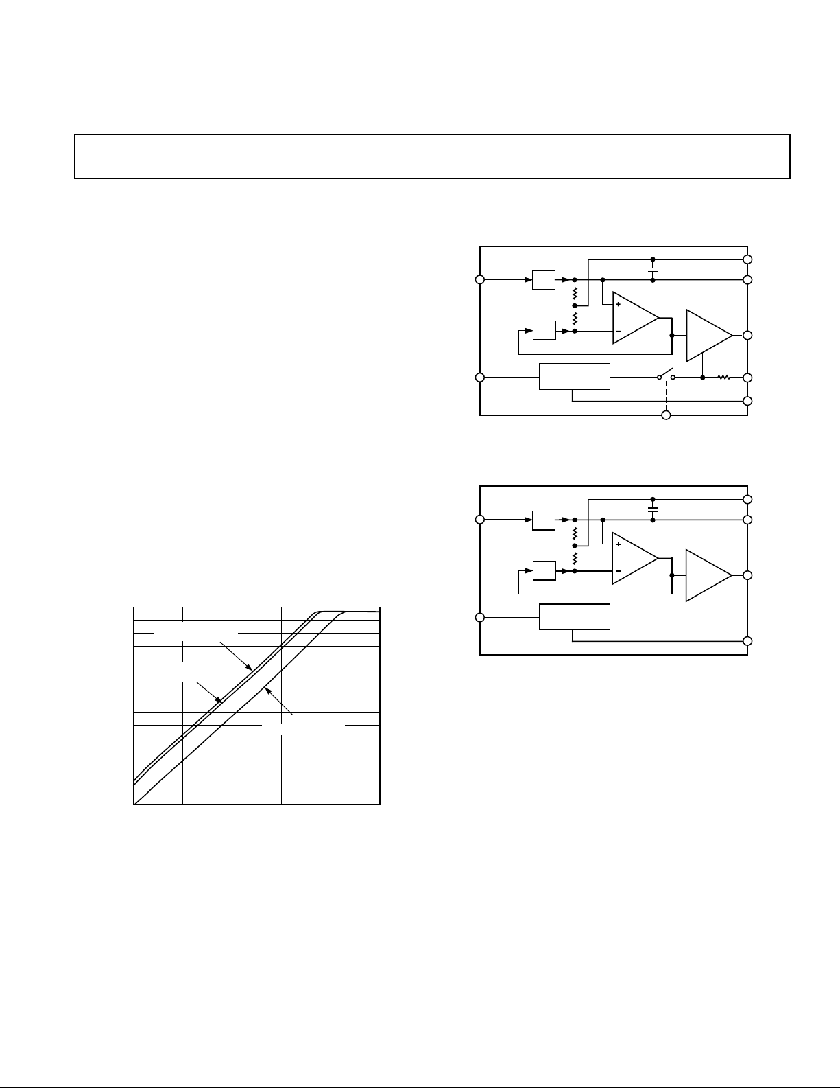
Figure 1. Output in the Three Reference Modes, Supply 3 V,
Frequency 1.9 GHz (SOT-23-6L Package Ground Reference
Mode Only)
TruPwr is a trademark of Analog Devices, Inc.
REV. A
Information furnished by Analog Devices is believed to be accurate and
reliable. However, no responsibility is assumed by Analog Devices for its
use, nor for any infringements of patents or other rights of third parties
which may result from its use. No license is granted by implication or
otherwise under any patent or patent rights of Analog Devices.
PWDN
BAND-GAP
REFERENCE
COMM
The AD8361 is intended for true power measurement of simple
and complex waveforms. The device is particularly useful for
measuring high crest-factor (high peak-to-rms ratio) signals, such
as CDMA and W-CDMA.
The AD8361 has three operating modes to accommodate a
variety of analog-to-digital converter requirements:
1. Ground referenced mode, in which the origin is zero;
2. Internal reference mode, which offsets the output 350 mV
above ground;
3. Supply reference mode, which offsets the output to V
/7.5.
S
The AD8361 is specified for operation from –40°C to +85°C and
is available in 8-lead micro_SOIC and 6-lead SOT packages.
It is fabricated on a proprietary high f
One Technology Way, P.O. Box 9106, Norwood, MA 02062-9106, U.S.A.
Tel: 781/329-4700 World Wide Web Site: http://www.analog.com
Fax: 781/326-8703 © Analog Devices, Inc., 2000
silicon bipolar process.
T

(TA = 25ⴗC, VS = 3 V, fRF = 900 MHz, ground reference output mode, unless otherwise
AD8361–SPECIFICATIONS
Parameter Condition Min Typ Max Unit
SIGNAL INPUT INTERFACE (Input RFIN)
Frequency Range
Linear Response Upper Limit V
Input Impedance
RMS CONVERSION (Input RFIN to Output V rms)
Conversion Gain 7.5 V/V rms
Dynamic Range Error Referred to Best Fit Line
±0.25 dB Error
±1 dB Error CW Input, –40°C < T
±2 dB Error CW Input, –40°C < T
Intercept-Induced Dynamic Internal Reference Mode 1 dB
Range Reduction
Deviation from CW Response 5.5 dB Peak-to-Average Ratio (IS95 Reverse Link) 0.2 dB
OUTPUT INTERCEPT
Ground Reference Mode (GRM) 0 V at SREF, VS at IREF 0 V
Internal Reference Mode (IRM) 0 V at SREF, IREF Open 350 mV
Supply Reference Mode (SRM) 0 V at IREF, 3 V at SREF 400 mV
POWER-DOWN INTERFACE
PWDN HI Threshold 2.7 ≤ VS ≤ 5.5 V, –40°C < TA < +85°CV
PWDN LO Threshold 2.7
Power-Up Response Time 2 pF at FLTR Pin, 224 mV rms at RFIN 5 µs
PWDN Bias Current <1 µA
POWER SUPPLIES
Operating Range –40°C < TA < +85°C2.75.5V
Quiescent Current 0 mV rms at RFIN, PWDN Input LO
Power-Down Current GRM or IRM, 0 mV rms at RFIN, PWDN Input HI <1 µA
NOTES
1
Operation at arbitrarily low frequencies is possible; see Applications section.
2
Figure 13 and Figure 40 show impedance vs. frequency for the micro_SOIC and SOT respectively.
3
Calculated using linear regression.
4
Compensated for output reference temperature drift; see Applications section.
5
SOT-23-6L operates in ground reference mode only.
6
The available output swing, and hence the dynamic range, is altered by both supply voltage and reference mode; see Figures 35 and 36.
7
Supply current is input level dependant; see Figure 12.
Specifications subject to change without notice.
1
= 3 V 390 mV rms
S
Equivalent dBm re 50 Ω 4.9 dBm
= 5 V 660 mV rms
V
S
2
4
Equivalent dBm re 50 Ω 9.4 dBm
f
= 100 MHz, VS = 5 V 6.5 8.5 V/V rms
RF
CW Input, –40°C < TA < +85°C14dB
CW Input, V
5, 6
Supply Reference Mode, VS = 3.0 V 1 dB
Supply Reference Mode, V
12 dB Peak-to-Average Ratio (W-CDMA 4 Channels) 1.0 dB
18 dB Peak-to-Average Ratio (W-CDMA 15 Channels) 1.2 dB
5
Inferred from Best Fit Line
f
= 100 MHz, VS = 5 V –50 +150 mV
RF
= 100 MHz, VS = 5 V 300 500 mV
f
RF
fRF = 100 MHz, VS = 5 V 590 750 mV
0 V at IREF, VS at SREF VS/7.5 V
≤
VS ≤ 5.5 V, –40°C < TA < +85°C0.1V
100 nF at FLTR Pin, 224 mV rms at RFIN 320 µs
SRM, 0 mV rms at RFIN, PWDN Input HI 10 × V
noted.)
2.5 GHz
225储1 Ω储pF
3
< +85°C23dB
A
< +85°C26dB
= 5 V, –40°C < TA < +85°C30dB
S
A
= 5.0 V 1.5 dB
S
3
– 0.5 V
S
7
1.1 mA
S
µA
–2–
REV. A

AD8361
WARNING!
ESD SENSITIVE DEVICE
ABSOLUTE MAXIMUM RATINGS
1
Supply Voltage VS . . . . . . . . . . . . . . . . . . . . . . . . . . . . . 5.5 V
SREF, PWDN . . . . . . . . . . . . . . . . . . . . . . . . . . . . . . . 0 V, V
IREF . . . . . . . . . . . . . . . . . . . . . . . . . . . . . . . . . VS – 0.3 V, V
S
S
RFIN . . . . . . . . . . . . . . . . . . . . . . . . . . . . . . . . . . . . . . 1 V rms
Equivalent Power re 50 Ω . . . . . . . . . . . . . . . . . . . 13 dBm
Internal Power Dissipation
2
. . . . . . . . . . . . . . . . . . . . 200 mW
SOT-23-6L . . . . . . . . . . . . . . . . . . . . . . . . . . . . . . 170 mW
micro_SOIC . . . . . . . . . . . . . . . . . . . . . . . . . . . . . . 200 mW
Maximum Junction Temperature . . . . . . . . . . . . . . . . . 125°C
Operating Temperature Range . . . . . . . . . . . –40°C to +85°C
Storage Temperature Range . . . . . . . . . . . . –65°C to +150°C
Lead Temperature Range (Soldering 60 sec) . . . . . . . . . 300°C
NOTES
1
Stresses above those listed under Absolute Maximum Ratings may cause perma-
nent damage to the device. This is a stress rating only; functional operation of the
device at these or any other conditions above those indicated in the operational
section of this specification is not implied. Exposure to absolute maximum rating
conditions for extended periods may affect device reliability.
2
Specification is for the device in free air.
SOT-23-6L: θJA = 230°C/W; θJC = 92°C/W.
micro_SOIC: θJA = 200°C/W; θJC = 44°C/W.
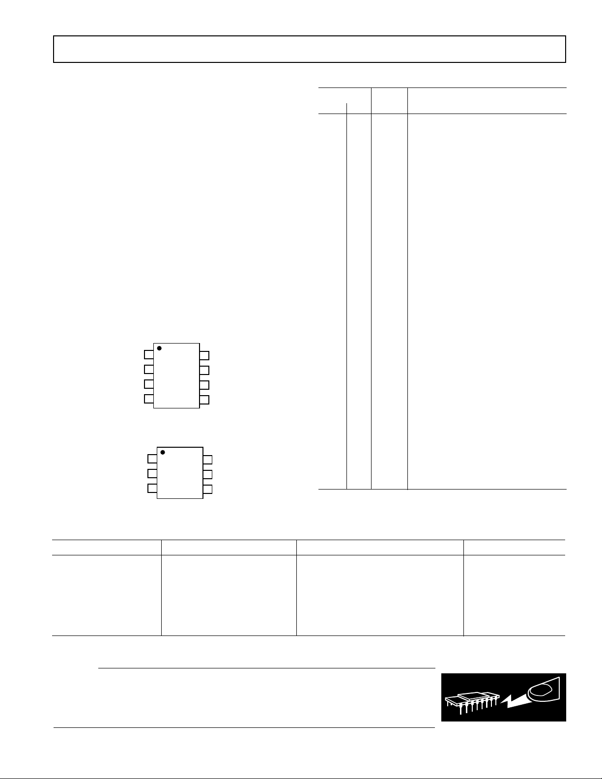
PIN CONFIGURATIONS
micro_SOIC
VPOS
IREF
RFIN
PWDN
1
2
3
4
AD8361
8
7
6
5
SREF
VRMS
FLTR
COMM
SOT-23-6L
VRMS
COMM
FLTR
1
2
3
AD8361
6
5
4
VPOS
RFIN
PWDN
PIN FUNCTION DESCRIPTIONS
Pin
Micro SOT Name Description
1 6 VPOS Supply Voltage Pin. Operational range
2.7 V to 5.5 V.
2 IREF Output Reference Control Pin. Inter-
nal reference mode enabled when pin
is left open. Otherwise, this pin should
be tied to VPOS. DO NOT ground this
pin.
3 5 RFIN Signal Input Pin. Must be driven from
an ac-coupled source. The low frequency
real input impedance is 225 Ω.
4 4 PWDN Power-Down Pin. For the device to
operate as a detector it needs a logical
low input (less than 100 mV). When
a logic high (greater than V
– 0.5 V)
S
is applied, the device is turned off and
the supply current goes to nearly zero
(ground and internal reference mode
less than 1 µA, supply reference mode
divided by 100 kΩ).
V
S
5 2 COMM Device Ground Pin.
6 3 FLTR By placing a capacitor between this pin
and VPOS, the corner frequency of the
modulation filter is lowered. The onchip filter is formed with 27 pF储2 kΩ
for small input signals.
7 1 VRMS Output Pin. Near-rail-to-rail voltage
output with limited current drive capabilities. Expected load >10 kΩ to ground.
8 SREF Supply Reference Control Pin. To en-
able supply reference mode this pin
must be connected to VPOS, otherwise it should be connected to COMM
(ground).
ORDERING GUIDE
Model Temperature Range Package Description Package Option
AD8361ARM* –40°C to +85°C Tube, 8-Lead micro_SOIC RM-8
AD8361ARM-REEL 13" Tape and Reel
AD8361ARM-REEL7 7" Tape and Reel
AD8361ART-REEL 13" Tape and Reel RT-6
AD8361ART-REEL7 7" Tape and Reel
AD8361-EVAL Evaluation Board micro_SOIC
AD8361ART-EVAL Evaluation Board SOT-23-6L
*Device branded as J3A.
CAUTION
ESD (electrostatic discharge) sensitive device. Electrostatic charges as high as 4000 V readily
accumulate on the human body and test equipment and can discharge without detection. Although
the AD8361 features proprietary ESD protection circuitry, permanent damage may occur on
devices subjected to high-energy electrostatic discharges. Therefore, proper ESD precautions are
recommended to avoid performance degradation or loss of functionality.
REV. A
–3–

AD8361
–Typical Performance Characteristics
2.8
2.6
2.4
2.2
2.0
1.8
1.6
1.4
1.2
1.0
OUTPUT – Volts
0.8
0.6
0.4
0.2
0.0
0
900MHz
100MHz
INPUT – V rms
1900MHz
2.5GHz
0.50.1 0.2 0.3 0.4
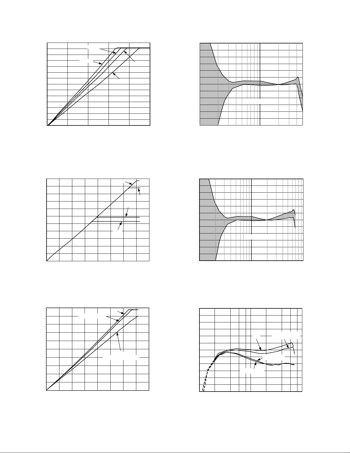
Figure 2. Output vs. Input Level, Frequencies 100 MHz,
900 MHz, 1900 MHz, and 2500 MHz, Supply 2.7 V, Ground
Reference Mode, micro_SOIC
5.5
5.0
4.5
4.0
3.5
3.0
2.5
2.0
OUTPUT – Volts
1.5
1.0
0.5
0.0
0
INPUT – V rms
5.5V
2.7V
0.6 0.7 0.8
0.50.1 0.2 0.3 0.4
5.0V
3.0V
Figure 3. Output vs. Input Level, Supply 2.7 V, 3.0 V, 5.0 V,
and 5.5 V, Frequency 900 MHz
3.0
2.5
2.0
1.5
1.0
0.5
0
–0.5
ERROR – dB
–1.0
–1.5
–2.0
–2.5
–3.0
0.01
0.02
(–21dBm)
MEAN ⴞ3 SIGMA
0.1
(–7dBm)
INPUT – V rms
0.4
(+5dBm)
Figure 5. Error from Linear Reference vs. Input Level,
3 Sigma to Either Side of Mean, Sine Wave, Supply 3.0 V,
Frequency 900 MHz
3.0
2.5
2.0
1.5
1.0
0.5
0
–0.5
ERROR – dB
–1.0
–1.5
–2.0
–2.5
–3.0
0.01
0.02
(–21dBm)
MEAN ⴞ3 SIGMA
0.1
(–7dBm)
INPUT – V rms
0.6
(+8.6dBm)
Figure 6. Error from Linear Reference vs. Input Level,
3 Sigma to Either Side of Mean, Sine-Wave, Supply 5.0 V,
Frequency 900 MHz
5.0
4.5
4.0
3.5
3.0
2.5
2.0
OUTPUT – Volts
1.5
1.0
0.5
0.0
IS95
REVERSE LINK
0
INPUT – V rms
CW
WCDMA
4- AND 15-CHANNEL
0.50.1 0.2 0.3 0.4
0.6 0.7 0.8
Figure 4. Output vs. Input Level with Different Waveforms
Sine Wave (CW), IS95 Reverse Link, W-CDMA 4-Channel
and W-CDMA 15-Channel, Supply 5.0 V
3.0
2.5
2.0
ERROR – dB
1.5
1.0
0.5
0.0
–0.5
–1.0
–1.5
–2.0
–2.5
–3.0
CW
4-CHANNEL
15-CHANNEL
0.02 0.6
INPUT – V rms
0.2
IS95
REVERSE LINK
Figure 7. Error from CW Linear Reference vs. Input with
Different Waveforms Sine Wave (CW), IS95 Reverse Link,
W-CDMA 4-Channel and W-CDMA 15-Channel, Supply
3.0 V, Frequency 900 MHz
–4–
1.00.01 0.1
REV. A

AD8361
3.0
2.5
2.0
1.5
1.0
0.5
0
–0.5
ERROR – dB
–1.0
–1.5
–2.0
–2.5
–3.0
0.01
0.02
(–21dBm)
MEAN ⴞ3 SIGMA
0.1
(–7dBm)
INPUT – V rms
0.4
(+5dBm)
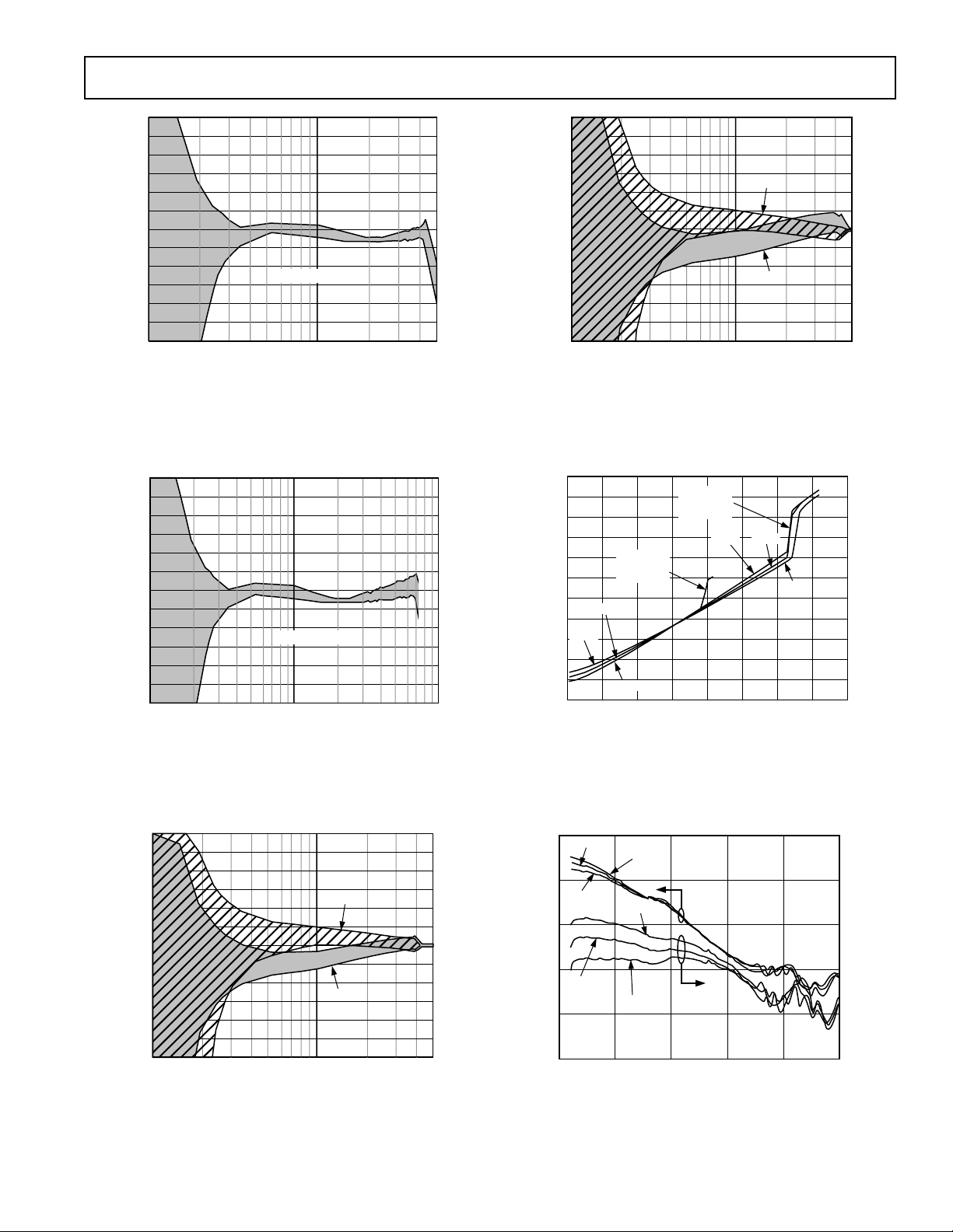
Figure 8. Error from CW Linear Reference vs. Input,
3 Sigma to Either Side of Mean, IS95 Reverse Link Signal,
Supply 3.0 V, Frequency 900 MHz
3.0
2.5
2.0
1.5
1.0
0.5
0
–0.5
ERROR – dB
–1.0
–1.5
–2.0
–2.5
–3.0
0.01
0.02
(–21dBm)
MEAN ⴞ3 SIGMA
0.1
(–7dBm)
INPUT – V rms
0.6
(+8.6dBm)
Figure 9. Error from CW Linear Reference vs. Input Level,
3 Sigma to Either Side of Mean, IS95 Reverse Link Signal,
Supply 5.0 V, Frequency 900 MHz
3.0
2.5
2.0
ERROR – dB
1.5
1.0
0.5
–0.5
–1.0
–1.5
–2.0
–2.5
–3.0
0
0.01
0.02
(–21dBm)
INPUT – V rms
0.1
(–7dBm)
+85ⴗC
–40ⴗC
0.4
(+5dBm)
Figure 11. Output Delta from +25°C vs. Input Level,
3 Sigma to Either Side of Mean Sine Wave, Supply 3.0 V,
Frequency 1900 MHz, Temperature –40°C to +85°C
SUPPLY CURRENT – mA
11
10
9
8
+25ⴗC
VS = 3V
INPUT OUT
OF RANGE
–40ⴗC
7
6
5
4
+85ⴗC
3
2
1
0
0
VS = 5V
INPUT OUT
OF RANGE
–40ⴗC
INPUT – V rms
+25ⴗC
0.50.1 0.2 0.3 0.4
0.6 0.7 0.8
+85ⴗC
Figure 12. Supply Current vs. Input Level, Supplies 3.0 V,
°
and 5.0 V, Temperatures –40
C, +25°C, and +85°C
3.0
2.5
2.0
ERROR – dB
1.5
1.0
0.5
–0.5
–1.0
–1.5
–2.0
–2.5
–3.0
0
0.01
0.02
(–21dBm)
INPUT – V rms
0.1
(–7dBm)
+85ⴗC
–40ⴗC
0.4
(+5dBm)
Figure 10. Output Delta from +25°C vs. Input Level,
3 Sigma to Either Side of Mean Sine Wave, Supply 3.0 V,
Frequency 900 MHz, Temperature –40°C to +85°C
REV. A
250
+25
ⴗ
C
ⴗ
C
+85
200
–40
ⴗ
C
+85
ⴗ
C
150
100
+25
ⴗ
C
SHUNT RESISTANCE – ⍀
50
0
0 500 1000
–40
ⴗ
C
FREQUENCY – MHz
1500
2000 2500
Figure 13. Input Impedance vs. Frequency, Supply 3 V,
°
Temperatures –40
C, +25°C, and +85°C, micro_SOIC (See
Applications for SOT-23-6L Data)
–5–
0.4
1.8
1.6
1.4
1.2
1.0
0.8
0.6
SHUNT CAPACITANCE – pF
 Loading...