

Page 1
2 GHz Ultralow Distortion
–
FEATURES
−3 dB bandwidth of 2.2 GHz (AV = 10 dB)
Single resistor gain adjust: 3 dB ≤ A
Single resistor and capacitor distortion adjust
Input resistance: 3 kΩ, independent of gain (A
Differential or single-ended input to differential output
Low noise input stage: 2.7 nV/√Hz RTI @ AV = 10 dB
Low broadband distortion
10 MHz: −86 dBc HD2, −82 dBc HD3
70 MHz: −84 dBc HD2, −82 dBc HD3
190 MHz: −81 dBc HD2, −87 dBc HD3
OIP3 of 41 dBm @ 150 MHz
Slew rate: 8 V/ns
Fast settling and overdrive recovery of 2 ns
Single-supply operation: 3 V to 5.0 V
Low power dissipation: 37 mA @ 5 V
Power down capability: 5 mA @ 5 V
Fabricated using the high speed XFCB3 SiGe process
APPLICATIONS
Differential ADC drivers
Single-ended to differential conversion
RF/IF gain blocks
SAW filter interfacing
≤ 25 dB
V
)
V
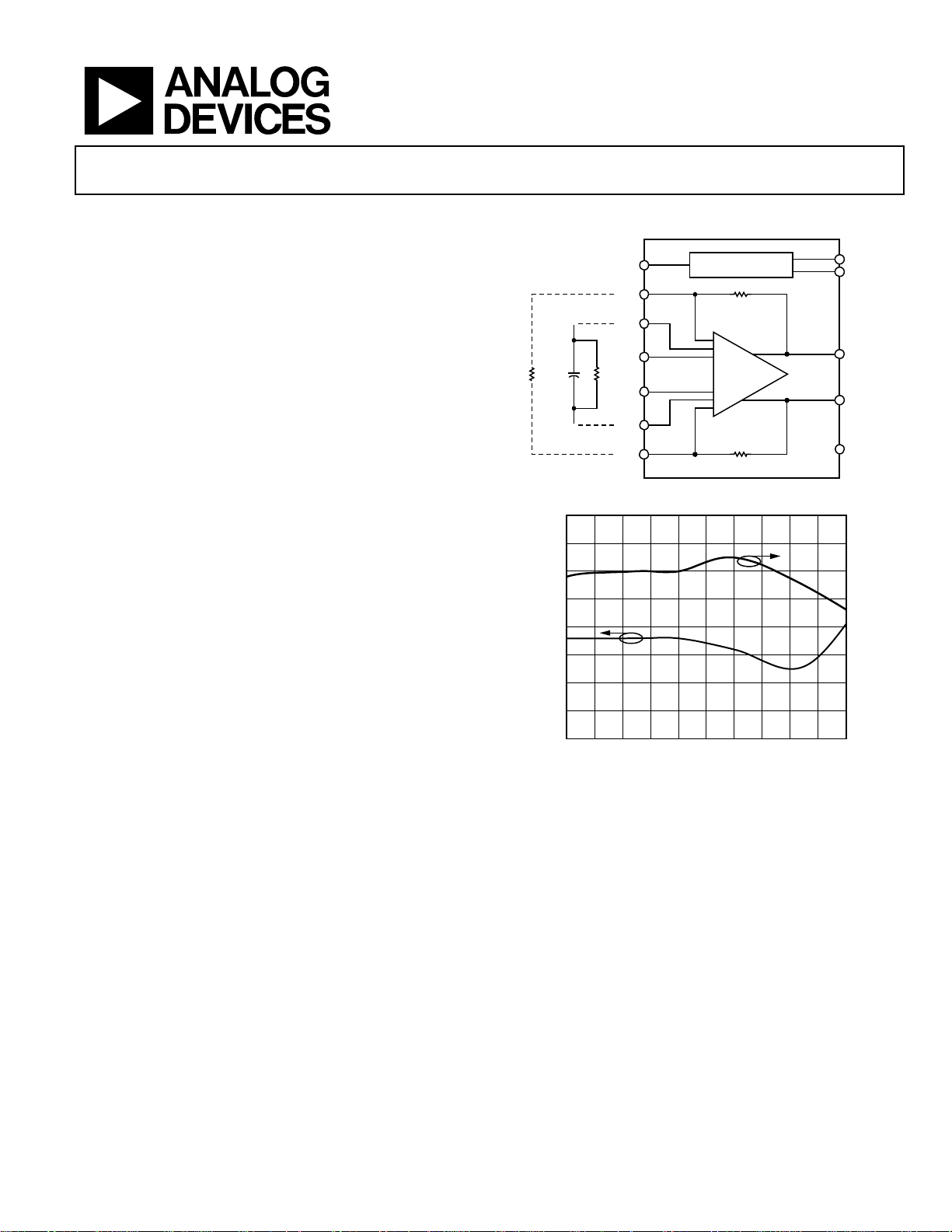
Differential RF/IF Amplifier
AD8352
FUNCTIONAL BLOCK DIAGRAM
ENB
RGP
RDP
C
D
R
G
60
–65
–70
–75
–80
HD3 (dBc)
–85
–90
VIP
R
D
VIN
RDN
RGN
BIAS CELL
+
–
AD8352
Figure 1.
VCM
VCC
VOP
VON
GND
5728-001
44
42
40
38
36
IP3 (dBm)
34
32
GENERAL DESCRIPTION
The AD8352 is a high performance differential amplifier
optimized for RF and IF applications. It achieves better than
80 dB SFDR performance at frequencies up to 200 MHz, and
65 dB beyond 500 MHz, making it an ideal driver for high
speed 12-bit to 16-bit analog-to-digital converters (ADCs).
Unlike other wideband differential amplifiers, the AD8352 has
buffers that isolate the gain setting resistor (R
inputs. As a result, the AD8352 maintains a constant 3 kΩ input
resistance for gains of 3 dB to 25 dB, easing matching and input
drive requirements. The AD8352 has a nominal 100 Ω differential
output resistance.
Rev. A
Information furnished by Analog Devices is believed to be accurate and reliable. However, no
responsibility is assumed by Anal og Devices for its use, nor for any infringements of patents or ot her
rights of third parties that may result from its use. Specifications subject to change without notice. No
license is granted by implication or otherwise under any patent or patent rights of Analog Devices.
Trademarks and registered trademarks are the property of their respective owners.
) from the signal
G
–95
–100
40 60 80 100 120 140 160 180 200
20 220
FREQUENCY (MHz)
Figure 2. IP3 and Third Harmonic Distortion vs. Frequency,
Measured Differentially
The device is optimized for wideband, low distortion performance at frequencies beyond 500 MHz. These attributes, together
with its wide gain adjust capability, make this device the amplifier
of choice for general-purpose IF and broadband applications
where low distortion, noise, and power are critical. In particular,
it is ideally suited for driving not only ADCs, but also mixers,
pin diode attenuators, SAW filters, and multielement discrete
devices. The device is available in a compact 3 mm × 3 mm,
16-lead LFCSP package and operates over a temperature range
of −40°C to +85°C.
One Technology Way, P.O. Box 9106, Norwood, MA 02062-9106, U.S.A.
Tel: 781.329.4700 www.analog.com
Fax: 781.461.3113 ©2006 Analog Devices, Inc. All rights reserved.
30
28
05728-002
Page 2

AD8352
TABLE OF CONTENTS
Features .............................................................................................. 1
Applications..................................................................................... 11
Applications....................................................................................... 1
Functional Block Diagram .............................................................. 1
General Description......................................................................... 1
Revision History ............................................................................... 2
Specifications..................................................................................... 3
Noise Distortion Specifications .................................................. 4
Absolute Maximum Ratings............................................................ 6
ESD Caution.................................................................................. 6
Pin Configuration and Function Descriptions............................. 7
Typical Performance Characteristics ............................................. 8
REVISION HISTORY
9/06—Rev. 0 to Rev. A
Changes to Absolute Maximum Ratings....................................... 6
Inserted Figure 10, Figure 11, and Figure 13 ................................ 9
Inserted Figure 17, Figure 18, and Figure 21 ..............................10
Changes to Figure 34...................................................................... 14
Changes to Table 9.......................................................................... 16
Changes to Figure 38...................................................................... 18
Changes to Ordering Guide.......................................................... 19
Gain and Distortion Adjustment (Differential Input) .......... 11
Single-Ended Input Operation ................................................. 12
Narrow-Band, Third-Order Intermodulation Cancellation.13
High Performance ADC Driving ............................................. 14
Layout and Transmission Line Effects..................................... 15
Evaluation Board ............................................................................ 16
Evaluation Board Loading Schemes ........................................ 16
Evaluation Board Schematics ................................................... 17
Outline Dimensions ....................................................................... 19
Ordering Guide .......................................................................... 19
1/06—Revision 0: Initial Version
Rev. A | Page 2 of 20
Page 3

AD8352
SPECIFICATIONS
VS = 5 V, RL = 200 Ω differential, RG = 118 Ω (AV = 10 dB), f = 100 MHz, T = 25°C; parameters specified differentially (in/out), unless
otherwise noted. C
Table 1.
Parameter Conditions Min Typ Max Unit
DYNAMIC PERFORMANCE
−3 dB Bandwidth AV = 6 dB, V
A
A
Bandwidth for 0.1 dB Flatness 3 dB ≤ AV ≤ 20 dB, V
Bandwidth for 0.2 dB Flatness 3 dB ≤ AV ≤ 20 dB, V
Gain Accuracy Using 1% resistor for RG, 0 dB ≤ AV ≤ 20 dB ±1 dB
Gain Supply Sensitivity VS ± 5% 0.06 dB/V
Gain Temperature Sensitivity −40°C to +85°C 4 mdB/°C
Slew Rate RL = 1 kΩ, V
R
Settling Time 2 V step to 1% <2 ns
Overdrive Recovery Time VIN = 4 V to 0 V step, V
Reverse Isolation (S12) −80 dB
INPUT/OUTPUT CHARACTERISTICS
Common-Mode Nominal VCC/2 V
Voltage Adjustment Range 1.2 to 3.8 V
Maximum Output Voltage Swing 1 dB compressed 6 V p-p
Output Common-Mode Offset Referenced to VCC/2 −100 +20 mV
Output Common-Mode Drift −40°C to +85°C 0.25 mV/°C
Output Differential Offset Voltage −20 +20 mV
CMRR 57 dB
Output Differential Offset Drift −40°C to +85°C 0.15 mV/°C
Input Bias Current ±5 μA
Input Resistance 3 kΩ
Input Capacitance (Single-Ended) 0.9 pF
Output Resistance 100 Ω
Output Capacitance 3 pF
POWER INTERFACE
Supply Voltage 3 5 5.5 V
ENB Threshold 1.5 V
ENB Input Bias Current ENB at 3 V 75 nA
ENB at 0.6 V −125 μA
Quiescent Current ENB at 3 V 35 37 39 mA
ENB at 0.6 V 5.3 mA
and RD are selected for differential broadband operation (see Tabl e 5 and Ta b le 6 ).
D
≤ 1.0 V p-p 2500 MHz
OUT
= 10 dB, V
V
= 14 dB, V
V
= 200 Ω, V
L
≤ 1.0 V p-p 2200 MHz
OUT
≤ 1.0 V p-p 1800 MHz
OUT
≤ 1.0 V p-p 190 MHz
OUT
≤ 1.0 V p-p 300 MHz
OUT
= 2 V step 9 V/ns
OUT
= 2 V step 8 V/ns
OUT
≤ ±10 mV <3 ns
OUT
Rev. A | Page 3 of 20
Page 4

AD8352
NOISE DISTORTION SPECIFICATIONS
VS = 5 V, RL = 200 Ω differential, RG = 118 Ω (AV = 10 dB), V
otherwise noted. C
and RD are selected for differential broadband operation (see Tabl e 5 and Ta b le 6 ). See the Applications section for
D
single-ended to differential performance characteristics.
Table 2.
Parameter Conditions Min Typ Max Unit
10 MHz
Second/Third Harmonic Distortion
R
1
RL = 1 kΩ, V
= 200 Ω, V
L
OUT
OUT
Output Third-Order Intercept RL = 200 Ω, f1 = 9.5 MHz, f2 = 10.5 MHz +38 dBm
Third-Order IMD
= 1 kΩ, f1 = 9.5 MHz, f2 = 10.5 MHz,
R
L
= 2 V p-p composite
V
OUT
= 200 Ω, f1 = 9.5 MHz, f2 = 10.5 MHz,
R
L
= 2 V p-p composite
V
OUT
Noise Spectral Density (RTI) +2.7 nV/√Hz
1 dB Compression Point (RTO) +15.7 dBm
70 MHz
Second/Third Harmonic Distortion RL = 1 kΩ, RG = 178 Ω, V
R
= 200 Ω, RG = 115 Ω, V
L
Output Third-Order Intercept RL = 200 Ω f1 = 69.5 MHz, f2 = 70.5 MHz +40 dBm
Third-Order IMD
= 1 kΩ, f1 = 69.5 MHz, f2 = 70.5 MHz,
R
L
= 2 V p-p composite
V
OUT
= 200 Ω, f1 = 69.5 MHz, f2 = 70.5 MHz,
R
L
V
= 2 V p-p composite
OUT
Noise Spectral Density (RTI) +2.7 nV/√Hz
1 dB Compression Point (RTO) +15.7 dBm
100 MHz
Second/Third Harmonic Distortion RL = 1 kΩ, V
R
= 200 Ω, V
L
OUT
OUT
Output Third-Order Intercept RL = 200 Ω, f1 = 99.5 MHz, f2 = 100.5 MHz +40 dBm
Third-Order IMD
= 1 kΩ, f1 = 99.5 MHz, f2 = 100.5 MHz,
R
L
= 2 V p-p composite
V
OUT
= 200 Ω, f1 = 99.5 MHz, f2 = 100.5 MHz,
R
L
= 2 V p-p composite
V
OUT
Noise Spectral Density (RTI) +2.7 nV/√Hz
1 dB Compression Point (RTO) +15.6 dBm
140 MHz
Second/Third Harmonic Distortion RL = 1 kΩ, V
R
= 200 Ω, V
L
OUT
OUT
Output Third-Order Intercept RL = 200 Ω, f1 = 139.5 MHz, f2 = 140.5 MHz +41 dBm
Third-Order IMD
= 1 kΩ, f1 = 139.5 MHz, f2 = 140.5 MHz,
R
L
= 2 V p-p composite
V
OUT
= 200 Ω, f1 = 139.5 MHz, f2 = 140.5 MHz,
R
L
V
= 2 V p-p composite
OUT
Noise Spectral Density (RTI) +2.7 nV/√Hz
1 dB Compression Point (RTO) +15.5 dBm
= 2 V p-p composite, T = 25°C; parameters specified differentially, unless
OUT
= 2 V p-p −88/−95 dBc
= 2 V p-p −86/−82 dBc
−86 dBc
−81 dBc
= 2 V p-p −83/−84 dBc
OUT
= 2 V p-p −84/−82 dBc
OUT
−91 dBc
−83 dBc
= 2 V p-p −83/−83 dBc
= 2 V p-p −84/−82 dBc
−91 dBc
−84 dBc
= 2 V p-p −83/−82 dBc
= 2 V p-p −82/−84 dBc
−89 dBc
−85 dBc
Rev. A | Page 4 of 20
Page 5

AD8352
Parameter Conditions Min Typ Max Unit
190 MHz
Second/Third Harmonic Distortion RL = 1 kΩ, V
R
= 200 Ω, V
L
Output Third-Order Intercept RL = 200 Ω, f1 = 180.5 MHz, f2 = 190.5 MHz +39 dBm
Third-Order IMD
= 1 kΩ, f1 = 180.5 MHz, f2 = 190.5 MHz,
R
L
= 2 V p-p composite
V
OUT
= 200 Ω, f1 = 180.5 MHz, f2 = 190.5 MHz,
R
L
V
= 2 V p-p composite
OUT
Noise Spectral Density (RTI) +2.7 nV/√Hz
1 dB Compression Point (RTO) +15.4 dBm
240 MHz
Second/Third Harmonic Distortion RL = 1 kΩ, V
R
= 200 Ω, V
L
Output Third-Order Intercept RL = 200 Ω, f1 = 239.5 MHz, f2 = 240.5 MHz +36 dBm
Third-Order IMD
= 1 kΩ, f1 = 239.5 MHz, f2 = 240.5 MHz,
R
L
V
= 2 V p-p composite
OUT
= 200 Ω, f1 = 239.5 MHz, f2 = 240.5 MHz,
R
L
= 2 V p-p composite
V
OUT
Noise Spectral Density (RTI) +2.7 nV/√Hz
1 dB Compression Point (RTO) +15.3 dBm
380 MHz
Second/Third Harmonic Distortion
R
2
RL = 1 kΩ, V
= 200 Ω, V
L
Output Third-Order Intercept RL = 200 Ω, f1 = 379.5 MHz, f2 = 380.5 MHz +33 dBm
Third-Order IMD
= 1 kΩ, f1 = 379.5 MHz, f2 = 380.5 MHz,
R
L
= 2 V p-p composite
V
OUT
= 200 Ω, f1 = 379.5 MHz, f2 = 380.5 MHz,
R
L
V
= 2 V p-p composite
OUT
Noise Spectral Density (RTI) +2.7 nV/√Hz
1 dB Compression Point (RTO) +14.6 dBm
500 MHz
Second/Third Harmonic Distortion RL = 200 Ω, V
Output Third-Order Intercept RL = 200 Ω, f1 = 499.5 MHz, f2 = 500.5 MHz +28 dBm
Third-Order IMD
= 200 Ω, f1 = 499.5 MHz, f2 = 500.5 MHz,
R
L
V
= 2 V p-p composite
OUT
Noise Spectral Density (RTI) +2.7 nV/√Hz
1 dB Compression Point (RTO) +13.9 dBm
1
When using the evaluation board at frequencies below 50 MHz, replace the Output Balun T1 with a transformer such as Mini-Circuits® ADT1-1WT to obtain the low
frequency balance required for differential HD2 cancellation.
2
CD and RD can be optimized for broadband operation below 180 MHz. For operation above 300 MHz, CD and RD components are not required.
= 2 V p-p −82/−85 dBc
OUT
= 2 V p-p −81/−87 dBc
OUT
−83 dBc
−81 dBc
= 2 V p-p −82/−76 dBc
OUT
= 2 V p-p −80/−73 dBc
OUT
−85 dBc
−77 dBc
= 2 V p-p −72/−68 dBc
OUT
= 2 V p-p −74/−69 dBc
OUT
−74 dBc
−70 dBc
= 2 V p-p −71/−64 dBc
OUT
−61 dBc
Rev. A | Page 5 of 20
Page 6
AD8352
ABSOLUTE MAXIMUM RATINGS
Table 3.
Parameter Rating
Supply Voltage VCC 5.5 V
VIP, VIN VCC + 0.5 V
Internal Power Dissipation 210 mW
θ
JA
Maximum Junction Temperature 125°C
Operating Temperature Range −40°C to +85°C
Storage Temperature Range −65°C to +150°C
Lead Temperature (Soldering 60 sec) 300°C
91.4°C/W
Stresses above those listed under Absolute Maximum Ratings
may cause permanent damage to the device. This is a stress
rating only; functional operation of the device at these or any
other conditions above those indicated in the operational
section of this specification is not implied. Exposure to absolute
maximum rating conditions for extended periods may affect
device reliability.
ESD CAUTION
Rev. A | Page 6 of 20
Page 7

AD8352
PIN CONFIGURATION AND FUNCTION DESCRIPTIONS
ENB
VIP
VCM
VCC
14
13
15
16
PIN 1
INDICATOR
1RDP
2RGP
AD8352
3RGN
TOP VIEW
(Not to Scale)
4RDN
5
6
VIN
GND
Figure 3. Pin Configuration
Table 4. Pin Function Descriptions
Pin No. Mnemonic Description
1 RDP Positive Distortion Adjust.
2 RGP Positive Gain Adjust.
3 RGN Negative Gain Adjust.
4 RDN Negative Distortion Adjust.
5 VIN Balanced Differential Input. Biased to VCM, typically ac-coupled.
6, 7, 9, 12 GND Ground. Connect to low impedance GND.
8, 13 VCC Positive Supply.
10 VON Balanced Differential Output. Biased to VCM, typically ac-coupled.
11 VOP Balanced Differential Output. Biased to VCM, typically ac-coupled.
14 VCM
Common-Mode Voltage. A voltage applied to this pin sets the common-mode voltage of the input and output.
Typically decoupled to ground with a 0.1 μF capacitor. With no reference applied, input and output common
mode floats to midsupply (VCC/2).
15 ENB Enable. Apply positive voltage (1.3 V < ENB < VCC) to activate device.
16 VIP Balanced Differential Input. Biased to VCM, typically ac-coupled.
12 GND
11 VOP
10 VON
9GND
8
7
VCC
GND
05728-003
Rev. A | Page 7 of 20
Page 8

AD8352
TYPICAL PERFORMANCE CHARACTERISTICS
25
20
15
10
GAIN (dB)
5
0
RG=43Ω
RG= 100Ω
RG= 520Ω
30
25
RG=20Ω
20
RG= 100Ω
15
RG= 182Ω
10
GAIN (dB)
RG= 383Ω
5
RG= 715Ω
0
–5
10 10k
100 1k
FREQUENCY (MHz)
Figure 4. Gain vs. Frequency for a 200 Ω Differential Load with Baluns,
A
= 18 dB, 12 dB, and 6 dB
V
25
20
15
10
GAIN (dB)
5
0
–5
10 10k
RG=62Ω
RG= 190Ω
RG=3kΩ
100 1k
FREQUENCY (MHz)
Figure 5. Gain vs. Frequency for a 1 kΩ Differential Load with Baluns,
A
= 18 dB, 12 dB, and 6 dB
V
25
RG=19Ω
20
RG=64Ω
15
RG= 118Ω
10
GAIN (dB)
RG= 232Ω
5
RG= 392Ω
0
–5
10 10k
05728-036
100 1k
FREQUENCY (MHz)
05728-039
Figure 7. Gain vs. Frequency for a 1 kΩ Differential Load Without Baluns,
R
Open, AV = 25 dB, 14 dB, 10 dB, 6 dB, and 3 dB
D/CD
13.0
12.5
12.0
11.5
11.0
10.5
GAIN (dB)
10.0
9.5
RL= 200Ω
9.0
= 118Ω
R
G
=0.004dBc
T
C
8.5
8.0
10 10k
05728-037
–40°C
+85°C
+25°C
–40°C
+85°C
+25°C
100 1k
FREQUENCY (MHz)
RL=1kΩ
= 182Ω
R
G
= 0.002dB/°C
T
C
11. 0
10.5
10.0
9.5
9.0
8.5
8.0
7.5
7.0
6.5
6.0
GAIN (dB)
05728-040
Figure 8. Gain vs. Frequency over Temperature (−40°C, +25°C, +85°C)
Without Baluns, A
80
70
RL=200Ω
60
RL=1kΩ
50
40
CMRR (dB)
30
20
= 10 dB, RL = 200 Ω and 1 kΩ
V
–5
10 10k
100 1k
FREQUENCY (MHz)
Figure 6. Gain vs. Frequency for a 200 Ω Differential Load Without Baluns,
Open, AV = 22 dB, 14 dB, 10 dB, 6 dB, and 3 dB
R
D/CD
Rev. A | Page 8 of 20
10
10 1000
05728-038
Figure 9. CMRR vs. Frequency, R
100
FREQUENCY (MHz)
= 200 Ω and 1 kΩ,
L
05728-043
Differential Source Resistance
Page 9

AD8352
50
45
OIP3
40
35
30
25
AV= 10dB
20
NOISE FI GURE (dB), IP3 (dBm)
NOISE FI GURE
15
10
0 50 100 150 200 250 300 350 400 450 500
AV= 6dB
AV= 10dB
FREQUENCY (M Hz)
AV= 10dB
AV= 15dB
Figure 10. Noise Figure, OIP3, and Spectral Noise Density vs. Frequency,
2 V p-p Composite, R
= 200 Ω
L
5.0
4.5
4.0
3.5
3.0
2.5
2.0
1.5
1.0
16.5
16.0
15.5
15.0
14.5
OUTPUT P1dB (dBm)
14.0
SPECTRAL NOISE DENSITY RTI (nV/ Hz)
05728-049
13.5
13.0
70MHz
380MHz
500MHz
0 10050 200 300150 250 350 450400
GAIN SETTING RESISTOR (Ω)
100MHz
240MHz
140MHz
190MHz
05728-051
Figure 13. Output 1 dB Compression Point vs. RG
for Multiple Frequencies, R
= 200 Ω
L
45
40
35
OIP3 (dBm)
30
25
20
0 10050 200 300150 250 350 400
70MHz
Figure 11. Output IP3 vs. R
–60
–65
–70
–75
HD3
2V p-p
140MHz
240MHz
380MHz
500MHz
GAIN SETTING RESISTOR (Ω)
for Multiple Frequencies, RL = 200 Ω
G
> 300MHz NO CD OR RDUSED
HD2
2V p-p
100MHz
190MHz
–60
–65
–70
–75
–80
–85
–90
–95
HARMONIC DISTORTION ( dBc)
–100
–105
05728-050
–110
0 500
50 100 150 200 250 300 350 400 450
FREQUENCY (MHz)
Figure 14. Harmonic Distortion vs. Frequency for 2 V p-p into R
= 10 dB, 5 V Supply, RG = 180 Ω, RD = 6.8 kΩ, CD = 0.1 pF
A
V
–50
–60
–70
–80
HD3
HD2
HD3
HD2
= 1 kΩ,
L
05728-005
–80
HARMONIC DISTORTION ( dBc)
–85
–90
220 260 300 340 380 420 460 500
HD3
1V p-p
FREQUENCY (MHz)
Figure 12. Third-Order Harmonic Distortion HD3 vs. Frequency,
A
= 10 dB, RL = 200 Ω
V
05728-009
Rev. A | Page 9 of 20
–90
HARMONIC DISTORTION ( dBc)
–100
–110
0 400
50 100 150 200 250 300 350
FREQUENCY (MHz)
Figure 15. Harmonic Distortion vs. Frequency for 2 V p-p into R
= 10 dB, RG = 115 Ω, RD = 4.3 kΩ, CD = 0.2 pF
A
V
= 200 Ω,
L
05728-007
Page 10

AD8352
0.6
0.5
0.4
0.3
0.2
GROUP DELAY (ns)
0.1
0
01000
100 200 300 400 500 600 700 800 900
FREQUENCY (MHz)
Figure 16. Phase and Group Delay vs. Frequency, A
3500
3000
2500
2000
1500
1000
INPUT RESISTANCE (Ω)
500
0
0 100 200 300 1000400 500 600 700 800 900
FREQUENCY (MHz )
Figure 17. S11 Equivalent RC Parallel Network R
0
–20
–40
–60
–80
–100
–120
= 10 dB, RL = 200 Ω
V
0
–0.05
–0.10
–0.15
–0.20
–0.25
–0.30
–0.35
= 115 Ω
G
PHASE (Degrees)
05728-042
INPUT CAPACIT ANCE (pF)
05728-052
1.5
1.0
0.5
0
VOLTAGE (V)
–0.5
–1.0
–1.5
0.5 1.0 1.5 2.0 2.5
03.0
TIME (nsec)
Figure 19. Large Signal Output Transient Response, R
5
4
3
2
1
0
–1
SETTLING (%)
–2
–3
–4
–5
04
0.5 1.0 1.5 2.0 2.5 3.0 3.5
TIME (nsec)
T
(10/90) = 215psec
RISE
T
(10/90) = 210psec
FALL
= 200 Ω, AV = 10 dB
L
05728-046
.0
05728-047
Figure 20. 1% Settling Time for a 2 V p-p Step Response,
= 10 dB, RL = 200 Ω
A
V
160
140
120
100
80
60
OUTPUT RESI STANCE (Ω)
40
20
0
0 100 20 0 300 1000400 500 600 700 800 900
FREQUENCY (MHz)
Figure 18. S22 Equivalent RC Parallel Network RG = 115 Ω
0.7
0.6
0.5
0.4
0.3
0.2
0.1
OUTPUT CAPACIT ANCE (pF)
0
–1.0
05728-053
Rev. A | Page 10 of 20
6
5
4
3
2
1
SPECTRAL NOISE DENSITY RTI (nV/ Hz)
0
0 50 100 150 400200 250 300 350
GAIN SETTING RESISTOR (Ω)
Figure 21. Noise Figure and Noise Spectral Density RTI vs. R
= 200 Ω
R
L
25
20
15
10
NOISE FIGURE (dB)
5
0
05728-054
,
G
Page 11
AD8352
APPLICATIONS
GAIN AND DISTORTION ADJUSTMENT (DIFFERENTIAL INPUT)
Tabl e 5 and Ta b le 6 show the required value of RG for the gains
specified at 200 Ω and 1 kΩ loads.
gain vs. R
output loads (R
up to 18 dB for both load conditions. For other
G
), use Equation 1 to compute gain vs. RG.
L
⎛
⎜
A
=
ialVDifferent
⎜
G
⎝
where:
R
= single-ended load.
L
R
= gain setting resistor.
G
The third-order harmonic distortion can be reduced by using
external components R
required values for R
and CD. Tabl e 5 and Ta b le 6 show the
D
and CD for the specified gains to achieve
D
(single tone) third-order distortion reduction at 180 MHz.
Figure 23 and Figure 25 show any gain (up to 18 dB) vs. CD for
200 Ω and 1 kΩ loads, respectively. When these values are
selected, they result in minimum single tone, third-order
distortion at 180 MHz. This frequency point provides the best
overall broadband distortion for the specified frequencies below
and above this value. For applications above approximately
300 MHz, C
and RD are not required. See the Specifications
D
section and third-order harmonic plots in the
Performance Characteristics
can be further optimized for narrow-band tuning require-
C
D
ments below 180 MHz that result in relatively lower third-order
(in-band) intermodulation distortion terms. See the
Band, Third-Order Intermodulation Cancellation
more information. Though not shown, single tone, third-order
optimization can also be improved for narrow-band frequency
applications below 180 MHz with the proper selection of C
and 3 dB to 6 dB of relative third-order improvement can be
realized at frequencies below approximately 140 MHz.
Using the information listed in
value for R
can be determined for loads between 200 Ω and 1 kΩ.
D
For loads above 1 kΩ, use the 1 kΩ R
Table 5. Broadband Selection of R
AV (dB) RG (Ω) CD (pF) RD (kΩ)
3 390 Open 6.8
6 220 Open 4.3
9 140 0.1 4.3
10 115 0.2 4.3
12 86 0.3 4.3
15 56 0.6 4.3
18 35 1 4.3
Figure 22 and Figure 24 plot
+
500
R
G
RR
L
⎞
⎟
(1)
R
L
⎟
+++
430)53()5(
⎠
Ty pi ca l
section for more details.
Narrow-
section for
Tabl e 5 and Ta bl e 6, an extrapolated
values listed in Tabl e 6.
D
, CD, and RD: 200 Ω Load
G
,
D
Table 6. Broadband Selection of RG, CD, and RD: 1 kΩ Load
AV (dB) RG (Ω) CD (pF) RD (kΩ)
3 750 Open 6.8
6 360 Open 6.8
9 210 Open 6.8
10 180 0.05 6.8
12 130 0.1 6.8
15 82 0.3 6.8
18 54 0.5 6.8
20
18
16
14
12
10
GAIN (dB)
8
6
4
2
0
0 400
100 200 30050 150 250 350
R
(Ω)
G
Figure 22. Gain vs. R
, RL = 200 Ω
G
05728-026
20
18
16
14
12
10
GAIN (dB)
8
6
4
2
0
0
0.2 0. 4 0.6 0.8 1.00.1 0. 3 0.5 0.7 0.9
C
(pF)
D
Figure 23. Gain vs. C
, RL = 200 Ω
D
05728-027
Rev. A | Page 11 of 20
Page 12

AD8352
A
–
20
18
16
14
12
10
GAIN (dB)
8
6
4
2
0
0 800
100 200 300 400 500 600 700
R
(Ω)
G
Figure 24. Gain vs. R
20
18
16
14
12
10
GAIN (dB)
8
6
4
2
0
00
0.1 0. 2 0.3 0.4
Figure 25. Gain vs. C
C
D
, RL = 1 kΩ
G
(pF)
, RL = 1 kΩ
D
05728-028
.5
05728-029
SINGLE-ENDED INPUT OPERATION
The AD8352 can be configured as a single-ended to differential
amplifier as shown in
driving only the VIP input, an external resistor (R
added between VIP and RGN. See Equation 2 to determine the
single-ended input gain (A
A
−
endedVSingle
where:
= single-ended load.
R
L
= gain setting resistor.
R
G
Figure 27 plots gain vs. RG for 200 Ω and 1 kΩ loads. Table 7
Tabl e 8 show the values of CD and RD required (for 180 MHz
and
broadband, third-order, single tone optimization) for 200 Ω and
1 kΩ loads, respectively. This single-ended configuration provides
−3 dB bandwidths similar to input differential drive.
through
Figure 30 show distortion levels at a gain of 12 dB for
both 200 Ω and 1 kΩ loads. Gains from 3 dB to 18 dB, using
optimized C
and RD values, obtain similar distortion levels.
D
Figure 26. To balance the outputs when
N
VSingl e-ended
⎛
⎜
=
⎜
G
⎝
) for a given RG or RL.
+
500
R
G
+++
RR
L
430)53()5(
⎞
⎟
R
L
⎟
⎠
) of 200 Ω is
R
L
+
+
30
R
L
Figure 28
(2)
50Ω
C
65Ω
25Ω
0.1µF
0.1µF
RDR
C
D
R
N
200Ω
VIP
RGP
G
AD8352
RGN
Figure 26. Single-Ended Schematic
40
35
30
25
20
GAIN (dB)
15
10
5
0
1
60
–70
–80
(dBc)
–90
–100
–110
GAIN, RL=200Ω
10 100 1k
2NDS, 2V p-p OUT
10 70 140 190 240
GAIN, RL=1kΩ
R
(Ω)
G
Figure 27. Gain vs. R
2NDS, 1V p-p OUT
FREQUENCY (MHz)
G
Figure 28. Single-Ended,
Second-Order Harmonic Distortion, 200 Ω Load
This broadband optimization was also performed at 180 MHz.
As with differential input drive, the resulting distortion levels
at lower frequencies are based on the C
and RD specified in
D
Tabl e 7 and Ta b le 8 . As with differential input drive, relative
third-order reduction improvement at frequencies below
140 MHz are realized with proper selection of C
0.1µF
0.1µF
and RD.
D
10k
05728-024
05728-020
05728-021
Rev. A | Page 12 of 20
Page 13

AD8352
–
–
–
60
–70
3RDS, 2V p-p OUT
–80
(dBc)
–90
–100
–110
10 70 140 190 240
3RDS, 1V p- p OUT
FREQUENCY (MHz)
Figure 29. Single-Ended, Third-Order Harmonic Distortion, 200 Ω Load
60
–70
–80
(dBc)
–90
–100
2NDS, 2V p- p OUT
2NDS, 1V p-p OUT
Table 8. Distortion Cancellation Selection Components
(R
and CD) for Required Gain, 1 kΩ Load
D
AV (dB) RG (Ω) CD (pF) RD (kΩ)
6 3 k Open 4.3
9 470 Open 4.3
12 210 0.2 4.3
15 120 0.3 4.3
18 68 0.5 4.3
NARROW-BAND, THIRD-ORDER INTERMODULATION CANCELLATION
Broadband, single tone, third-order harmonic optimization
05728-022
does not necessarily result in optimum (minimum) two tone,
third-order intermodulation levels. The specified values for C
and R
in Tabl e 5 and Tabl e 6 were determined for minimizing
D
D
broadband, single tone, third-order levels.
Due to phase-related distortion coefficients, optimizing single
tone, third-order distortion does not result in optimum in band
(2f
− f2 and 2f2 − f1), third-order distortion levels. By proper
1
selection of C
(using a fixed 4.3 kΩ RD), IP3s of better than
D
45 dBm are achieved. This results in degraded out-of-band,
third-order frequencies (f
+ 2f1, f1 + 2f2, 3f1 and 3f2). Thus,
2
careful frequency planning is required to determine the
tradeoffs.
–110
10 70 140 190 240
FREQUENCY (MHz)
05728-023
Figure 30. Single-Ended, Second-Order Harmonic Distortion, 1 kΩ Load
60
–70
–80
(dBc)
–90
–100
–110
3RDS, 2V p- p OUT
3RDS, 1V p- p OUT
10 70 140 190 240
FREQUENCY (MHz)
05728-025
Figure 31. Single-Ended, Third-Order Harmonic Distortion, 1 kΩ Load
Table 7. Distortion Cancellation Selection Components
(R
and CD) for Required Gain, 200 Ω Load
D
AV (dB) RG (Ω) CD (pF) RD (kΩ)
3 4.3 k Open 4.3
6 540 Open 4.3
9 220 0.1 4.3
12 120 0.3 4.3
15 68 0.6 4.3
18 43 0.9 4.3
Rev. A | Page 13 of 20
Figure 32 shows narrow band (2 MHz spacing) OIP3 levels
optimized at 32 MHz, 70 MHz, 100 MHz, and 180 MHz using
the C
values specified in Figure 33. These four data points (the
D
C
value and associated IP3 levels) are extrapolated to provide
D
close estimates of IP3 levels for any specific frequency between
30 MHz and 180 MHz. For frequencies below approximately
140 MHz, narrow-band tuning of IP3 results in relatively higher
IP3s (vs. the broadband results shown in
Tabl e 2 specifications).
Though not shown, frequencies below 30 MHz also result in
improved IP3s when using proper values for C
48
47
46
45
44
6dB
=
A
43
OIP3 (dBm)
42
41
40
39
38
02
Figure 32. Third-Order Intermodulation Distortion vs. Frequency for
V
10dB
15dB
18dB
50 100 150
FREQUENCY (MHz)
Various Gain Settings
.
D
RL = 200Ω
R
= 4.3kΩ
D
C
= 0.3pF
D
00
05728-030
Page 14

AD8352
V
A
6.0
5.5
5.0
4.5
4.0
3.5
3.0
(pF)
D
C
2.5
2.0
1.5
1.0
0.5
0
30 190
50 70 90 110 130 150 170
Figure 33. Narrow-Band C
D
6dB
=
A
V
10dB
15dB
18dB
FREQUENCY (MHz)
vs. Frequency for Various Gain Settings
HIGH PERFORMANCE ADC DRIVING
The AD8352 provides the gain, isolation, and balanced low
distortion output levels for efficiently driving wideband ADCs
such as the
Figure 34 and Figure 35 (single and differential input drive)
illustrate the typical front-end circuit interface for the AD8352
differentially driving the AD9445 14-bit ADC at 105 MSPS. The
AD8352, when used in the single-ended configuration, shows
little or no degradation in overall third-order harmonic performance (vs. differential drive). See the
Operation
and
Though not shown, the single-ended, third-order levels are similar.
The 50 Ω resistor shown in
input impedance to the source for matching considerations.
When the driver is less than one eighth of the wavelength from
the AD8352, impedance matching is not required thereby
negating the need for this termination resistor. The output 24 Ω
resistors provide isolation from the analog-to-digital input.
Refer to the
more information. The circuit in
ended input to differential output configuration for driving the
AD9445. In this case, the input 50 Ω resistor with R
200 Ω) provide the input impedance match for a 50 Ω system.
Again, if input reflections are minimal, this impedance match is
not required. A fixed 200 Ω resistor (R
the output voltages that are required for second-order distortion
cancellation. R
the R
The AD9445 presents approximately 2 kΩ in parallel with
5 pF/differential load to the AD8352 and requires a 2.0 V p-p
differential signal (V
full-scale output operation.
AD9445.
section. The 100 MHz FFT plots shown in Figure 36
Figure 37 display the results for the differential configuration.
Figure 34 provides a 50 Ω differential
Layout and Transmission Line Effects section for
Figure 35 represents a single-
) is required to balance
N
is the gain setting resistor for the AD8352 with
G
and CD components providing distortion cancellation.
D
= 1 V) between VIN+ and VIN− for a
REF
RL = 200Ω
R
= 4.3kΩ
D
Single-Ended Input
(typically
N
These AD8352 simplified circuits provide the gain, isolation,
and distortion performance necessary for efficiently driving
high linearity converters such as the AD9445. This device also
provides balanced outputs whether driven differentially or
single-ended, thereby maintaining excellent second-order
distortion levels. However, at frequencies above approximately
100 MHz, due to phase related errors, single-ended, secondorder distortion is relatively higher. The output of the amplifier
is ac-coupled to allow for an optimum common-mode setting at
the ADC input. Input ac coupling can be required if the source
also requires a common-mode voltage that is outside the optimum range of the AD8352. A VCM common-mode pin is
provided on the AD8352 that equally shifts both input and
05728-031
output common-mode levels. Increasing the gain of the AD8352
increases the system noise and, thus, decreases the SNR (3.5 dB
at 100 MHz input for Av = 10 dB) of the AD9445 when no
filtering is used. Note that amplifier gains from 3 dB to 18 dB,
with proper selection of C
and RD, do not appreciably affect
D
distortion levels. These circuits, when configured properly, can
result in SFDR performance of better than 87 dBc at 70 MHz
and 82 dBc at 180 MHz input. Single-ended drive, with appropriate
C
and RD, give similar results for SFDR and third-order
D
intermodulation levels shown in these figures.
Placing antialiasing filters between the ADC and the amplifier
is a common approach for improving overall noise and broadband
distortion performance for both band-pass and low-pass applications. For high frequency filtering, matching to the filter is
required. The AD8352 maintains a 100 Ω output impedance
well beyond most applications and is well-suited to drive most
filter configurations with little or no degradation in distortion.
CC
0.1µF
0Ω
16
RDR
0Ω
1
2
G
3
4
5
IF/RF INPUT
ADT1-1WT
50Ω
C
D
0.1µF
Figure 34. Differential Input to the AD8352 Driving the AD9445
50Ω
C
25Ω
50Ω
0.1µF
0.1µF
RDR
C
D
200Ω
VIP
G
VIN
R
N
Figure 35. Single-Ended Input to the AD8352 Driving the AD9445
8, 13
AD8352
14
0.1µF
VOP
AD8352
VON
0.1µF
11
10
0.1µF
0.1µF
0.1µF
0.1µF
33Ω
33Ω
24Ω
24Ω
AD9445
VIN+
AD9445
VIN–
5728-012
05728-033
Rev. A | Page 14 of 20
Page 15

AD8352
0
–10
–20
–30
–40
–50
–60
–70
–80
(dBFS)
–90
–100
–110
–120
–130
–140
–150
0
5.25 10.50 15.75 21.00 26.25 31.50 36.75 42.00 47.25
FREQUENCY (MHz)
Figure 36. Single Tone Distortion AD8352 Driving AD9445
Encode Clock @ 105 MHz with Fc @ 100 MHz (A
0
–10
–20
–30
–40
–50
–60
–70
–80
(dBFS)
–90
–100
–110
–120
–130
–140
–150
0
5.25 10.50 15.75 21.00 26.25 31.50 36. 75 42.00 47.25
FREQUENCY (MHz)
Figure 37. Two Tone Distortion AD8352 Driving AD9445,
Encode Clock @ 105 MHz with Fc @ 100 MHz (A
Analog In = 98 MHz and 101 MHz, See
SNR = 67.26dBc
SFDR = 83.18dBc
NOISE FLOOR = –110.5dB
FUND = –1.074dBFS
SECOND = –83.14dBc
THIRD = –85.39dBc
= 10 dB), See Figure 34
V
SNR = 61.98dBc
NOISE FLOOR = –111.2dB
FUND1 = –7.072dBF S
FUND2 = –7.043dBF S
IMD (2F2-F 1) = –89dBc
IMD (2F1-F 2) = –88dBc
= 10 dB),
V
Figure 34
LAYOUT AND TRANSMISSION LINE EFFECTS
High Q inductive drives and loads, as well as stray transmission
line capacitance in combination with package parasitics, can
potentially form a resonant circuit at high frequencies resulting
in excessive gain peaking or possible oscillation. If RF transmission lines connecting the input or output are used, they should
be designed such that stray capacitance at the I/O pins is
minimized. In many board designs, the signal trace widths
should be minimal where the driver/receiver is less than oneeighth of the wavelength from the AD8352. This nontransmission
line configuration requires that underlying and adjacent ground
52.50
05728-034
,
52.50
05728-035
and low impedance planes be far removed from the signal lines.
In a similar fashion, stray capacitance should be minimized
near the R
, CD, and RD components and associated traces. This
G
also requires not placing low impedance planes near these
components. Refer to the evaluation board layout (
Figure 40) for more information. Excessive stray capacitance
and
at these nodes results in unwanted high frequency distortion.
The 0.1 μF supply decoupling capacitors need to be close to the
amplifier. This includes Signal Capacitor C2 through Signal
Capacitor C5.
Parasitic suppressing resistors (R5, R6, R7, and R11) can be
used at the device I/O pins. Use 25 Ω series resistors (Size 0402)
to adequately de-Q the input and output system from most
parasitics without a significant decrease in gain. In general, if
proper board layout techniques are used, the suppression
resistors are not necessarily required. Output Parasitic Suppression
Resistor R7 and Output Parasitic Suppression Resistor R11 can
be required for driving some switch cap ADCs. These suppressors,
with Input C of the converter (and possibly added External
Shunt C), help provide charge kickback isolation and improve
overall distortion at high encode rates.
Figure 39
Rev. A | Page 15 of 20
Page 16

AD8352
EVALUATION BOARD
An evaluation board is available for experimentation of various parameters such as gain, common-mode level, and distortion. The output
network can be configured for different loads via minor output component changes. The schematic and evaluation board artwork are
presented in
Table 9. Evaluation Board Circuit Components and Functions
Component Name Function Additional Information
C8, C9 Capacitors C8 and C9 are bypass capacitors. C8 = 0.1 μF, C9 = 0.1 μF
RD, C
D
R1, R2, R3, R4,
R5, R6, T2, C2,
C3
R7, R8, R9, R11,
R12, R13, R14,
T1, C4, C5
R
G
C1, C6, C7 Capacitors
EVALUATION BOARD LOADING SCHEMES
The AD8352 evaluation board is characterized with two load
configurations representing the most common ADC input
resistance. The loads chosen are 200 Ω and 1000 Ω using a
broadband resistive match. The loading can be changed via R8,
R9, and R12 giving the flexibility to characterize the AD8352
evaluation board for the load in any given application. These
loads are inherently lossy and thus must be accounted for in
overall gain/loss for the entire evaluation board. Measure the
gain of the AD8352 with an oscilloscope using the following
procedure to determine the actual gain:
Figure 38, Figure 39, and Figure 40. All discrete capacitors and resistors are Size 0402, except for C1 (3528-B).
Distortion
Tuning
Components
Resistors,
Transform er,
Capacitors
Resistors,
Transform er,
Capacitors
Resistor
Distortion Adjustment Components. Allows for third-order distortion
adjustment HD3.
Input Interface. R1 and R4 ground one side of the differential drive
interface for single-ended applications. T2 is a 1-to-1 impedance ratio
balun to transform a single-ended input into a balanced differential
signal. R2 and R3 provide a differential 50 Ω input termination. R5 and
R6 can be increased to reduce gain peaking when driving from a high
source impedance. The 50 Ω termination provides an insertion loss of
6 dB. C2 and C3 provide ac-coupling.
Output Interface. R13 and R14 ground one side of the differential
output interface for single-ended applications. T1 is a 1-to-1 impedance
ratio balun to transform a balanced differential signal to a singleended signal. R8, R9, and R12 are provided for generic placement of
matching components. R7 and R11 allow additional output series
resistance when driving capacitive loads. The evaluation board is
configured to provide a 200 Ω to 50 Ω impedance transformation
with an insertion loss of 11.6 dB. C4 and C5 provide ac-coupling. R7
and R11 provide additional series resistance when driving capacitive
loads.
Gain Setting Resistor. Resistor R
Refer to
Power Supply Decoupling. The supply decoupling consists of a 10 μF
capacitor to ground. C6 and C7 are bypass capacitors.
Table 5 and Table 6 when selecting the gain resistor.
is used to set the gain of the device.
G
Typically, both are open
above 300 MHz
CD = 0.2 pF, RD = 4.32 kΩ
C
is Panasonic High Q
D
(microwave) Multilayer Chip
402 capacitor
T2 = M/A-COM, Inc. ETC1-1-13
R1 = open, R2 = 25 Ω,
R3 = 25 Ω, R4 = 0 Ω,
R5 = 0 Ω, R6 = 0 Ω,
C2 = 0.1 μF, C3 = 0.1 μF
T1= M/A-COM ETC1-1-13
R7 = 0 Ω, R8 = 86.6 Ω,
R9 = 57.6 Ω,
R11 = 0 Ω, R12 = 86.6 Ω,
R13 = 0 Ω, R14 = open
C4 = 0.1 μF, C5 = 0.1 μF
R
= 115 Ω (Size 0402) for a
G
gain of 10 dB
C1 = 10 μF
C6 = 0.1 μF, C7 = 0.1 μF
Table 10. Values Used for 200 Ω and 1000 Ω Loads
Component 200 Ω Load (Ω) 1000 Ω Load (Ω)
R8 86.6 487
R9 57.6 51.1
R12 86.6 487
1. Measure the peak-to-peak voltage at the input node
(C2 or C3).
2. Measure the peak-to-peak voltage at the output node
(C4 or C5).
Compute gain using the formula
3.
Gain = 20log(V /V )
OUT IN
Rev. A | Page 16 of 20
Page 17

AD8352
0
EVALUATION BOARD SCHEMATICS
5728-017
VOUTP
R14
OPEN
T1
15
VOUTN
0Ω
M/A_COM
R13
ETC1-1-13
50Ω TRACES50Ω TRACES
23
4
R9
57.6Ω
R8
86.6Ω
R12
86.6Ω
VPOS
BLACK
GND
VPOS
C9
0.1µF
0Ω
R20
VCM
VCM
ENB
C8
SW1
SWITCH_SPDT
0.1µF
C4
0.1µF
R7
0Ω
GND
VOP
12
11
VCC
VCM
ENB
16 15 14 13
VIP
1
2
RDP
RGP
R5
0Ω
C5
0.1µF
0Ω
R11
VON
GND
9
10
AD8352
Z1
5678
3
4
RDN
RGN
G
R
115Ω
VPOS
VCC
VPOS
GND
GND
VIN
HIGH IMPEDANCE TRACES
(OPEN PLANES UNDER TRACES)
R6
0Ω
J2J1
C7
0.1µF
C6
0.1µF
C1
RED
+
LOCATE CAPS NEAR DUT
10µF
T4
ENBL
YELLOW YELLOW
R19
D
R
0Ω
R18
C2
0.1µF
0Ω
4.32kΩ
C3
D
C
0.2pF
R2
25Ω
0.1µF
R3
25Ω
CALIBRATION CIRCUIT BYPASS CIRCUIT
51
42 3
C12
C11
0.1µF
0.1µF
T3
VPOS
51
4
23
15
T2
R1
OPEN
M/A_COM
VINP
R4
0Ω
ETC1-1-13
VINN
42 3
Figure 38. Preliminary Characterization Board v.A01212A
Rev. A | Page 17 of 20
Page 18

AD8352
Figure 39. Component Side Silk Screen
05728-018
5728-019
Figure 40. Far Side Showing Ground Plane Pull Back Around Critical Features
Rev. A | Page 18 of 20
Page 19

AD8352
R
R
OUTLINE DIMENSIONS
0.50
0.40
PIN 1
INDICATO
0.90
0.85
0.80
SEATING
PLANE
12° MAX
3.00
BSC SQ
TOP
VIEW
0.30
0.23
0.18
*
COMPLIANT
EXCEPT FOR EXPOSED PAD DIMENSION.
2.75
BSC SQ
0.80 MAX
0.65 TYP
0.05 MAX
0.02 NOM
0.20 REF
TO
JEDEC STANDARDS MO-220-VEED-2
0.45
0.50
BSC
1.50 REF
0.60 MAX
12
13
(BOTTOM VIEW)
9
8
Figure 41. 16-Lead Lead Frame Chip Scale Package [LFCSP_VQ]
3 mm × 3 mm Body, Very Thin Quad
(CP-16-3)
Dimensions shown in millimeters
ORDERING GUIDE
Model Temperature Range Package Description Package Option
AD8352ACPZ-WP1 −40°C to +85°C 16-Lead [LFCSP_VQ] Waffle Pack CP-16-3
AD8352ACPZ-R71 −40°C to +85°C 16-Lead [LFCSP_VQ] 7” Tape and Reel CP-16-3
AD8352-EVALZ1 Evaluation Board
1
Z = Pb-free part.
EXPOSED
PAD
0.30
16
1
4
5
N
P
I
D
N
I
*
1.65
1.50 SQ
1.35
0.25 MIN
1
O
C
I
A
T
Rev. A | Page 19 of 20
Page 20

AD8352
NOTES
©2006 Analog Devices, Inc. All rights reserved. Trademarks and
registered trademarks are the property of their respective owners.
D05728-0-9/06(A)
Rev. A | Page 20 of 20
 Loading...