Low Distortion
Differential RF/IF Amplifier
AD8351
FEATURES
–3 dB Bandwidth of 2.2 GHz for A
= 12 dB
V
Single Resistor Programmable Gain
0 dB ≤ A
≤ 26 dB
V
Differential Interface
Low Noise Input Stage 2.7 nV/√Hz @ A
= 10 dB
V
Low Harmonic Distortion
–79 dBc Second @ 70 MHz
–81 dBc Third @ 70 MHz
OIP3 of 31 dBm @ 70 MHz
Single-Supply Operation: 3 V to 5.5 V
Low Power Dissipation: 28 mA @ 5 V
Adjustable Output Common-Mode Voltage
Fast Settling and Overdrive Recovery
Slew Rate of 13,000 V/s
Power-Down Capability
10-Lead MSOP Package
APPLICATIONS
Differential ADC Drivers
Single-Ended-to-Differential Conversion
IF Sampling Receivers
RF/IF Gain Blocks
SAW Filter Interfacing
FUNCTIONAL BLOCK DIAGRAM
AD8351
PWUP
RGP1
INHI
INLO
RGP2
0
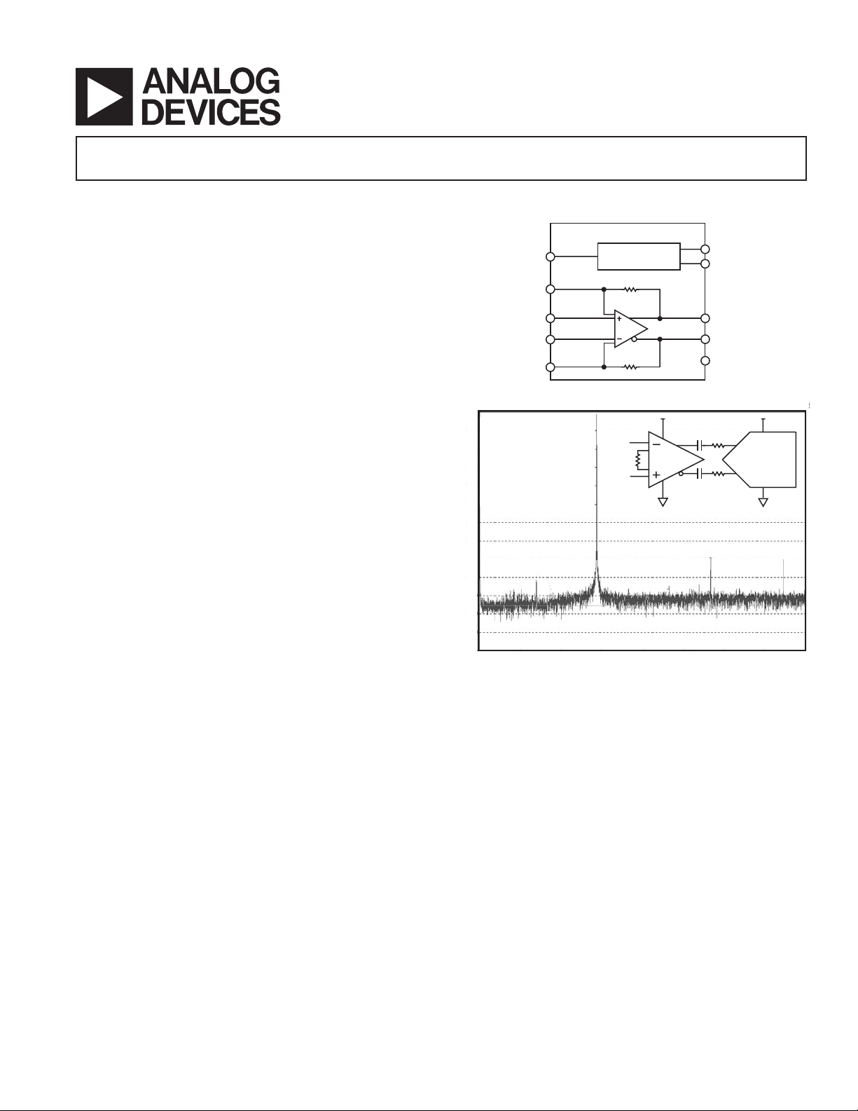
AD8351 WITH 10 dB OF
–10
GAIN DRIVING THE
AD6645 (RL = 1k⍀)
–20
ANALOG INPUT: 70MHz
ENCODE : 80MHz
–30
SNR : 69.1dB
FUND : –1.1dBFS
–40
HD2 : –78.5dBc
HD3 : –80.7dBc
–50
THD : –75.9dBc
SFDR : 78.2dBc
–60
–70
–80
–90
–100
–110
–120
–130
051015 20 25 30 35
+
BIAS CELL
INHI
RG
200⍀
INLO
AD8351
AD8351
100nF
100nF
VOCM
VPOS
OPHI
OPLO
COMM
25⍀
25⍀
2
AD6645
14-BIT ADC
3
GENERAL DESCRIPTION
The AD8351 is a low cost differential amplifier useful in RF and
IF applications up to 2.2 GHz. The voltage gain can be set from
unity to 26 dB using a single external gain resistor. The AD8351
provides a nominal 150 Ω differential output impedance. The
excellent distortion performance and low noise characteristics of
this device allow for a wide range of applications.
The AD8351 is designed to satisfy the demanding performance
requirements of communications transceiver applications. The
device can be used as a general-purpose gain block, an ADC driver,
REV. B
Information furnished by Analog Devices is believed to be accurate and
reliable. However, no responsibility is assumed by Analog Devices for its
use, nor for any infringements of patents or other rights of third parties that
may result from its use. No license is granted by implication or otherwise
under any patent or patent rights of Analog Devices. Trademarks and
registered trademarks are the property of their respective owners.
and a high speed data interface driver, among other functions. The
AD8351 can also be used as a single-ended-to-differential
amplifier with similar distortion products as in the differential
configuration. The exceptionally good distortion performance
makes the AD8351 an ideal solution for 12-bit and 14-bit IF
sampling receiver designs.
Fabricated in ADI’s high speed XFCB process, the AD8351
has high bandwidth that provides high frequency performance
and low distortion. The quiescent current of the AD8351 is 28 mA
typically. The AD8351 amplifier comes in a compact 10-lead
MSOP package and will operate over the temperature range
of –40°C to +85°C.
One Technology Way, P.O. Box 9106, Norwood, MA 02062-9106, U.S.A.
Tel: 781/329-4700 www.analog.com
Fax: 781/326-8703 © 2004 Analog Devices, Inc. All rights reserved.

(VS = 5 V, RL = 150 , RG = 110 (AV = 10 dB), f = 70 MHz, T = 25C, parameters
AD8351–SPECIFICATIONS
specified differentially, unless otherwise noted .)
Parameter Conditions Min Typ Max Unit
DYNAMIC PERFORMANCE
–3 dB Bandwidth GAIN = 6 dB, V
GAIN = 12 dB, V
GAIN = 18 dB, V
Bandwidth for 0.1 dB Flatness 0 dB ≤ GAIN ≤ 20 dB, V
Bandwidth for 0.2 dB Flatness 0 dB ≤ GAIN ≤ 20 dB, V
Gain Accuracy Using 1% Resistor for R
Gain Supply Sensitivity V
± 5% 0.08 dB/V
S
≤ 1.0 V p-p 3,000 MHz
OUT
≤ 1.0 V p-p 2,200 MHz
OUT
≤ 1.0 V p-p 600 MHz
OUT
≤ 1.0 V p-p 200 MHz
OUT
≤ 1.0 V p-p 400 MHz
OUT
, 0 dB ≤ AV ≤ 20 dB ± 1dB
G
Gain Temperature Sensitivity –40°C to +85°C 3.9 mdB/°C
Slew Rate R
= 1 kΩ, V
L
R
= 150 Ω, VS = 2 V Step 7,500 V/s
L
= 2 V Step 13,000 V/s
OUT
Settling Time 1 V Step to 1% <3 ns
Overdrive Recovery Time V
= 4 V to 0 V Step, V
IN
≤ ± 10 mV <2 ns
OUT
Reverse Isolation (S12) –67 dB
INPUT/OUTPUT CHARACTERISTICS
Input Common-Mode
Voltage Adjustment Range 1.2 to 3.8 V
Max Output Voltage Swing 1 dB Compressed 4.75 V p-p
Output Common-Mode Offset 40 mV
Output Common-Mode Drift –40°C to +85°C 0.24 mV/°C
Output Differential Offset Voltage
20 mV
Output Differential Offset Drift –40°C to +85°C 0.13 mV/°C
Input Bias Current ±15 A
Input Resistance
Input Capacitance
1
1
5kΩ
0.8 pF
CMRR 43 dB
Output Resistance
Output Capacitance
1
1
150 Ω
0.8 pF
POWER INTERFACE
Supply Voltage 3 5.5 V
PWUP Threshold 1.3 V
PWUP Input Bias Current PWUP at 5 V 100 A
PWUP at 0 V 25 A
Quiescent Current 28 32 mA
REV. B–2–

AD8351
Parameter Conditions Min Typ Max Unit
NOISE/DISTORTION
10 MHz
Second/Third Harmonic
Distortion
Third-Order IMD R
Output Third-Order Intercept f1 = 9.5 MHz, f2 = 10.5 MHz 33 dBm
Noise Spectral Density (RTI) 2.65 nV/√Hz
1 dB Compression Point 13.5 dBm
70 MHz
Second/Third Harmonic
Distortion
Third-Order IMD R
Output Third-Order Intercept f1 = 69.5 MHz, f2 = 70.5 MHz 31 dBm
Noise Spectral Density (RTI) 2.70 nV/√Hz
1 dB Compression Point 13.3 dBm
140 MHz
Second/Third Harmonic
Distortion
Third-Order IMD R
Output Third-Order Intercept f1 = 139.5 MHz, f2 = 140.5 MHz 29 dBm
Noise Spectral Density (RTI) 2.75 nV/√Hz
1 dB Compression Point 13 dBm
240 MHz
Second/Third Harmonic
Distortion
Third-Order IMD R
Output Third-Order Intercept f1 = 239.5 MHz, f2 = 240.5 MHz 27 dBm
Noise Spectral Density (RTI) 2.90 nV/√Hz
1 dB Compression Point 13 dBm
NOTES
1
Values are specified differentially.
2
See Applications section for single-ended-to-differential performance.
Specifications subject to change without notice.
2
2
2
2
RL = 1 kΩ, V
R
= 150 Ω, V
L
= 1 kΩ, f1 = 9.5 MHz, f2 = 10.5 MHz,
L
V
= 2 V p-p Composite –90 dBc
OUT
R
= 150 Ω, f1 = 9.5 MHz, f2 = 10.5 MHz,
L
V
= 2 V p-p Composite –70 dBc
OUT
RL = 1 kΩ, V
R
= 150 Ω, V
L
= 1 kΩ, f1 = 69.5 MHz, f2 = 70.5 MHz,
L
V
= 2 V p-p Composite –85 dBc
OUT
R
= 150 Ω, f1 = 69.5 MHz, f2 = 70.5 MHz,
L
V
= 2 V p-p Composite –69 dBc
OUT
RL = 1 kΩ, V
R
= 150 Ω, V
L
= 1 kΩ, f1 = 139.5 MHz, f2 = 140.5 MHz,
L
= 2 V p-p Composite –79 dBc
V
OUT
R
= 150 Ω, f1 = 139.5 MHz, f2 = 140.5 MHz,
L
= 2 V p-p Composite –67 dBc
V
OUT
RL = 1 kΩ, V
R
= 150 Ω, V
L
= 1 kΩ, f1 = 239.5 MHz, f2 = 240.5 MHz,
L
= 2 V p-p Composite –76 dBc
V
OUT
= 2 V p-p –95/–93 dBc
OUT
= 2 V p-p –86/–71 dBc
OUT
= 2 V p-p –79/–81 dBc
OUT
= 2 V p-p –65/–66 dBc
OUT
= 2 V p-p –69/–69 dBc
OUT
= 2 V p-p –54/–53 dBc
OUT
= 2 V p-p –60/–66 dBc
OUT
= 2 V p-p –46/–50 dBc
OUT
RL = 150 Ω, f1 = 239.5 MHz, f2 = 240.5 MHz,
V
= 2 V p-p Composite –62 dBc
OUT
REV. B
–3–

AD8351
ABSOLUTE MAXIMUM RATINGS*
PIN CONFIGURATION
Supply Voltage VPOS . . . . . . . . . . . . . . . . . . . . . . . . . . . . .6 V
PWUP Voltage . . . . . . . . . . . . . . . . . . . . . . . . . . . . . . . VPOS
Internal Power Dissipation . . . . . . . . . . . . . . . . . . . . . 320 mW
. . . . . . . . . . . . . . . . . . . . . . . . . . . . . . . . . . . . . . . 125°C/W
JA
Maximum Junction Temperature . . . . . . . . . . . . . . . . . 125°C
Operating Temperature Range . . . . . . . . . . . . –40°C to +85°C
Storage Temperature Range . . . . . . . . . . . . . –65°C to +150°C
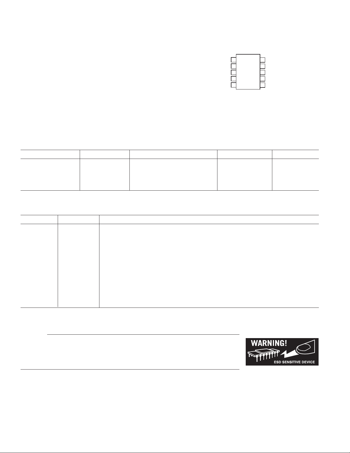
PWUP
RGP1
INHI
INLO
RGP2
1
2
AD8351
3
TOP VIEW
(Not to Scale)
4
5
10
9
8
7
6
VOCM
VPOS
OPHI
OPLO
COMM
Lead Temperature Range (Soldering 60 sec) . . . . . . . . . 300°C
*Stresses above those listed under Absolute Maximum Ratings may cause perma-
nent damage to the device. This is a stress rating only; functional operation of the
device at these or any other conditions above those indicated in the operational
section of this specification is not implied. Exposure to absolute maximum rating
conditions for extended periods may affect device reliability.
ORDERING GUIDE
Model Temp. Range Package Description Package Option Branding
AD8351ARM –40°C to +85°C 10-Lead MSOP, 7" Tape and Reel RM-10 JDA
AD8351ARM-R2 –40°C to +85°C 10-Lead MSOP, 7" Tape and Reel RM-10 JDA
AD8351ARM-REEL7 –40°C to +85°C 10-Lead MSOP, 7" Tape and Reel RM-10 JDA
AD8351-EVAL Evaluation Board
PIN FUNCTION DESCRIPTIONS
Pin No. Name Function
1PWUP Apply a positive voltage (1.3 V ≤ V
≤ VPOS ) to activate device.
PWUP
2 RGP1 Gain Resistor Input 1.
3 INHI Balanced Differential Input. Biased to midsupply, typically ac-coupled
4 INLO Balanced Differential Input. Biased to midsupply, typically ac-coupled.
5 RGP2 Gain Resistor Input 2.
6 COMM Device Common. Connect to low impedance ground.
7 OPLO Balanced Differential Output. Biased to VOCM, typically ac-coupled.
8 OPHI Balanced Differential Output. Biased to VOCM, typically ac-coupled.
9 VPOS Positive Supply Voltage. 3 V to 5.5 V.
10 VOCM Voltage applied to this pin sets the common-mode voltage at both the input and output.
Typically decoupled to ground with a 0.1 µF capacitor.
CAUTION
ESD (electrostatic discharge) sensitive device. Electrostatic charges as high as 4000 V readily
accumulate on the human body and test equipment and can discharge without detection. Although the
AD8351 features proprietary ESD protection circuitry, permanent damage may occur on devices
subjected to high energy electrostatic discharges. Therefore, proper ESD precautions are recommended
to avoid performance degradation or loss of functionality.
–4–
REV. B

(VS = 5 V, T = 25ⴗC, unless otherwise noted.)
FREQUENCY (MHz)
30
1 10000
GAIN (dB)
5
10 100 1000
25
20
15
10
0
RG = 10⍀
RG = 50⍀
RG = 200⍀
20
15
10
RG = 20⍀
RG = 80⍀
Typical Performance Characteristics–
AD8351
GAIN (dB)
5
0
–5
1 10000
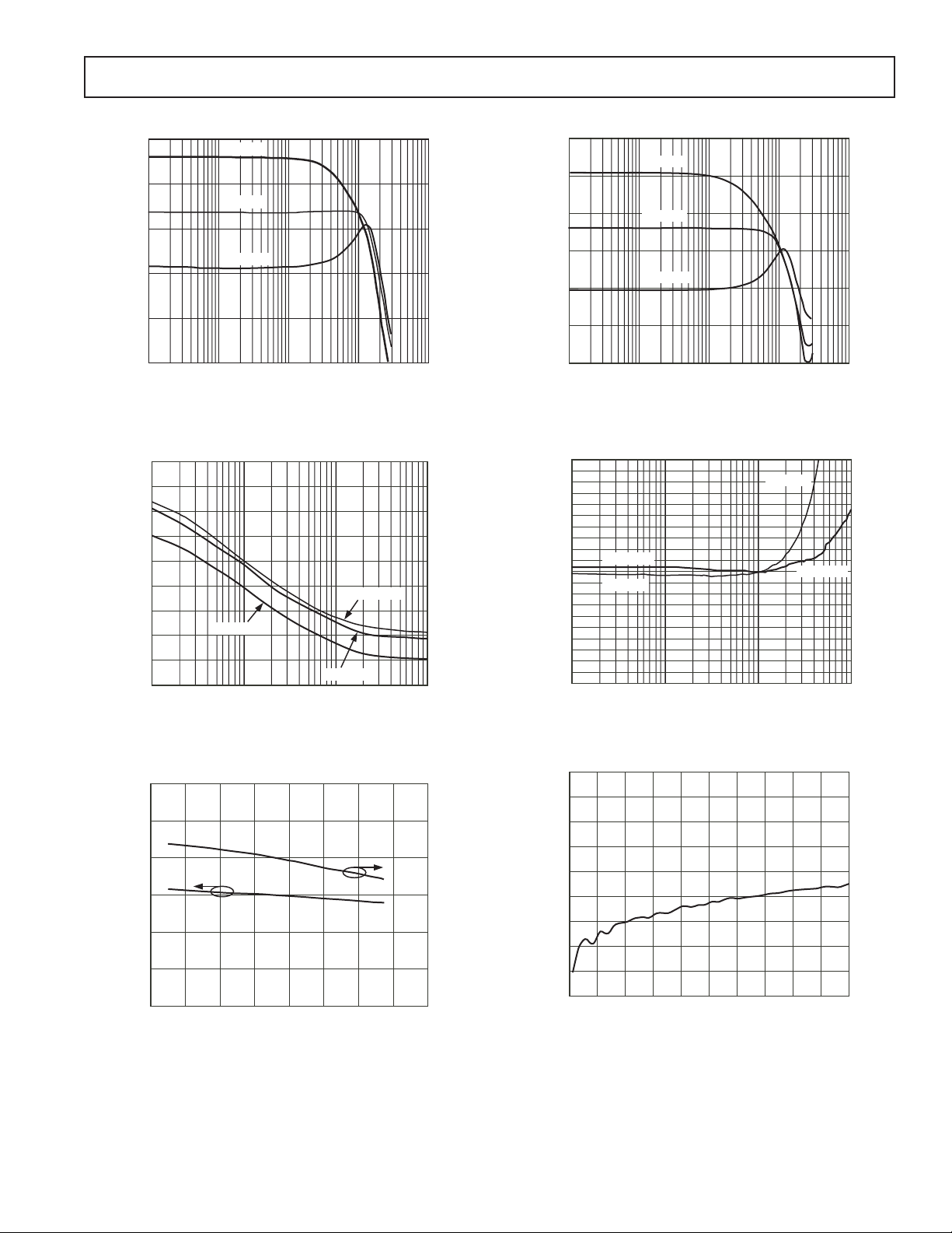
TPC 1. Gain vs. Frequency for a 150 Ω Differential Load
= 6 dB, 12 dB, and 18 dB)
(A
V
35
30
25
20
15
10
GAIN (dB)
5
0
–5
–10
10 10k
TPC 2. Gain vs. Gain Resistor, RG (f = 100 MHz,
= 150 Ω, 1 kΩ, and Open)
R
L
10.75
10.50
10.25
10.00
= 1k⍀) (dB)
L
9.75
GAIN (R
9.50
9.25
TPC 3. Gain vs. Temperature at 100 MHz (AV = 10 dB)
–30 50
–50 110
RG = 200⍀
10 100 1000
FREQUENCY (MHz)
RL = OPEN
R
= 150⍀
L
= 1k⍀
R
L
100 1k
RG (⍀)
–10 10 30 70 90
TEMPERATURE (ⴗC)
10.50
10.25
10.00
9.75
9.50
9.25
9.00
GAIN (RL = 150⍀) (dB)
TPC 4. Gain vs. Frequency for a 1 kΩ Differential Load
= 10 dB, 18 dB, and 26 dB)
(A
V
1.0
0.9
0.8
0.7
0.6
0.5
0.4
0.3
0.2
0.1
–0.1
–0.2
–0.3
GAIN FLATNESS (dB)
–0.4
–0.5
–0.6
–0.7
–0.8
–0.9
–1.0
RL = 150⍀
0
RL = 1k⍀
1 1000
10 100
FREQUENCY (MHz)
RL = 1k⍀
RL = 150⍀
TPC 5. Gain Flatness vs. Frequency
(R
= 150 Ω and 1 kΩ, AV =10 dB)
L
0
–10
–20
–30
–40
–50
ISOLATION (dB)
–60
–70
–80
–90
0 1000
100 200 300 400 500 600 700 800 900
FREQUENCY (MHz)
TPC 6. Isolation vs. Frequency (AV = 10 dB)
REV. B
–5–
 Loading...