700 MHz to 2700 MHz
C
C
FEATURES
Output frequency range: 700 MHz to 2700 MHz
Modulation bandwidth: dc to 160 MHz (large signal BW)
1 dB output compression: 5.6 dBm @ 2140 MHz
Output disable function: output below –50 dBm in < 50 ns
Noise floor: –156 dBm/Hz
Phase quadrature error: 0.3 degrees @ 2140 MHz
Amplitude balance: 0.1 dB
Single supply: 4.75 V to 5.5 V
Pin compatible with AD8345/AD8346s
16-lead, exposed-paddle TSSOP package
APPLICATIONS
Cellular/PCS communication systems infrastructure
WCDMA/CDMA2000/PCS/GSM/EDGE
Wireless LAN/wireless local loop
LMDS/broadband wireless access systems
Quadrature Modulator
AD8349
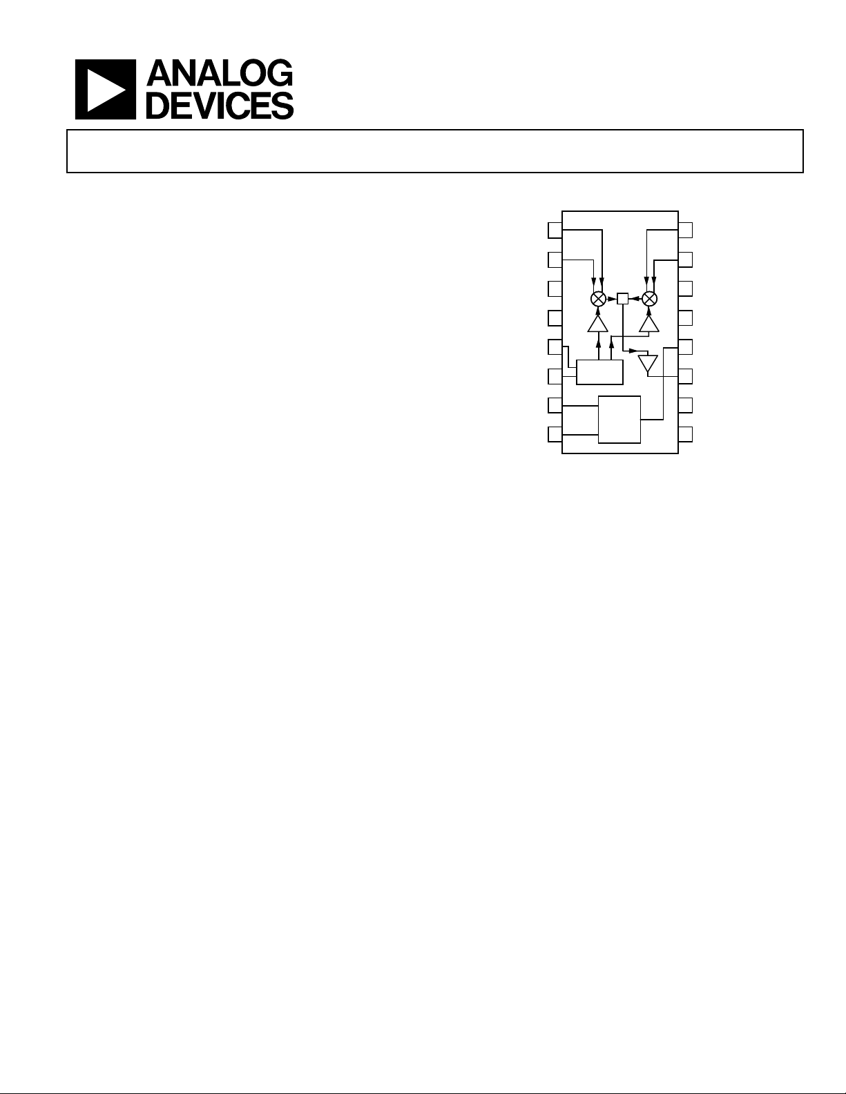
FUNCTIONAL BLOCK DIAGRAM
IBBP
IBBN
OM1
OM1
LOIN
LOIP
VPS1
ENOP
1
2
3
4
5
6
7
8
AD8349
PHASE
SPLITTER
Σ
BIAS
Figure 1.
16
QBBP
15
QBBN
14
COM3
13
COM3
12
VPS2
11
VOUT
10
COM3
9
COM2
03570-0-001
PRODUCT DESCRIPTION
The AD8349 is a silicon, monolithic, RF quadrature modulator
that is designed for use from 700 MHz to 2700 MHz. Its
excellent phase accuracy and amplitude balance enable high
performance direct RF modulation for communication systems.
The differential LO input signal is buffered, and then split into
an in-phase (I) signal and a quadrature-phase (Q) signal using a
polyphase phase splitter. These two LO signals are further
buffered and then mixed with the corresponding I channel and
Q channel baseband signals in two Gilbert cell mixers. The
mixers’ outputs are then summed together in the output
amplifier. The output amplifier is designed to drive 50 Ω loads.
The RF output can be switched on and off within 50 ns by
applying a control pulse to the ENOP pin.
The AD8349 can be used as a direct-to-RF modulator in digital
communication systems such as GSM, CDMA, and WCDMA
base stations, and QPSK or QAM broadband wireless access
transmitters. Its high dynamic range and high modulation
accuracy also make it a perfect IF modulator in local multipoint
distribution systems (LMDS) using complex modulation
formats.
The AD8349 is fabricated using Analog Devices’ advanced
complementary silicon bipolar process, and is available in a 16lead, exposed-paddle TSSOP package. Its performance is
specified over a –40°C to +85°C temperature range.
Rev. A
Information furnished by Analog Devices is believed to be accurate and reliable.
However, no responsibility is assumed by Analog Devices for its use, nor for any
infringements of patents or other rights of third parties that may result from its use.
Specifications subject to change without notice. No license is granted by implication
or otherwise under any patent or patent rights of Analog Devices. Trademarks and
registered trademarks are the property of their respective owners.
One Technology Way, P.O. Box 9106, Norwood, MA 02062-9106, U.S.A.
Tel: 781.329.4700
Fax: 781.326.8703 © 2004 Analog Devices, Inc. All rights reserved.
www.analog.com

AD8349
TABLE OF CONTENTS
Specifications..................................................................................... 3
Absolute Maximum Ratings............................................................ 5
ESD Caution.................................................................................. 5
Pin Configuration and Functional Descriptions.......................... 6
Equivalent Circuits........................................................................... 7
Typical Performance Characteristics............................................. 8
Circuit Description......................................................................... 14
Overview...................................................................................... 14
LO Interface................................................................................. 14
V-to-I Converter......................................................................... 14
Mixers .......................................................................................... 14
D-to-S Amplifier......................................................................... 14
Bias Circuit ..................................................................................14
Output Enable............................................................................. 14
Basic Connections .......................................................................... 15
Baseband I and Q Inputs........................................................... 15
Single-Ended Baseband Drive .................................................. 15
LO Input Drive Level ................................................................. 16
Frequency Range ........................................................................ 16
LO Input Impedance Matching ................................................16
Single-Ended LO Drive.............................................................. 17
RF Output.................................................................................... 17
Output Enable............................................................................. 17
Baseband DAC Interface........................................................... 18
AD9777 Interface ....................................................................... 18
Biasing and Filtering.................................................................. 18
Reducing Undesired Sideband Leakage .................................. 19
Reduction of LO Feedthrough ................................................. 19
Sideband Suppression and LO Feedthrough vs. Temperature
....................................................................................................... 20
Applications..................................................................................... 21
3GPP WCDMA Single-Carrier Application........................... 21
WCDMA MultiCarrier Application ........................................ 21
GSM/EDGE Application........................................................... 22
Soldering Information ............................................................... 23
LO Generation Using PLLs....................................................... 23
Transm i t DAC O p tions ............................................................. 23
Evaluation Board ............................................................................ 24
Characterization Setups................................................................. 26
SSB Setup..................................................................................... 26
Outline Dimensions....................................................................... 27
Ordering Guide .......................................................................... 27
REVISION HISTORY
11/04—Data Sheet Changed from Rev. 0 to Rev. A
Changes to Figure 25 through Figure 30 ................................11
Changes to Figure 37 through Figure 39 ................................13
Change to WCDMA MultiCarrier Application section .......21
Change to Figure 60 and Figure 61 .........................................21
11/03—Revision 0: Initial Version
Rev. A | Page 2 of 28

AD8349
SPECIFICATIONS
VS = 5 V; ambient temperature (TA) = 25°C; LO = –6 dBm; I/Q inputs = 1.2 V p-p differential sine waves in quadrature on a 400 mV dc
bias; baseband frequency = 1 MHz; LO source and RF output load impedances are 50 Ω, unless otherwise noted.
Table 1.
Parameter Conditions Min Typ Max Unit
Operating Frequency 700 2700 MHz
LO = 900 MHz
Output Power 1.5 4 6 dBm
Output P1 dB 7.6 dBm
Carrier Feedthrough –45 –30 dBm
Sideband Suppression –35 –31 dBc
Third Harmonic
Output IP3 F1BB = 3 MHz, F2BB = 4 MHz, P
Quadrature Error 1.9 degree
I/Q Amplitude Balance 0.1 dB
Noise Floor 20 MHz offset from LO, all BB inputs 400 mV dc bias only –155 dBm/Hz
20 MHz offset from LO, BB inputs = 1.2 V p-p differential on 400 mV dc –150 dBm/Hz
GSM Sideband Noise LO = 884.8 MHz, 6 MHz offset from LO, P
LO = 1900 MHz
Output Power 0 3.8 6 dBm
Output P1dB 6.8 dBm
Carrier Feedthrough –38 dBm
Sideband Suppression –40 –36 dBc
Third Harmonic
Output IP3 F1BB = 3 MHz, F2BB = 4 MHz, P
Quadrature Error 0.7 degree
I/Q Amplitude Balance 0.1 dB
Noise Floor 20 MHz offset from LO, all BB inputs 400 mV dc bias only –156 dBm/Hz
20 MHz offset from LO, BB inputs = 1.2 V p-p differential on 400 mV dc –150 dBm/Hz
GSM Sideband Noise LO = 1960 MHz, 6 MHz offset from LO, P
LO = 2140 MHz
Output Power –2 2.4 5.1 dBm
Output P1dB 5.6 dBm
Carrier Feedthrough –42 –30 dBm
Sideband Suppression –43 –36 dBc
Third Harmonic
Output IP3 F1BB = 3 MHz, F2BB = 4 MHz, P
Quadrature Error 0.3 degree
I/Q Amplitude Balance 0.1 dB
Noise Floor 20 MHz offset from LO, all BB inputs 400 mV dc bias only –156 dBm/Hz
20 MHz offset from LO, BB inputs = 1.2 V p-p differential on 400 mV dc –151 dBm/Hz
WCDMA Noise Floor LO = 2140 MHz. 30 MHz offset from LO, P
LO INPUTS Pins LOIP and LOIN
LO Drive Level Characterization performed at typical level –10 –6 0 dBm
Nominal Impedance 50 Ω
Input Return Loss Drive via 1:1 balun, LO = 2140 MHz –8.6 dB
BASEBAND INPUTS Pins IBBP, IBBN, QBBP, QBBN
I and Q Input Bias Level 400 mV
Input Bias Current 11 µA
Input Offset Current 1.8 µA
Bandwidth (0.1 dB) LO = 1500 MHz, baseband input = 600 mV p-p sine wave on 400 mV dc 10 MHz
LO = 1500 MHz, baseband input = 60 mV p-p sine wave on 400 mV dc 24 MHz
1
1
1
P
– (FLO + (3 × FBB)), P
OUT
P
– (FLO + (3 × FBB)), P
OUT
P
– (FLO + (3 × FBB)), P
OUT
= 4 dBm –39 –36 dBc
OUT
= -4.2 dBm 21 dBm
OUT
= 2 dBm –152 dBc/Hz
OUT
= 3.8 dBm –37 –36 dBc
OUT
= –4.5 dBm 22 dBm
OUT
= 2 dBm –151 dBc/Hz
OUT
= 2.4 dBm –37 –36 dBc
OUT
= –6.5 dBm 19 dBm
OUT
= –17.3 dBm –156 dBm/Hz
CHAN
Rev. A | Page 3 of 28

AD8349
Parameter Conditions Min Typ Max Unit
Bandwidth (3 dB) LO = 1500 MHz, baseband input = 600 mV p-p sine wave on 400 mV dc 160 MHz
LO = 1500 MHz, baseband input = 60 mV p-p sine wave on 400 mV dc 340 MHz
OUTPUT ENABLE Pin ENOP
Off Isolation ENOP Low –78 –50 dBm
Turn-On Settling Time ENOP Low to High (90% of envelope) 20 ns
Turn-Off Settling Time ENOP High to Low (10% of envelope) 50 ns
ENOP High Level (Logic 1) 2.0 V
ENOP Low Level (Logic 0) 0.8 V
POWER SUPPLIES Pins VPS1 and VPS2
Voltage 4.75 5.5 V
Supply Current ENOP = High 135 150 mA
ENOP = Low 130 145 mA
1
The amplitude of the third harmonic relative to the single sideband power decreases with decreasing baseband drive level (see Figure 19, Figure 20, and Figure 21).
Rev. A | Page 4 of 28

AD8349
ABSOLUTE MAXIMUM RATINGS
Table 2.
Parameter Rating
Supply Voltage VPOS 5.5 V
IBBP, IBBN, QBBP, QBBN 0 V, 2.5 V
LOIP and LOIN 10 dBm
Internal Power Dissipation 800 mW
θJA (Exposed Paddle Soldered Down) 30°C/W
Maximum Junction Temperature 125°C
Operating Temperature Range −40°C to +85°C
Storage Temperature Range −65°C to +150°C
ESD CAUTION
ESD (electrostatic discharge) sensitive device. Electrostatic charges as high as 4000 V readily accumulate on
the human body and test equipment and can discharge without detection. Although this product features
proprietary ESD protection circuitry, permanent damage may occur on devices subjected to high energy
electrostatic discharges. Therefore, proper ESD precautions are recommended to avoid performance
degradation or loss of functionality.
Stresses above those listed under Absolute Maximum Ratings
may cause permanent damage to the device. This is a stress
rating only; functional operation of the device at these or any
other conditions above those indicated in the operational
section of this specification is not implied. Exposure to absolute
maximum rating conditions for extended periods may affect
device reliability.
Rev. A | Page 5 of 28
AD8349
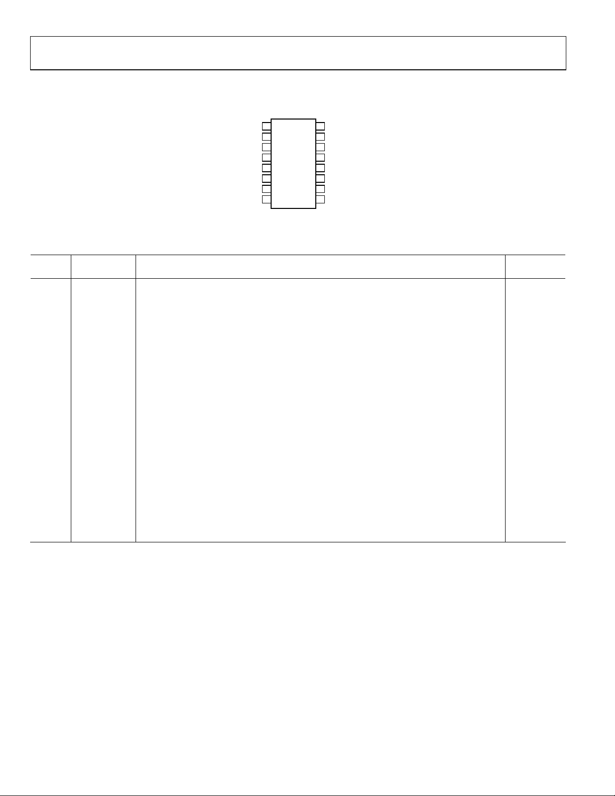
PIN CONFIGURATION AND FUNCTIONAL DESCRIPTIONS
Table 3. Pin Function Descriptions
Pin No. Mnemonic Description
1, 2,
15, 16
IBBP, IBBN,
QBBN, QBBP
Differential In-Phase and Quadrature Baseband Inputs. These high impedance inputs must be
dc-biased to approximately 400 mV dc, and must be driven from a low impedance source.
Nominal characterized ac signal swing is 600 mV p-p on each pin (100 mV to 700 mV). This
results in a differential drive of 1.2 V p-p with a 400 mV dc bias. These inputs are not self-biased
and must be externally biased.
3, 4 COM1
Common Pin for LO Phase Splitter and LO Buffers. COM1, COM2, and COM3 should all be
connected to a ground plane via a low impedance path.
5, 6 LOIN, LOIP
Differential Local Oscillator Inputs. Internally dc-biased to approximately 1.8 V when V
Pins must be ac-coupled. Single-ended drive is possible with degradation in performance.
7 VPS1
Positive Supply Voltage (4.75 V to 5.5 V) for the LO Bias-Cell and Buffer. VPS1 and VPS2 should
be connected to the same supply. To ensure adequate external bypassing, connect 0.1 µF and
100 pF capacitors between VPS1 and ground.
8 ENOP
Output Enable. This pin can be used to enable or disable the RF output. Connect to high logic
level for normal operation. Connect to low logic level to disable output.
9 COM2
Common Pin for the Output Amplifier. COM1, COM2, and COM3 should all be connected to a
ground plane via a low impedance path.
10, 13,
14
11 VOUT
COM3
Common Pin for Input V-to-I Converters and Mixer Cores. COM1, COM2, and COM3 should all
be connected to a ground plane via a low impedance path.
Device Output. Single-ended, 50 Ω internally biased RF output. Pin must be ac-coupled to the
load.
12 VPS2
Positive Supply Voltage (4.75 V to 5.5 V) for the Baseband Input V-to-I Converters, Mixer Core,
Band Gap Reference, and Output Amplifer. VPS1 and VPS2 should be connected to the same
supply. To ensure adequate external bypassing, connect 0.1 µF and 100 pF capacitors between
VPS2 and ground.
IBBP
IBBN
COM1
COM1
LOIN
LOIP
VPS1
ENOP
1
AD8349
2
3
TOP VIEW
(Not to Scale)
4
5
6
7
8
Figure 2.
16
QBBP
15
QBBN
14
COM3
COM3
13
12
VPS2
VOUT
11
COM3
10
COM2
9
03570-0-002
Equivalent
Circuit
Circuit A
= 5.0 V.
S
Circuit B
Circuit C
Circuit D
Rev. A | Page 6 of 28
AD8349
C
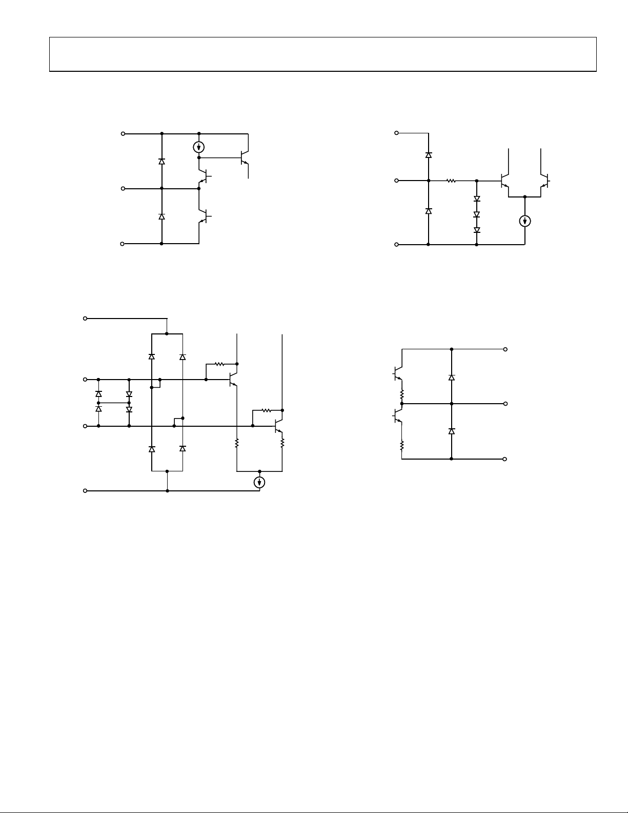
EQUIVALENT CIRCUITS
VPS2
VPS2
VPS1
LOIN
LOIP
OM1
IBBP
COM3
Figure 3. Circuit A
03570-0-003
03570-0-004
ENOP
COM3
40Ω
40Ω
Figure 5. Circuit C
VPS2
VOUT
COM2
03570-0-006
04500-0-005
Figure 4. Circuit B
Figure 6. Circuit D
Rev. A | Page 7 of 28
AD8349
TYPICAL PERFORMANCE CHARACTERISTICS
8
7
6
5
4
3
2
1
0
–1
SSB OUTPUT POWER (dBm)
–2
–3
–4
700 900 1100 1300 1500 1700 1900 2100 2300 2500 2700
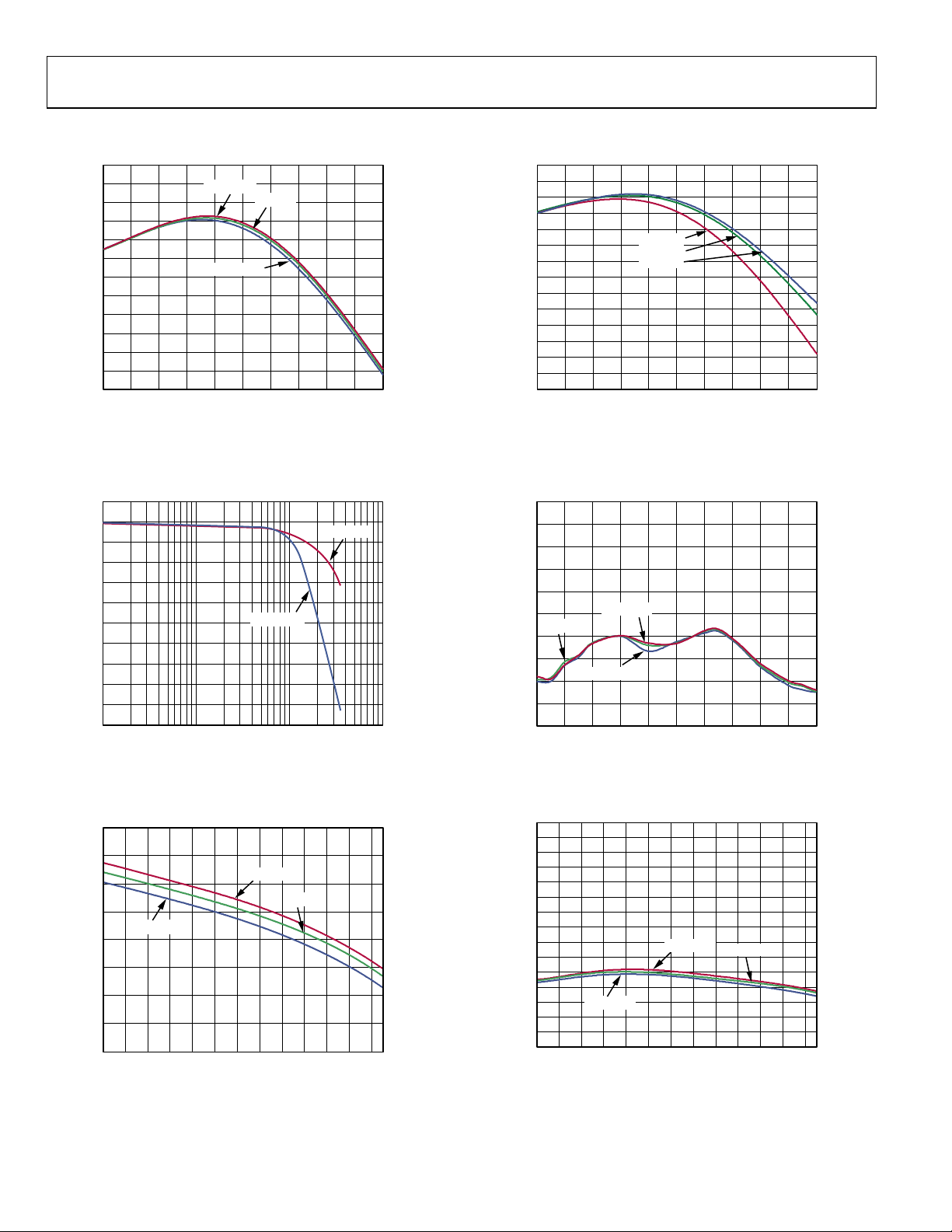
Figure 7. Single Sideband (SSB) Output Power (P
(I and Q Inputs Driven in Quadrature at Baseband Frequency (F
I and Q Inputs at 1.2 V p-p Differential, T
VS = 5.25V
VS = 5V
VS = 4.75V
LO FREQUENCY (MHz)
) vs. LO Frequency (FLO)
OUT
= 25°C)
A
) = 1 MHz,
BB
03570-0-007
10
9
8
7
6
5
4
3
2
1
0
–1
1dB OUTPUT COMPRESSION (dBm)
–2
–3
–4
700 900 1100 1300 1500 1700 1900 2100 2300 2500 2700
T = +85°C
°
C
T = +25
°
C
T = –40
LO FREQUENCY (MHz)
Figure 10. SSB Output 1 dB Compression Point (OP1dB) vs. F
I and Q Inputs Driven in Quadrature , T
= 25°C)
A
(FBB = 1 MHz,
LO
03570-0-010
1
0
–1
–2
–3
–4
–5
–6
–7
–8
OUTPUT POWER VARIATION (dB)
–9
–10
1 10 1000100
BASEBAND FREQUENCY (MHz)
600mV p-p
Figure 8. I and Q Input Bandwidth Normalized to Gain @ 1 MHz
= 1500 MHz, TA = 25°C)
(F
LO
4.0
3.5
3.0
2.5
2.0
1.5
1.0
SSB OUTPUT POWER (dBm)
0.5
Figure 9. SSB P
VS = 4.75V
0
–40–30–20–100 10203040
TEMPERATURE (°C)
vs. Temperature (FLO = 2140 MHz, FBB = 1 MHz, I and Q
OUT
VS = 5.25V
VS = 5V
Inputs Driven in Quadrature at 1.2 V p-p Differential)
60mV p-p
6050 70 80
03570-0-008
03570-0-009
–10
–15
–20
–25
–30
–35
VS = 5V
–40
–45
–50
CARRIER FEEDTHROUGH (dBm)
–55
–60
700 900 1100 1300 1500 1700 1900 2100 2300 2500 2700
Figure 11. Carrier Feedthrough vs. F
VS = 5.25V
VS = 4.75V
LO FREQUENCY (MHz)
(FBB = 1 MHz, I and Q Inputs Driven in
LO
Quadrature at 1.2 V p-p Differential, TA = 25°C)
–20
–22
–24
–26
–28
–30
–32
–34
–36
–38
–40
–42
–44
CARRIER FEEDTHROUGH (dBm)
–46
–48
–50
–40–30–20–100 10203040
VS = 4.75V
Figure 12. Carrier Feedthrough vs. Temperature (F
VS = 5.25V
TEMPERATURE (
VS = 5V
6050 70 80
°
C)
= 2140 MHz, FBB = 1 MHz,
LO
I and Q Inputs Driven in Quadrature at 1.2 V p-p Differential, T
= 25°C)
A
03570-0-011
03570-0-012
Rev. A | Page 8 of 28
AD8349
–10
–15
–20
–25
–30
–35
–40
–45
–50
SIDEBAND SUPPRESSION (dBc)
–55
–60
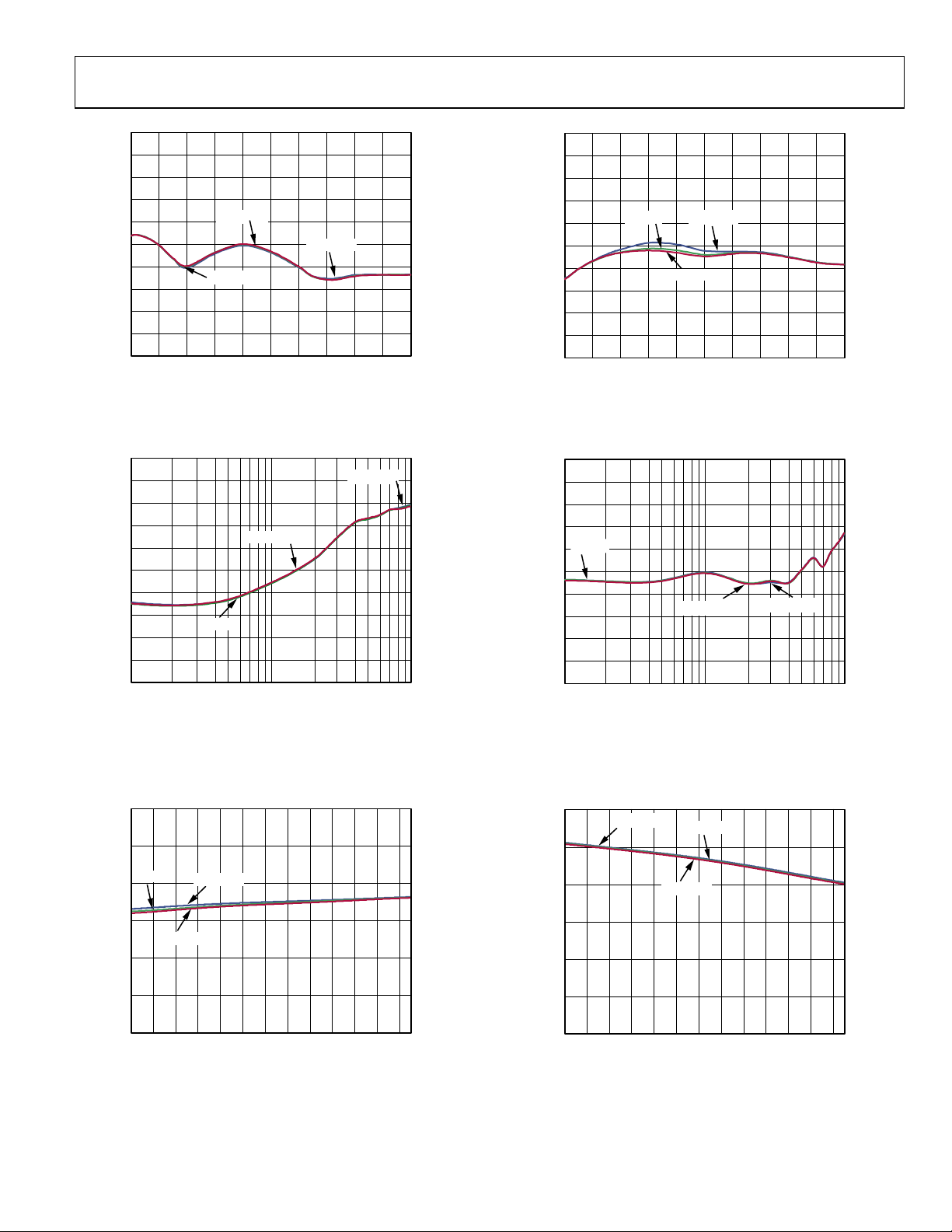
700 900 1100 1300 1500 1700 1900 2100 2300 2500 2700
Figure 13. Sideband Suppression vs. F
VS = 5.25V
VS = 5V
LO FREQUENCY (MHz)
LO
VS = 4.75V
(FBB = 1 MHz, I and Q Inputs
Driven in Quadrature at 1.2 V p-p Differential, T
= 25°C)
A
03570-0013
–10
–15
–20
–25
–30
–35
–40
–45
–50
THIRD ORDER DISTORTION (dBc)
–55
–60
700 900 1100 1300 1500 1700 1900 2100 2300 2500 2700
VS = 5V
Figure 16. Third Order Distortion vs. F
VS = 4.75V
VS = 5.25V
LO FREQUENCY (MHz)
(FBB = 1 MHz, I and Q Inputs
LO
Driven in Quadrature at 1.2 V p-p Differential, TA = 25°C)
03570-0016
–10
–15
–20
–25
–30
–35
–40
–45
–50
SIDEBAND SUPPRESSION (dBc)
–55
–60
1 10 100
VS = 5V
BASEBAND FREQUENCY (MHz)
Figure 14. Sideband Suppression vs. F
VS = 5.25V
(FLO = 2140 MHz, I and Q Inputs
BB
Driven in Quadrature at 1.2 V p-p Differential, T
–30
–35
–40
VS = 5V
VS = 4.75V
VS = 4.75V
= 25°C)
A
03570-0-014
–10
–15
–20
–25
VS = 5V
–30
–35
–40
–45
–50
THIRD ORDER DISTORTION (dBc)
–55
–60
1 10 100
BASEBAND FREQUENCY (MHz)
Figure 17. Third Order Distortion vs. F
VS = 5.25V
(FLO = 2140 MHz, I and Q Inputs
BB
VS = 4.75V
Driven in Quadrature at 1.2 V p-p Differential, T
–30
–35
–40
VS = 4.75V
VS = 5V
VS = 5.25V
= 25°C)
A
03570-0-017
–45
VS = 5.25V
–50
SIDEBAND SUPPRESSION (dBc)
–55
–60
–40–30–20–100 10203040
TEMPERATURE (
°
Figure 15. Sideband Suppression vs. Temperature (F
F
= 1 MHz, I and Q Inputs Driven in Quadrature at 1.2 V p-p Differential)
BB
6050 70 80
C)
= 2140 MHz,
LO
03570-0-015
F
Rev. A | Page 9 of 28
–45
–50
THIRD ORDER DISTORTION (dBc)
–55
–60
–40–30–20–100 10203040
TEMPERATURE (
°
Figure 18. Third Order Distortion vs. Temperature (F
= 1 MHz, I and Q Inputs Driven in Quadrature at 1.2 V p -p Differential)
BB
6050 70 80
C)
= 2140 MHz,
LO
03570-0-018
 Loading...