

Page 1
O
S
V
50 MHz to 1000 MHz
FEATURES
Integrated I/Q demodulator with IF VGA amplifier
Operating IF frequency 50 MHz to 1000 MHz
(3 dB IF BW of 500 MHz driven from R
Demodulation bandwidth 75 MHz
Linear-in-decibel AGC range 44 dB
Third-order intercept
IIP3 +28 dBm @ minimum gain (FIF = 380 MHz)
IIP3 −8 dBm @ maximum gain (F
Quadrature demodulation accuracy
Phase accuracy 0.5°
Amplitude balance 0.25 dB
Noise figure 11 dB @ maximum gain (FIF = 380 MHz)
LO input −10 dBm
Single supply 2.7 V to 5.5 V
Power-down mode
Compact, 28-lead TSSOP package
APPLICATIONS
QAM/QPSK demodulator
W-CDMA/CDMA/GSM/NADC
Wireless local loop
LMDS
GENERAL DESCRIPTION
= 200 Ω)
S
= 380 MHz)
IF
ENBL
VGIN
IFIP
IFIN
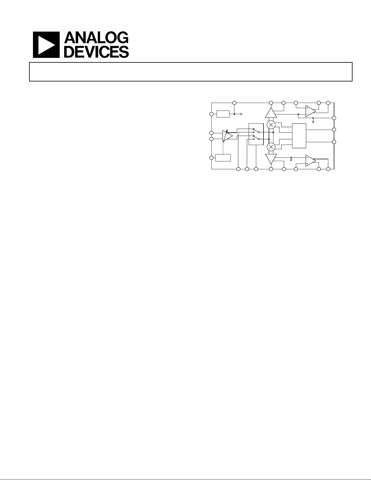
Quadrature Demodulator
AD8348
FUNCTIONAL BLOCK DIAGRAM
IMX
IOF
13
16
QOFS
VCMO
IAIN
6
DIVIDE
BY 2
PHASE
SPLITTER
23
QAIN
VCMO
15
11
10
17
BIAS
CELL
GAIN
CONTROL
REF
24
ENVG21QXMO
8
14
VREF
18
19
MXIN
MXIP
Figure 1.
IOPP3IOPN
4
AD8348
25
QOPP26QOPN
VCMO
5
LOIP
1
28
LOIN
03678-001
The AD8348 is a broadband quadrature demodulator with an
integrated intermediate frequency (IF), variable gain amplifier
(VGA), and integrated baseband amplifiers. It is suitable for use in
communications receivers, performing quadrature demodulation
from IF directly to baseband frequencies. The baseband amplifiers
are designed to interface directly with dual-channel ADCs, such
as the
AD9201, AD9283, and AD9218, for digitizing and post-
processing.
The IF input signal is fed into two Gilbert cell mixers through
an X-AMP® VGA. The IF VGA provides 44 dB of gain control.
A precision gain control circuit sets a linear-in-decibel gain characteristic for the VGA and provides temperature compensation.
The LO quadrature phase splitter employs a divide-by-2 frequency
divider to achieve high quadrature accuracy and amplitude balance
over the entire operating frequency range.
Optionally, the IF VGA can be disabled and bypassed. In this
mode, the IF signal is applied directly to the quadrature mixer
inputs via the MXIP and MXIN pins.
Rev. A
Information furnished by Analog Devices is believed to be accurate and reliable. However, no
responsibility is assumed by Anal og Devices for its use, nor for any infringements of patents or ot her
rights of third parties that may result from its use. Specifications subject to change without notice. No
license is granted by implication or otherwise under any patent or patent rights of Analog Devices.
Trademarks and registered trademarks are the property of their respective owners.
Separate I- and Q-channel baseband amplifiers follow the baseband
outputs of the mixers. The voltage applied to the VCMO pin sets
the dc common-mode voltage level at the baseband outputs.
Typically, VCMO is connected to the internal VREF voltage, but
it can also be connected to an external voltage. This flexibility
allows the user to maximize the input dynamic range to the ADC.
Connecting a bypass capacitor at each offset compensation input
(IOFS and QOFS) nulls dc offsets produced in the mixer. Offset
compensation can be overridden by applying an external voltage
at the offset compensation inputs.
The mixers’ outputs are brought off-chip for optional filtering
before final amplification. Inserting a channel selection filter
before each baseband amplifier increases the baseband amplifiers’
signal handling range by reducing the amplitude of high level,
out-of-channel interferers before the baseband signal is fed into
the I/Q baseband amplifiers. The single-ended mixer output is
amplified and converted to a differential signal for driving ADCs.
One Technology Way, P.O. Box 9106, Norwood, MA 02062-9106, U.S.A.
Tel: 781.329.4700 www.analog.com
Fax: 781.461.3113 ©2006 Analog Devices, Inc. All rights reserved.
Page 2

AD8348
TABLE OF CONTENTS
Features .............................................................................................. 1
Enable........................................................................................... 18
Applications....................................................................................... 1
Functional Block Diagram .............................................................. 1
General Description......................................................................... 1
Revision History ............................................................................... 2
Specifications..................................................................................... 3
Absolute Maximum Ratings............................................................ 6
ESD Caution.................................................................................. 6
Pin Configuration and Function Descriptions............................. 7
Equivalent Circuits........................................................................... 9
Typical Performance Characteristics ........................................... 11
VGA and Demodulator .............................................................11
Demodulator Using MXIP and MXIN.................................... 14
Final Baseband Amplifiers ........................................................15
VGA/Demodulator and Baseband Amplifier......................... 16
Theory of Operation ...................................................................... 18
Baseband Offset Cancellation................................................... 18
Applications..................................................................................... 20
Basic Connections...................................................................... 20
Power Supply............................................................................... 20
Device Enable ............................................................................. 20
VGA Enable ................................................................................ 20
Gain Control............................................................................... 20
LO Inputs..................................................................................... 20
IF Inputs ...................................................................................... 20
MX Inputs ................................................................................... 20
Baseband Outputs ...................................................................... 21
Output DC Bias Level................................................................ 21
Interfacing to Detector for AGC Operation............................... 21
Baseband Filters.......................................................................... 22
LO Generation ............................................................................ 23
VGA.............................................................................................. 18
Downconversion Mixers ........................................................... 18
Phase Splitter............................................................................... 18
I/Q Baseband Amplifiers........................................................... 18
REVISION HISTORY
4/06—Rev. 0 to Rev. A
Updated Format..................................................................Universal
Changes to Specifications................................................................ 3
Changes to IF Inputs Section ........................................................20
Changes to Evaluation Board Section.......................................... 23
Changes to Table 6.......................................................................... 27
Changes to Ordering Guide.......................................................... 28
8/03—Revision 0: Initial Version
Evaluation Board ........................................................................ 23
Outline Dimensions ....................................................................... 28
Ordering Guide .......................................................................... 28
Rev. A | Page 2 of 28
Page 3

AD8348
SPECIFICATIONS
VS = 5 V, TA = 25oC, FLO = 380 MHz, FIF = 381 MHz, PLO = −10 dBm, RS (LO) = 50 Ω, RS (IFIP and MXIP/MXIN) = 200 Ω, unless
otherwise noted.
Table 1.
Parameter Conditions Min Typ Max Unit
OPERATING CONDITIONS
LO Frequency Range External input = 2 × LO frequency 100 2000 MHz
IF Frequency Range 50 1000 MHz
Baseband Bandwidth 75 MHz
LO Input Level 50 Ω source −12 −10 0 dBm
V
(VS) 2.7 5.5 V
SUPPLY
Temperature Range −40 +85 °C
IF FRONT END WITH VGA IFIP to IMXO (QMXO),
ENVG = 5 V, IMXO/QMXO load = 1.5 kΩ
Input Impedance Measured differentially across MXIP/MXIN 200||1.1 Ω||pF
Gain Control Range 44 dB
Maximum Conversion Voltage Gain VGIN = 0.2 V (maximum voltage gain) 25.5 dB
Minimum Conversion Voltage Gain VGIN = 1.2 V (minimum voltage gain) −18.5 dB
3 dB Bandwidth 500 MHz
Gain Control Linearity VGIN = 0.4 V (+21 dB) to 1.1 V (−14 dB) ±0.5 dB
IF Gain Flatness FIF = 380 MHz ± 5% (VGIN = 1.2 V) 0.1 dB p-p
F
Input 1 dB Compression Point (P1dB) VGIN = 0.2 V (maximum gain) −22 dBm
VGIN = 1.2 V (maximum gain) +13 dBm
Second-Order Input Intercept (IIP2) IF1 = 385 MHz, IF2 = 386 MHz
+3 dBm each tone from 200 Ω source, 65 dBm
VGIN = 1.2 V (minimum gain)
−42 dBm each tone from 200 Ω source, 18 dBm
VGIN = 0.2 V (maximum gain)
Third-Order Input Intercept (IIP3) IF1 = 381 MHz, IF2 = 381.02 MHz
VGIN = 1.2 V (minimum gain)
VGIN = 0.2 V (maximum gain)
LO Leakage Measured at IFIP, IFIN −80 dBm
Measured at IMXO/QMXO (LO = 50 MHz) −60 dBm
Demodulation Bandwidth Small signal 3 dB bandwidth 75 MHz
Quadrature Phase Error
1
vs. temperature −0.0032 °/°C
vs. baseband frequency (dc to 30 MHz) +0.01 °/MHz
I/Q Amplitude Imbalance
1
vs. temperature 0 dB/°C
vs. baseband frequency (dc to 30 MHz) ±0.0125 dB
Noise Figure (Double Sideband)
Mixer Output Impedance 40
Capacitive Load Shunt from IMXO, QMXO to VCMO 0 10 pF
Resistive Load Shunt from IMXO, QMXO to VCMO 200 1.5 kΩ
Mixer Peak Output Current 2.5 mA
= 900 MHz ± 5% (VGIN = 1.2 V) 1.3
IF
Each tone 10 dB below P1dB from
28 dBm
dB p-p
200 Ω source,
Each tone 10 dB below P1dB from
−8 dBm
200 Ω source,
LO = 380 MHz (LOIP/LOIN 760 MHz) −0.7 ±0.1 +0.7 Degrees
−0.3 ±0.05 +0.3 dB
Maximum gain, from 200 Ω source,
F
= 380 MHz
IF
10.75 dB
Ω
Rev. A | Page 3 of 28
Page 4

AD8348
Parameter Conditions Min Typ Max Unit
IF FRONT END WITHOUT VGA From MXIP, MXIN to IMXO (QMXO),
ENVG = 0 V, IMXO/QMXO load = 1.5 kΩ
Input Impedance Measured differentially across MXIP/MXIN 200||1.5 Ω||pF
Conversion voltage Gain 10.5 dB
3 dB Output Bandwidth 75 MHz
IF Gain Flatness FIF = 380 MHZ ± 5% 0.1 dB p-p
F
Input 1 dB Compression Point (P1dB) −4 dBm
Third-Order Input Intercept (IIP3) IF1 = 381 MHz, IF2 = 381.02 MHz 14 dBm
LO Leakage Measured at MXIP/MXIN −70 dBm
Measured at IMXO, QMXO −60 dBm
Demodulation Bandwidth Small signal 3 dB bandwidth 75 MHz
Quadrature Phase Error
I/Q Amplitude Imbalance 0.25 dB
Noise Figure (Double Sideband) From 200 Ω source, FIF = 380 MHz 21 dB
I/Q BASEBAND AMPLIFIER
Gain 20 dB
Bandwidth 10 pF differential load 125 MHz
Output DC Offset (Differential)
Output Common-Mode Offset (V
Group Delay Flatness 0 MHz to 50 MHz 3 ns p-p
Input-Referred Noise Voltage Frequency = 1 MHz 8 nV/√Hz
Output Swing Limit (Upper) VS −1 V
Output Swing Limit (Lower) 0.5 V
Peak Output Current 1 mA
Input Impedance 50||1 kΩ||pF
Input Bias Current 2 μA
RESPONSE FROM IF AND MX INPUTS TO
BASEBAND AMPLIFIER OUTPUT
Gain From MXIP/MXIN 30.5 dB
From IFIP/IFIN, VGIN = 0.2 V 45.5 dB
From IFIP/IFIN, VGIN = 1.2 V 1.5 dB
CONTROL INPUT/OUTPUTS
VCMO Input Range VS = 5 V 0.5 1 4 V
V
VREF Output Voltage 0.95 1 1.05 V
Gain Control Voltage Range VGIN 0.2 1.2 V
Gain Slope −55 −50 −45 dB/V
Gain Intercept
Gain Control Input Bias Current 1 μA
LO INPUTS
LOIP Input Return Loss
= 900 MHZ ± 5% 0.15 dB p-p
IF
Each tone 10 dB below P1dB from
200 Ω source
LO = 380 MHz (LOIP/LOIN 760 MHz,
−2 ±0.5 +2 Degrees
single-ended)
From IAIN to IOPP/IOPN and QAIN to QOPP/
QOPN, R
= 2 kΩ, single-ended to ground
LOAD
LO leakage offset corrected using 500 pF
− V
capacitor on IOFS, QOFS (V
+ V
IOPP
)/2 − VCMO −75 ±35 +75 mV
IOPN
IOPP
IOPN
)
IMXO and QMXO connected directly to
−50 ±12 +50 mV
IAIN and QAIN, respectively
= 2.7 V 0.5 1 1.7 V
S
Linear extrapolation back to theoretical
55 61 67 dB
gain at VGIN = 0 V
LOIN ac-coupled to ground
−6 dB
(760 MHz applied to LOIP)
Rev. A | Page 4 of 28
Page 5

AD8348
Parameter Conditions Min Typ Max Unit
POWER-UP CONTROL
ENBL Threshold Low Low = standby 0 VS/2 1 V
ENBL Threshold High High = enable VS − 1 VS/2 V
Input Bias Current 2 μA
Power-Up Time
Time for final baseband amplifiers to be
45 μs
within 90% of final amplitude
Power-Down Time
Time for supply current to be <10% of
700 ns
enabled value
POWER SUPPLIES VPOS1, VPOS2, VPOS3
Voltage 2.7 5.5 V
Current (Enabled) VS = 5 V, V
Current (Standby) VS = 5 V, V
1
These parameters are guaranteed but not tested in production. Limits are ±6 Σ from the mean.
= 5 V 38 48 58 mA
ENBL
= 0 V 75 μA
ENBL
V
S
Rev. A | Page 5 of 28
Page 6

AD8348
ABSOLUTE MAXIMUM RATINGS
Table 2.
Parameter Rating
Supply Voltage on VPOS1, VPOS2, VPOS3 Pins 5.5 V
LO Input Power 10 dBm (re: 50 Ω)
IF Input Power 18 dBm (re: 200 Ω)
Internal Power Dissipation 450 mW
θ
JA
Maximum Junction Temperature 150°C
Operating Temperature Range −40°C to +85°C
Storage Temperature Range −65°C to +125°C
Lead Temperature (Soldering, 60 sec) 300°C
68°C/W
ESD CAUTION
ESD (electrostatic discharge) sensitive device. Electrostatic charges as high as 4000 V readily accumulate on
the human body and test equipment and can discharge without detection. Although this product features
proprietary ESD protection circuitry, permanent damage may occur on devices subjected to high energy
electrostatic discharges. Therefore, proper ESD precautions are recommended to avoid performance
degradation or loss of functionality.
Stresses above those listed under Absolute Maximum Ratings
may cause permanent damage to the device. This is a stress
rating only; functional operation of the device at these or any
other conditions above those indicated in the operational
section of this specification is not implied. Exposure to absolute
maximum rating conditions for extended periods may affect
device reliability.
Rev. A | Page 6 of 28
Page 7
AD8348
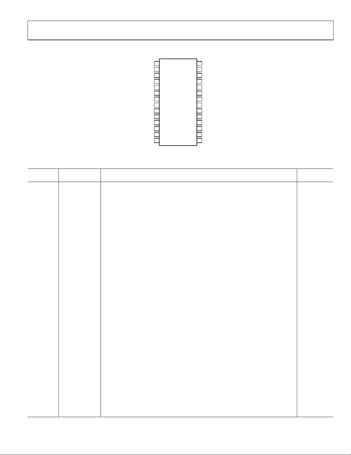
PIN CONFIGURATION AND FUNCTION DESCRIPTIONS
1
LOIP
2
VPOS1
IOPN
IOPP
VCMO
IAIN
COM3
IMXO
COM2
IFIN
IFIP
VPOS2
IOFS
VREF
3
4
5
6
7
8
9
10
11
12
13
14
AD8348
TOP VIEW
(Not to Scale)
Figure 2. 28-Lead TSSOP Pin Configuration
Table 3. Pin Function Descriptions—28-Lead TSSOP
Pin No. Mnemonic Description
1, 28 LOIP, LOIN
LO Inputs. For optimum performance, these inputs should be ac-coupled and driven
differentially. Differential drive from single-ended sources can be achieved via a balun.
To obtain a broadband 50 Ω input impedance, connect a 60.4 Ω shunt resistor between
LOIP and LOIN. Typical input drive level is equal to −10 dBm.
2, 12, 20
3, 4, 25, 26
5 VCMO
VPOS1, VPOS2,
VPOS3
IOPN, IOPP,
QOPP, QOPN
Positive Supply for LO, IF, and Biasing and Baseband Sections, Respectively. These pins
should be decoupled with 0.1 μF and 100 pF capacitors.
I- and Q-Channel Differential Baseband Outputs. Typical output swing is equal to 2 V p-p
differential. The dc common-mode voltage level on these pins is set by the voltage on VCMO.
Baseband DC Common-Mode Voltage. The voltage applied to this pin sets the dc
common-mode levels for all the baseband outputs and inputs (IMXO, QMXO, IOPP, IOPN,
QOPP, QOPN, IAIN, and QAIN). This pin can be connected either to VREF or to a reference
voltage from another device (typically an ADC).
6, 23 IAIN, QAIN
I- and Q-Channel Baseband Amplifier Inputs. The single-ended signals on these pins are
referenced to VCMO and must have a dc bias equal to the dc voltage on the VCMO pin. If
IMXO (QMXO) is dc-coupled to IAIN (QAIN), biasing will be provided by IMXO (QMXO). If
an ac-coupled filter is placed between IMXO and IAIN, these pins can be biased from the
source driving VCMO through a 1 kΩ resistor. The gain from IAIN/QAIN to the differential
outputs (IOPP/IOPN and QOPP/QOPN) is 20 dB.
7, 22 COM3 Ground for Biasing and Baseband Sections.
8, 21 IMXO, QMXO
I- and Q-Channel Mixer Baseband Outputs. These are low impedance (40 Ω) outputs whose
bias levels are set by the voltage applied to the VCMO pin. These pins are typically connected
to IAIN and QAIN, respectively, either directly or through a filter. Each output can drive a
maximum current of 2.5 mA.
9 COM2 IF Section Ground.
10, 11 IFIN, IFIP
IF Inputs. IFIN should be ac-coupled to ground. The single-ended IF input signal should
be ac-coupled into IFIP. The nominal differential input impedance of these pins is 200 Ω.
For a broadband 50 Ω input impedance, a minimum-loss L pad should be used; R
= 57.6 Ω. This provides a 200 Ω source impedance to the IF input. However, the AD8348
R
SHUNT
does not necessarily require a 200 Ω source impedance, and a single shunt 66.7 Ω resistor
can be placed between IFIP and IFIN.
13, 16 IOFS, QOFS
I- and Q-Channel Offset Nulling Inputs. DC offsets on the I-channel mixer output (IMXO)
can be nulled by connecting a 0.1 μF capacitor from IOFS to ground. Driving IOFS with a
fixed voltage (typically a DAC calibrated such that the offset at IOPP/IOPN is nulled) can
extend the operating frequency range to include dc. The QOFS pin can likewise be used
to null offsets on the Q-channel mixer output (QMXO).
14 VREF
Reference Voltage Output. This output voltage (1 V) is the main bias level for the device
and can be used to externally bias the inputs and outputs of the baseband amplifiers.
The typical maximum drive current for this output is 2 mA.
28
27
26
25
24
23
22
21
20
19
18
17
16
15
LOIN
COM1
QOPN
QOPP
ENVG
QAIN
COM3
QMXO
VPOS3
MXIN
MXIP
VGIN
QOFS
ENBL
03678-002
Equivalent
Circuit
A
B
C
D
H
E
= 174 Ω,
SERIES
F
G
Rev. A | Page 7 of 28
Page 8

AD8348
Equivalent
Pin No. Mnemonic Description
15 ENBL Chip Enable Input. Active high. Threshold is equal to VS/2. D
17 VGIN
18, 19 MXIP, MXIN
24 ENVG
27 COM1 LO Section Ground.
Gain Control Input. The voltage on this pin controls the gain on the IF VGA. The gain
control voltage range is from 0.2 V to 1.2 V and corresponds to a conversion gain range
from +25.5 dB to −18.5 dB. This is the gain to the output of the mixers (that is, IMXO and
QMXO). There is an additional 20 dB of fixed gain in the final baseband amplifiers (IAIN to
IOPP/IOPN and QAIN to QOPP/QOPN). Note that the gain control function has a negative
sense (that is, increasing voltage decreases gain).
Auxiliary Mixer Inputs. If ENVG is low, the IFIP and IFIN inputs are disabled and MXIP and
MXIN are enabled, allowing the VGA to be bypassed. The auxiliary mixer inputs are fully
differential inputs that should be ac-coupled to the signal source.
Active High VGA Enable. When ENVG is high, IFIP and IFIN inputs are enabled and MXIP
and MXIN inputs are disabled. When ENVG is low, MXIP and MXIN inputs are enabled and
IFIP and IFIN inputs are disabled.
Circuit
D
I
D
Rev. A | Page 8 of 28
Page 9
AD8348
V
V
V
V
V
V
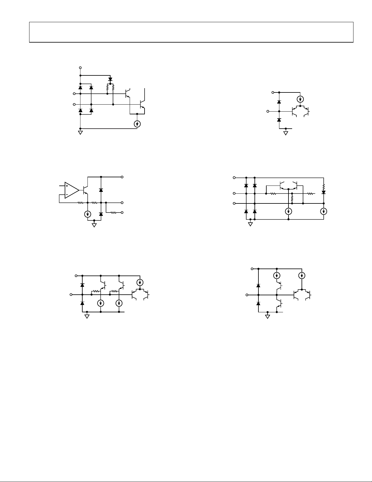
EQUIVALENT CIRCUITS
POS1
LOIN
LOIP
POS3
COM1
Figure 3. Circuit A
COM3
Figure 4. Circuit B
POS3
IOPP, IOPN,
QOPP, QOPN
VCMO
POS3
IAIN, QAIN, VGIN,
ENBL, ENVG
03678-003
COM3
03678-006
Figure 6. Circuit D
POS2
IFIP
IFIN
03678-004
COM3
03678-007
Figure 7. Circuit E
POS3
50µA
MAX
VCMO
COM3
Figure 5. Circuit C
03678-005
Rev. A | Page 9 of 28
IOFS,
QOFS
COM3
Figure 8. Circuit F
03678-008
Page 10

AD8348
V
V
V
POS2
POS3
VREF
COM2
Figure 9. Circuit G
COM3
03678-009
POS3
IMXO,
QMXO
03678-010
MXIP
MXIN
COM3
Figure 11. Circuit I
03678-011
Figure 10. Circuit H
Rev. A | Page 10 of 28
Page 11

AD8348
G
A
G
A
G
A
G
A
G
A
G
A
–
TYPICAL PERFORMANCE CHARACTERISTICS
VGA AND DEMODULATOR
30
25
20
LINERR T = +85°C, V
LINERR T = +25°C, V
LINERR T = –40°C, V
= 5V, FREQ = 380MHz
POS
= 5V, FREQ = 380MHz
POS
= 5V, FREQ = 380MHz
POS
15
10
5
0
AND MIXER GAIN (d B)
–5
V
–10
–15
–20
0.2 0.3 0. 4
T = +85°C, V
= 5V, FREQ = 380MHz
POS
T = +25°C, V
POS
T = –40°C, V
= 5V, FREQ = 380MHz
= 5V, FREQ = 380MHz
POS
0.5 0.6 0. 7 0.8 0.9 1. 0 1.1 1.2
VGIN (V)
Figure 12. Mixer Gain and Linearity Error vs. VGIN, V
= 1 MHz, Temperature = −40°C, +25°C, +85°C
F
BB
4
3
2
1
0
–1
–2
–3
–4
–5
–6
= 5 V, FIF = 380 MHz,
POS
25
20
15
LINERR T = +85°C, V
LINERR T = +25°C, V
LINERR T = –40°C, V
= 2.7V, FREQ = 900MHz
POS
= 2.7V, FREQ = 900MHz
POS
= 2.7V,
POS
FREQ = 900MHz
10
5
0
–5
AND MIXER GAIN (d B)
LINEARITY ERRO R (dB)
–10
V
–15
–20
–25
03678-012
0.2 0.3 0. 4
Figure 15. Mixer Gain and Linearity Error vs. VGIN, V
T = +25°C, V
T = –40°C, V
T = +85°C, V
POS
= 2.7V,
POS
FREQ = 900MHz
= 2.7V, FREQ = 900MHz
= 2.7V, FREQ = 900MHz
POS
0.5 0.6 0. 7 0.8 0.9 1. 0 1.1 1.2
VGIN (V)
= 1 MHz, Temperature = −40°C, +25°C, +85°C
F
BB
= 2.7 V, FIF = 900 MHz,
POS
4
3
2
1
0
–1
–2
–3
LINEARITY ERRO R (dB)
–4
–5
–6
03678-015
25
20
15
LINERR T = +85°C, V
LINERR T = +25°C, V
LINERR T = –40°C, V
= 5V, FREQ = 900MHz
POS
= 5V, FREQ = 900MHz
POS
= 5V,
POS
FREQ = 900MHz
10
5
0
–5
AND MIXER GAIN (d B)
–10
V
–15
–20
–25
0.2 0.3 0. 4
T = +25°C, V
T = –40°C, V
T = +85°C, V
POS
= 5V,
POS
FREQ = 900MHz
= 5V, FREQ = 900MHz
= 5V, FREQ = 900MHz
POS
0.5 0.6 0. 7 0.8 0.9 1. 0 1.1 1.2
VGIN (V)
Figure 13. Mixer Gain and Linearity Error vs. VGIN, V
= 1 MHz, Temperature = −40°C, +25°C, +85°C
F
BB
30
25
20
LINERR T = +85°C, V
LINERR T = +25°C, V
LINERR T = –40°C, V
= 2.7V, FREQ = 380MHz
POS
= 2.7V, FREQ = 380MHz
POS
= 2.7V,
POS
FREQ = 380MHz
15
10
5
0
AND MIXER GAIN (d B)
–5
V
–10
–15
–20
0.2 0.3 0. 4
T = +25°C, V
T = –40°C, V
T = +85°C, V
POS
= 2.7V,
POS
FREQ = 380MHz
= 2.7V, FREQ = 380MHz
= 2.7V, FREQ = 380MHz
POS
0.5 0.6 0. 7 0.8 0.9 1. 0 1.1 1.2
VGIN (V)
Figure 14. Mixer Gain and Linearity Error vs. VGIN, V
= 1 MHz, Temperature = −40°C, +25°C, +85°C
F
BB
4
3
2
1
0
–1
–2
–3
–4
–5
–6
= 5 V, FIF = 900 MHz,
POS
4
3
2
1
0
–1
–2
–3
–4
–5
–6
= 2.7 V, FIF = 380 MHz,
POS
28
26
24
22
AND MIXER GAIN (d B)
LINEARITY ERRO R (dB)
03678-013
V
20
18
100
Figure 16. Gain vs. F
2.7V, 0.2V, +25°C
2.7V, 0.2V, +85°C
5V, 0.2V, –40°C
200 300 400 500 600 700 800 900 1000
IF FREQ UENCY (MHz)
, VGIN = 0.2 V, FBB = 1 MHz,
IF
5V, 0.2V, +25° C
5V, 0.2V, +85°C
2.7V, 0.2V, –40°C
03678-016
Temperature = −40°C, +25°C, +85°C
15
–20
–25
LINEARITY ERRO R (dB)
03678-014
AND MIXER GAIN (d B)
V
–30
100
5V, 1.2V, +85 °C
2.7V, 1.2V, +85 °C
5V, 1.2V, –40°C
2.7V, 1.2V, +25°C
2.7V, 1.2V, –40°C
5V, 1.2V, +25
°C
200 300 400 500 600 700 800 900 1000
IF FREQ UENCY (MHz)
Figure 17. Gain vs. F
, VGIN = 1.2 V, FBB = 1 MHz,
IF
03678-017
Temperature = −40°C, +25°C, +85°C
Rev. A | Page 11 of 28
Page 12

AD8348
G
A
G
A
–
27
26
25
24
23
22
21
AND MIXER GAIN (d B)
20
V
19
18
17
Figure 18. Gain vs. F
5V, 0.2V, +25°C
2.7V, 0.2V, +85°C
2.7V, 0. 2V, +25° C
2.7V, 0.2V, –40°C
5V, 0.2V, +85°C
100
20 30 40 50 60 70 80 90 100
BASEBAND FREQUENCY (M Hz)
, VGIN = 0.2 V, FIF = 380 MHz, V
BB
5V, 0.2V, –40°C
Temperature = −40°C, +25°C, +85°C
= 2.7 V, 5 V,
POS
20
15
10
5
0
+85°C, 5V, 900MHz
–5
–10
–15
–20
INPUT 1dB CO MPRESSIO N POINT ( dBm) (re 200Ω)
03678-018
+25°C, 2.7V, 900MHz
–40°C, 2.7 V, 900MHz
0.4 0.5 0. 6 0.7 0.8 0.9 1.0 1.1 1.2
0.30.2
Figure 21. Input 1 dB Compression Point (IP1dB) vs. VGIN, F
F
= 1 MHz, V
BB
= 2.7 V, 5 V, Temperature = −40°C, +25°C, +85°C
POS
–40°C, 5V, 900MHz
+25°C, 5V, 900MHz
+85°C, 2.7V, 900MHz
VGIN (V)
= 900 MHz,
IF
03678-021
17
–20
–23
AND MIXER GAIN (d B)
V
–26
100
Figure 19. Gain vs. F
Temperature = −40°C, +25°C, +85°C
15
10
5
0
2.7V, 1.2V, +85°C
5V, 1.2V, +85° C
2.7V, 1.2V, +25°C
5V, 1.2V, +25°C
5V, 1.2V, –40°C
2.7V, 1.2V, –40°C
20 30 40 50 60 70 80 90 100
BASEBAND FREQUENCY (M Hz)
, VGIN = 1.2 V, FIF = 380 MHz, V
BB
+25°C, 5V, 380MHz
–40°C, 5V, 380MHz
+25°C, 2. 7V, 380MHz
= 2.7 V, 5 V,
POS
30
29
28
27
2.7V, 1.2V, +85°C
26
INPUT IIP3 (dBm) (re 200Ω)
25
24
03678-019
Figure 22. IIP3 vs. F
2.7V, 1.2V, +25°C
5V, 1.2V, –40°C
2.7V, 1.2V, –40°C
200100
300 400 500 600 700 800 900 1000
IF FREQ UENCY (MHz)
, VGIN = 1.2 V, F
IF
5V, 1.2V, +85°C
5V, 1.2V, +25°C
= 1 MHz, V
BB
= 2.7 V, 5 V,
POS
03678-022
Temperature = −40°C, +25°C, +85°C, Tone Spacing = 20 kHz
0
5V, 0.2V, +85°C
2.7V, 0.2V, +85°C
2.7V, 0.2V, +25°C
–5
–5
–10
+85°C, 5V, 380MHz
–15
–20
–25
INPUT 1dB CO MPRESSIO N POINT ( dBm) (re 200Ω)
–40°C, 2.7 V, 380MHz
0.4 0.5 0. 6 0.7 0.8 0.9 1.0 1.1 1.2
0.30.2
VGIN (V)
Figure 20. Input 1 dB Compression Point (IP1dB) vs. VGIN, F
F
= 1 MHz, V
BB
= 2.7 V, 5 V, Temperature = −40°C, +25°C, +85°C
POS
+85°C, 2.7 V, 380MHz
= 380 MHz,
IF
2.7V, 0.2V, –40°C
= 1 MHz, V
5V, 0.2V, –40°C
= 2.7 V, 5 V,
POS
03678-023
–10
INPUT IIP3 (dBm) (re 200Ω)
–15
03678-020
Figure 23. IIP3 vs. F
100 200
5V, 0.2V, +25°C
300 400 500 600 700 800 900 1000
IF FRE QUENCY (MH z)
, VGIN = 0.2 V, F
IF
BB
Temperature = −40°C, +25°C, +85°C
Rev. A | Page 12 of 28
Page 13

AD8348
G
A
G
A
32
2.7V, 1.2V, +25°C
30
28
26
24
AND MIXER INPUT IIP3 (dBm) (re 200Ω)
V
22
10020
Figure 24. IIP3 vs. F
2.7V, 1.2V, –40°C
5V, 1.2V, –40°C
2.7V, 1.2V, +85°C
5V, 1.2V, +25°C
5V, 1.2V, +85°C
30 40 50 60 70 80 90 100
BASEBAND FREQUENC Y (MHz)
, VGIN = 1.2 V, FIF = 380 MHz, V
BB
Temperature = −40°C, +25°C, +85°C
= 2.7 V, 5 V,
POS
03678-024
45
40
35
30
25
20
15
NOISE FIGURE (dB)
10
5
0
0.2 0.3 0. 4
0.5 0.6 0. 7 0.8 0.9 1. 0 1.1 1.2
VGIN (V)
NF
Figure 27. Noise Figure and IIP3 vs. VGIN, Temperature = 25°C,
F
= 380 MHz, FBB = 1 MHz, V
IF
= 2.7 V
POS
IIP3
35
30
25
20
15
10
5
0
–5
–10
INPUT IIP3 (dBm) (re 200Ω)
03678-027
0
5V, 0.2V, +85°C
–5
–10
2.7V, 0.2V, –40°C
–15
AND MIXER INPUT IIP3 (dBm) (re 200Ω)
V
–20
10020
Figure 25. IIP3 vs. F
16
15
14
13
2.7V, 0.2V, +85°C
5V, 0.2V, +25°C
5V, 0.2V, –40°C
2.7V, 0.2V, +25°C
30 40 50 60 70 80 90 100
BASEBAND FREQUENC Y (MHz)
, VGIN = 0.2 V, FIF = 380 MHz, V
BB
Temperature = −40°C, +25°C, +85°C
NF VGIN = 0.2V
= 2.7 V, 5 V,
POS
40
35
30
25
20
15
NOISE FIGURE (dB)
10
5
0
0.2 0.3 0. 4
03678-025
0.5 0.6 0. 7 0.8 0.9 1. 0 1.1 1.2
VGIN (V)
NF
IIP3
35
30
25
20
15
10
5
0
–5
–10
INPUT IIP3 (dBm) (re 200Ω)
03678-028
Figure 28. Noise Figure and IIP3 vs. VGIN, Temperature = 25°C,
= 380 MHz, FBB = 1 MHz, V
F
IF
16
15
14
13
PHASE ERROR 50MHz PHASE ERRO R 380MHz
NF @ LO = 900MHz
POS
= 5 V
2.0
1.5
1.0
0.5
12
11
NOISE FIGURE (dB)
10
9
8
15050 250
350 450 550 650 750 850 950
Figure 26. Noise Figure vs. F
IF FREQUE NCY (MHz)
, T = 25°C, VGIN = 0.2 V, FBB = 1 MHz
IF
12
11
NOISE FIGURE (dB)
10
9
8
–12 –10
03678-026
PHASE ERROR 900MHz
NF @ LO = 380MHz
NF @ LO = 50MHz
–8 –6 –4 –2 0
LO INPUT LEVEL (V)
Figure 29. Noise Figure and Quadrature Phase Error IMXO/QMXO vs. LO Input
Level, Temperature = 25°C, VGIN = 0.2 V, V
= 5 V for FIF = 50 MHz,
POS
0
–0.5
–1.0
–1.5
–2.0
PHASE ERROR (Degrees)
03678-029
380 MHz, and 900 MHz
Rev. A | Page 13 of 28
Page 14

AD8348
–
DEMODULATOR USING MXIP AND MXIN
11.0
10.5
10.0
TEMP = –40°C, V
TEMP = –40°C, V
POS
= 2.7V
POS
= 5V
18
NF 5V
17
16
15
23.0
22.5
22.0
21.5
TEMP = +25°C,
9.5
9.0
MIXER GAIN ( dB)
8.5
8.0
Figure 30. Mixer Gain vs. F
V
POS
TEMP = +25°C,
100 200
= 5V
= 2.7V
V
POS
TEMP = +85°C, V
300 4 00 500 600 700 800 900 1000
IF FREQ UENCY (MHz)
= 5V
POS
, V
= 2.7 V, 5 V, FBB = 1 MHz,
IF
POS
Temperature = −40°C, +25°C, +85°C
1.5
–2.0
–2.5
–3.0
–3.5
–4.0
–4.5
–5.0
–5.5
–6.0
–6.5
–7.0
MIXER INPUT P1dB (dBm) (re 200Ω)
–7.5
–8.0
TEMP = +85° C, V
TEMP = +85°C, V
100 200
= 5V
POS
= 2.7V
POS
TEMP = + 25°C, V
300 400 500 600 700 800 900 1000
IF FREQ UENCY (MHz)
Figure 31. Input 1 dB Compression Point vs. F
Temperature = −40°C, +25°C, +85°C
TEMP = +85°C,
V
POS
TEMP = +25°C, V
TEMP = –40° C, V
TEMP = –40° C, V
POS
, FBB = 1 MHz, V
IF
= 2.7V
POS
POS
POS
= 2.7V
= 5V
= 5V
= 2.7V
= 2.7 V, 5 V,
POS
14 21.0
IIP3 5V
13
12
INPUT IIP3 (dBm) (re 200Ω)
11
10
03678-030
50 150
IIP3 2.7V
250 350 450 550 650 750 850 950
Figure 32. IIP3 and Noise Figure vs. F
NF 2.7V
IF FREQUENCY (MHz)
, V
= 2.7 V, 5 V, Temperature = 25°C
IF
POS
20.5
20.0
19.5
19.0
NOISE FIGURE (dB)
03670-032
03678-031
Rev. A | Page 14 of 28
Page 15

AD8348
FINAL BASEBAND AMPLIFIERS
21
–40°C, 5V
20
19
18
+85°C, 2.7V
17
GAIN (dB)
16
15
14
13
0.1
Figure 33. Gain vs. F
–40°C, 2.7V
+25°C, 2.7V
+25°C, 5V
1 10 100 1000
BASEBAND FREQUENC Y (MHz)
, V
BB
VCMO
= VREF = 1 V, V
= 2.7 V, 5 V,
POS
Temperature = −40°C, +25°C, +85°C
+85°C, 5V
03678-033
35
30
25
20
15
10
5
–5
–10
–15
+25°C, 2. 7V
0
–40°C, 2.7V
10
OIP3 (dBV)
Figure 35. OIP3 vs. F
–40°C, 5V
+25°C, 5V
+85°C, 5V
+85°C, 2.7V
50 70 9030 130110 150 170 190
BASEBAND FREQUENC Y (MHz)
, V
BB
VCMO
= VREF = 1 V, V
= 2.7 V, 5 V,
POS
Temperature = −40°C, +25°C, +85°C
03678-035
5
+25°C, 5V +85° C, 5V
0
–5
–10
OP1dB (dBV)
–15
–20
0.1
+25°C, 2.7V
–40°C, 2.7V
+85°C, 2.7V
1 10 100 1000
BASEBAND FREQUENC Y (MHz)
Figure 34. OP1dB Compression vs. F
Temperature = −40°C, +25°C, +85°C
–40°C, 5V
, V
BB
VCMO
= VREF = 1 V, V
= 2.7 V, 5 V,
POS
10
9
8
7
6
5
4
3
2
SPECTRAL DENSITY (nV/ Hz)
BASEBAND AMPLIF IER INPUT NOISE
1
0
03678-034
1
10 1 00 1000 10000 100000
FREQUENCY (kHz)
03678-036
Figure 36. Noise Spectral Density
Rev. A | Page 15 of 28
Page 16

AD8348
A
A
A
A
VGA/DEMODULATOR AND BASEBAND AMPLIFIER
2.0
2.0
1.5
1.0
2.7V, 0.2V, –40°C
0.5
0
–0.5
TURE PHASE ERROR ( Degrees)
–1.0
–1.5
QUADR
–2.0
5V, 0.2V, +25°C
100
2.7V, 0.2V, +85°C
200 300 40 0 50 0 600 700 800 900 1000
IF FREQ UENCY (MHz)
Figure 37. Quadrature Phase Error vs. F
Temperature = −40°C, +25°C, +85°C
2.0
2.7V, 0.7V, +25°C
2.7V, 0.7V, –40°C
5V, 0.7V, –40°C
5V, 0.7V, +25°C
2.7V, 0.7V, +85°C
50 10152025303540
BASEBAND FREQUENC Y (MHz)
–0.5
TURE PHASE ERROR ( Degrees)
–1.0
–1.5
QUADR
–2.0
1.5
1.0
0.5
0
Figure 38. Quadrature Phase Error vs. F
Temperature = −40°C, +25°C, +85°C, F
5V, 0.2V, +85°C
5V, 0.2V, –40°C
2.7V, 0.2V, +25°C
, VGIN = 0.7 V, V
IF
5V, 0.7V, +85°C
, VGIN = 0.7 V, V
BB
= 380 MHz
IF
= 2.7 V, 5 V,
POS
= 2.7 V, 5 V,
POS
1.5
1.0
0.5
TCH (dB)
0
–0.5
–1.0
I/Q AMPLITUDE MISM
–1.5
–2.0
03678-037
Figure 40. I/Q Amplitude Imbalance vs. F
300
280
260
240
220
200
180
160
SHUNT RESISTANCE (Ω)
140
120
100
03678-038
50 150 250
Figure 41. Input Impedance of IF Input vs. F
200100 300 400 500 600 700 800 900 1000
IF FREQ UENCY (MHz)
, Temperature = 25°C, V
IF
SHUNT CAPACITANCE
SHUNT RESISTANCE
350 450 550 650 750 850 950
IF FREQ UENCY (MHz)
, VGIN = 0.7 V, V
IF
POS
POS
2.2
2.0
1.8
1.6
1.4
1.2
1.0
0.8
0.6
0.4
0.2
= 5 V
= 5 V
03678-040
SHUNT CAPACITANCE (pF)
03678-041
90
60
300
30
330
0180
03678-042
0.4
0.2
TCH (dB)
5V, 0.7V, 25°C
BASEBAND FREQUENC Y (MHz)
I/Q AMPLITUDE MISM
–0.2
–0.4
0
50 10152025303540
Figure 39. I/Q Amplitude Imbalance vs. F
, Temperature = 25°C, V
BB
POS
03678-039
= 5 V
120
150
IFIP WITH L PAD
210
240
Figure 42. S11 of IF Input vs. F
= 5 V (with L Pad, with No Pad, Normalized to 50 Ω)
V
POS
IFIP WITHOUTL PAD
IMPEDANCE CIRCLE
270
, FIF = 50 MHz to 1 GHz, VGIN = 0.7 V,
IF
Rev. A | Page 16 of 28
Page 17

AD8348
300
280
260
240
220
200
180
160
SHUNT RESISTANCE (Ω)
140
120
100
50
100
(SHUNT CAPACITANCE)
150
200
250
300
(SHUNT RESIS TANCE)
350
400
450
550
500
IF FREQ UENCY (MHz)
600
Figure 43. Input Impedance of Mixer Input vs. F
90
650
750
700
, VGIN = 0.7 V, V
IF
800
850
900
950
2.5
2.0
1.5
1.0
0.5
0
1000
POS
= 5 V
SHUNT CAPACITANCE (pF)
03678-043
0
–5
–10
–15
–20
RETURN LOSS (d B)
–25
–30
–35
200
100
RETURN LOSS LO INPUT, THROUGH BALUN
WITH 60.4Ω IN SHUNT BETWEEN LO IP/LO IN
400
500
300
600
700
800
900
1100
1000
1200
1300
FREQUENCY APPLIED TO LOIP /LOIN (M Hz)
1400
1500
1600
Figure 46. Return Loss of LO Input vs. External LO Frequency
Through Balun, with Termination Resistor
1700
1800
1900
2000
03678-046
120
150
MX INPUTS WITH 4:1 BALUN
210
240
IMPEDANCE CIRCL E
Figure 44. S11 of Mixer Input vs. F
VGIN = 0.7 V, V
0
–5
–10
–15
RETURN LOSS LOIP PIN SINGLE-ENDED,
= 5 V (With and Without Balun)
POS
LOIN AC-COUPLED TO GROUND.
MXIP INPUT PIN
270
, FIF = 50 MHz to 1 GHz,
IF
60
300
30
330
65
60
55
0180
50
45
SUPPLY CURRENT (mA)
40
35
03678-044
VS = 5V
–30–40 –20 –10 0 10 2 0 30 40 50 60 70 80
TEMPERATURE (°C)
V
S
= 2.7V
03678-047
Figure 47. Supply Current vs. Temperature
–20
RETURN LOSS (d B)
–25
–30
–35
400
500
200
100
300
600
700
800
900
1200
1300
1400
1500
1600
1100
EXTERNAL L O FREQUENCY (MHz)
1000
1700
Figure 45. Return Loss of LOIP Input vs. External LO Frequency
1800
1900
2000
03678-045
Rev. A | Page 17 of 28
Page 18

AD8348
O
V
THEORY OF OPERATION
REF
BIAS
ENBL
VGIN
IFIP
IFIN
15
11
10
17
CELL
GAIN
CONTROL
VREF
18 2419 21 16 23 25 26
Figure 48. Functional Block Diagram
VGA
The VGA is implemented using the patented X-AMP architecture.
The single-ended IF signal is attenuated in eight discrete 6 dB
steps by a passive R-2R ladder. Each discrete attenuated version
of the IF signal is applied to the input of a transconductance
stage. The current outputs of all transconductance stages are
summed together and drive a resistive load at the output of the
VGA. Gain control is achieved by smoothly turning on and
off the relevant transconductance stages with a temperaturecompensated interpolation circuit. This scheme allows the gain
to continuously vary over a 44 dB range with linear-in-decibel
gain control. This configuration also keeps the relative dynamic
range constant (for example, IIP3 − NF in dB) over the gain
setting; however, the absolute intermodulation intercepts and
noise figure vary directly with gain. The analog voltage VGIN
sets the gain. VGIN = 0.2 V is the maximum gain setting, and
VGIN = 1.2 V is the minimum voltage gain setting.
DOWNCONVERSION MIXERS
The output of the VGA drives two (I and Q) double-balanced
Gilbert cell downconversion mixers. Alternatively, driving the
ENVG pin low can disable the VGA, and the mixers can be
externally driven directly via the MXIP and MXIN ports. At
the input of the mixer, a degenerated differential pair performs
linear voltage-to-current conversions. The differential output
current feeds into the mixer core where it is downconverted by
the mixing action of the Gilbert cell. The phase splitter provides
quadrature LO signals that drive the LO ports of the in-phase
and quadrature mixers.
Buffers at the output of each mixer drive the IMXO and QMXO
pins. These linear, low output impedance buffers drive 40 Ω,
temperature-stable, passive resistors in series with each output
pin (IMXO and QMXO). This 40 Ω should be considered when
calculating the reverse termination if an external filter is inserted
between IMXO (QMXO) and IAIN (QAIN). The VCMO pin sets
the dc output level of the buffer. This can be set externally or
connected to the on-chip 1.0 V reference, VREF.
IOFSIAIN IOPP IOPN
IMX
DIVIDE
BY 2
PHASE
SPLITTER
VCMO
QOFSENVG QXMOMXINMXIP QAIN QOPP QOPN
VCMO
AD8348
34613814
5
VCMO
1
LOIP
28
LOIN
PHASE SPLITTER
Quadrature generation is achieved using a divide-by-2 frequency
divider. Unlike a polyphase filter that achieves quadrature over
a limited frequency range, the divide-by-2 approach maintains
quadrature over a broad frequency range and does not attenuate
the LO. The user, however, must provide an external signal XLO
that is twice the frequency of the desired LO frequency. XLO drives
the clock inputs of two flip-flops that divide down the frequency
by a factor of 2. The outputs of the two flip-flops are one-half
03678-049
period of XLO out of phase. Equivalently, the outputs are onequarter period (90°) of the desired LO frequency out of phase.
Because the transitions on XLO define the phase difference at
the outputs, deviation from 50% duty cycle translates directly to
quadrature phase errors.
If the user generates XLO from a 1× frequency (f
frequency-doubling circuit (XLO = 2 × f
there is a 180° phase uncertainty between f
), fundamentally
REF
REF
) and a
REF
and the AD8348
internal quadrature LO. The phase relationship between I and Q
LO, however, is always 90°.
I/Q BASEBAND AMPLIFIERS
Two (I and Q) fixed gain (20 dB), single-ended-to-differential
amplifiers are provided to amplify the demodulated signal
after off-chip filtering. The amplifiers use voltage feedback to
linearize the gain over the demodulation bandwidth. These
amplifiers can be used to maximize the dynamic range at the
input of an ADC following the AD8348.
The input to the baseband amplifiers, IAIN (QAIN), feeds into
the base of a bipolar transistor with an input impedance of
roughly 50 kΩ. The baseband amplifiers sense the single-ended
difference between IAIN (QAIN) and VCMO. IAIN (QAIN)
can be dc biased by terminating it with a shunt resistor to
VCMO, such as when an external filter is inserted between
IMXO (QMXO) and IAIN (QAIN). Alternatively, any dc
connection to IMXO (QXMO) can provide appropriate bias via
the offset-nulling loop.
ENABLE
A master biasing cell that can be disabled using the ENBL pin
controls the biasing for the chip. If the ENBL pin is held low,
the entire chip powers down to a low power sleep mode,
typically consuming 75 µA at 5 V.
BASEBAND OFFSET CANCELLATION
A low output current integrator senses the output voltage offset
at IOPP and IOPN (QOPP and QOPN) and injects a nulling
current into the signal path. The integration time constant of the
offset-nulling loop is set by Capacitor COFS from IOFS (QOFS) to
Rev. A | Page 18 of 28
Page 19

AD8348
VCMO. This forms a high-pass response for the baseband
signal path with a lower 3 dB frequency of
f
PASS
1
×Ω×π=26502
COFS
Alternatively, the user can externally adjust the dc offset by driving
IOFS (QOFS) with a digital-to-analog converter or other voltage
source. In this case, the baseband circuit operates all the way down
to dc (f
= 0 Hz). The integrator output current is only 50 µA
PASS
and can be easily overridden with an external voltage source.
The nominal voltage level applied to IOFS (QOFS) to produce
a 0 V differential offset at the baseband outputs is 900 mV.
The IOFS (QOFS) pin must be connected to either a bypass
capacitor (>0.1 µF) or an external voltage source to prevent the
feedback loop from oscillating.
The feedback loop will be broken at dc if an ac-coupled baseband
filter is placed between the mixer outputs and the baseband
amplifier inputs. If an ac-coupled filter is implemented, the user
must handle the offset compensation via some external means.
Rev. A | Page 19 of 28
Page 20

AD8348
N
APPLICATIONS
BASIC CONNECTIONS
Figure 49 shows the basic connections schematic for the AD8348.
J21
LO
+V
IOP
IOPP
S
J3I
J2I
R31
57.6Ω
IFIP
+V
S
C52
0.1µF
0.1µF
C51
100pF
V
REF
C32
1000pF
R32
174Ω
C31
1000pF
C53
C54
100pF
C0l
0.1µF
C11
4.7µF
Figure 49. Basic Connections Schematic
POWER SUPPLY
The voltage supply for the AD8348, between 2.7 V and 5 V, should
be provided to the +VPOSx pins, and ground should be connected
to the COMx pins. Each supply pin should be decoupled separately
using two capacitors whose recommended values are 100 pF and
0.1 F (values close to these can also be used).
DEVICE ENABLE
To enable the device, the ENBL pin should be driven to VS.
Grounding the ENBL pin disables the device.
VGA ENABLE
Driving the voltage on the ENVG pin to VS enables the VGA. In
this mode, the MX inputs are disabled and the IF inputs are
used. Grounding the ENVG pin disables the VGA and the IF
inputs. When the VGA is disabled, the MX inputs should be used.
GAIN CONTROL
When the VGA is enabled, the voltage applied to the VGIN pin sets
the gain. The gain control voltage range is between 0.2 V and 1.2 V.
This corresponds to a gain range between +25.5 dB and −18.5 dB.
LO INPUTS
For optimum performance, the local oscillator port should be
driven differentially through a balun. The recommended balun
is M/A-COM ETC1-1-13. The LO inputs to the device should
be ac-coupled, unless an ac-coupled transformer is being used.
For a broadband match to a 50 Ω source, a 60.4 Ω resistor
should be placed between the LOIP and LION pins.
1000pF
C21
AD8348
1
2
VPOS1 COM1
3
IOPN QOPN
4
IOPP QOPP
5
VCMO ENVG
IAIN QAIN
6
COM3 COM3
7
IMXO QMXO
8
COM2 VPOS3
9
IFIN MXIN
10
IFIP MXIP
11
VPOS2 VGIN
12
13
IOFS QOFS
VREF ENBL
14
R21
60.4Ω
54
T21
ETC1-1-13
13
LOINLOIP
C22
1000pF
28
27
26
25
24
23
22
21
20
19
18
17
16
15
J3Q
QOPN
J2Q
IF
SW12
MX
C56
C55
+V
0.1µF
100pF
C41
1µF
C0Q
0.1µF
VGIN
S
ETK4-2T
ENBL
SW11
DENBL
1000pF
T41
1000pF
C43
C42
QOPP
+V
S
R42
0Ω
MXIP
+V
S
LO
45
ETC1-1-13
1000pF 1000pF
31
60.4Ω
1
LOIP LOIN
28
03678-050
Figure 50. Differential LO Drive with Balun
Alternatively, the LO port can be driven from a single-ended source
without a balun (
Figure 51). The LO signal is ac-coupled directly
into the LOIP pin via an ac-coupling capacitor, and the LOIN pin
is ac-coupled to ground. Driving the LO port from a singleended source results in an increase in both quadrature phase
error and LO leakage.
LO
1000pF 1000pF
60.4Ω
1
03678-064
LOIP LOIN
28
03678-051
Figure 51. Single-Ended LO Drive
The recommended LO drive level is between −12 dBm and
0 dBm. The LO frequency at the input to the device should be
twice that of the desired LO frequency at the mixer core. The
applied LO frequency range is between 100 MHz and 2 GHz.
IF INPUTS
The IF inputs have an input impedance of 200 Ω. A broadband
50 Ω match can be presented to the driving source through the use
of a minimum-loss L pad. This minimum-loss pad introduces
an 11.46 dB loss in the input path and must be taken into account
when calculating metrics such as gain and noise figure.
Figure 42
shows the S11 of the IF input with and without the L pad.
1000pF
10
IFIN
57.6Ω
IFIP IFIP
174Ω
Figure 52. Minimum-Loss L Pad for 50 Ω IF Input
1000pF
11
03678-052
MX INPUTS
The mixer inputs, MXIP and MXIN, have a nominal impedance
of 200 Ω and should be driven differentially. When driven from
a differential source, the input should be ac-coupled to the
source via capacitors, as shown in
Figure 53.
Rev. A | Page 20 of 28
Page 21

AD8348
O
Z
1000pF
19
18
MXIP MXIP
1000pF
MXINMXIN
03678-053
Figure 53. Driving the MX Inputs from a Differential Source
If the MX inputs are to be driven from a single-ended 50 Ω source,
a 4:1 balun can be used to transform the 200 Ω impedance of
the inputs to 50 Ω while performing the required single-endedto-differential conversion. The recommended transformer is the
M/A-COM ETK4-2T.
MXIN
19
1µF
MXIP
18
Figure 54. Driving the MX Inputs from a Single-Ended 50 Ω Source
1000pF
ETK4-2T
1000pF
MXIP
03678-066
BASEBAND OUTPUTS
The baseband amplifier outputs, IOPP, IOPN, QOPP, and QOPN,
should be presented with loads of at least 2 kΩ (single-ended to
ground). They are not designed to drive 50 Ω loads directly. The
typical swing for these outputs is 2 V p-p differential (1 V p-p
single-ended), but larger swings are possible as long as care is taken
to ensure that the signals remain within the lower limit of 0.5 V
and the upper limit of V
− 1 V of the output swing. To achieve
S
a larger swing, it is necessary to adjust the common-mode bias of
the baseband output signals. Increasing the swing can have the
benefit of improving the signal-to-noise ratio of the baseband
amplifier output.
When connecting the baseband outputs to other devices, care
should be taken to ensure that the outputs are not capacitively
loaded by approximately 20 pF or more. Such loads could
potentially overload the output or induce oscillations. The effect
of capacitive loading on the baseband amplifier outputs can be
mitigated by inserting series resistors of approximately 200 Ω.
OUTPUT DC BIAS LEVEL
The dc bias of the mixer outputs and the baseband amplifier
inputs and outputs is determined by the voltage that is driven
onto the VCMO pin. The range of this voltage is typically
between 500 mV and 4 V when operating with a 5 V supply.
To achieve maximum voltage swing from the baseband amplifiers,
VCMO should be driven at 2.25 V; this allows a swing of up to
7 V p-p differential (3.5 V p-p single-ended).
INTERFACING TO DETECTOR FOR AGC OPERATION
The AD8348 can be interfaced with a detector such as the
AD8362 rms-to-dc converter to provide an automatic signalleveling function for the baseband outputs.
+V
IF INPUT
= 200Ω
O
S
L
1000pF 1000pF
100pF0.1µF
TO BASEBAND
I ADC
V
REF
1.02kΩ 1.24kΩ
1000pF
+V
S
0.1µF 100pF
V
REF
1000pF
100pF
1000pF
60.4Ω
AD8348
1
2
VPOS1 COM1
3
IOPN QOPN
4
IOPP QOPP
5
VCMO ENVG
IAIN QAIN
6
7
COM3 COM3
IMXO QMXO
8
COM2 VPOS3
9
IFIN MXIN
10
IFIP MXIP
11
VPOS2 VGIN
12
13
IOFS QOFS
VREF ENBL
14
54
1:1
13
28
LOINLOIP
27
26
25
+V
24
S
23
22
21
20
19
1000pF
18
1000pF
17
16
15
100pF
100pF
TO BASEBAND
0.1µF100pF
+V
S
Q ADC
V
CMO
+V
S
AD8362
1
ACOMCOMM
1µF
1µF
1µF
1µF
2
3
4
5
6
7
8
16
VREFCHPF
15
VTGTDECL
14
VPOSINHI
13
100pF 0.1µF
VOUTINLO
12
VSETDECL
11
ACOMPWDN
10
9
CLPFCOMM
V
1µF
+V
S
SET
Figure 55. AD8362 Configuration for AGC Operation
Assuming the I and Q channels have the same rms power, the
mixer output (or the output of the baseband filter) of one channel
can be used as the input of the AD8362. The AD8362 should be
operated in a region where its linearity error is small. Also, a
voltage divider should be implemented with an external resistor
in series with the 200 Ω input impedance of the AD8362 input.
This attenuates the AD8348 mixer output so that the AD8362
input is not overdriven. The size of the resistor between the
mixer output and the AD8362 input should be chosen so that
the peak signal level at the input of the AD8362 is about 10 dB
less than the approximately 10 dBm maximum of the AD8362
dynamic range.
The other side of the AD8348 baseband output should be
loaded with a resistance equal to the series resistance of the
attenuating resistor in series with the AD8362’s 200 Ω input
impedance. This resistor should be tied to the source driving
VCMO so that there is no dc drawn from the mixer output.
03678-0-055
Rev. A | Page 21 of 28
Page 22

AD8348
T
A
A
A
The level of the mixer output (or the output of the baseband
filter) can then be set by varying the setpoint voltage fed to
Pin 11 (VSET) of the AD8362.
Care should be taken to ensure that blockers—unwanted signals
in the band of interest that are demodulated along with the desired
signal—do not dominate the rms power of the AD8362 input.
This can cause an undesired reduction in the level of the mixer
output. To overcome this, baseband filtering can be implemented
to filter out undesired signals before the signal is presented to
the AD8362.
Figure 56 shows the effectiveness of the AGC loop in
maintaining a baseband amplifier output amplitude with less
than 0.5 dB of amplitude error over an IF input range of 40 dB
while demodulating a QPSK-modulated signal at 380 MHz.
The AD8362 is insensitive to crest factor variations and
therefore provides similar performance regardless of the
modulation of the incoming signal.
QPSK
3
2
1
0
–1
ERROR (d B)
–2
–3
–4
AGE OUTPUT
(IOPP – IOPN) (mV rms)
I CHANNEL VOL
140
130
120
110
100
90
80
70
–55 –45
IFIP POWER INPUT (dBm, ZO = 200Ω)
–5.1dBm re 10kΩ
ERROR
–35 –25 –15 –5 5
Figure 56. AD8348 Baseband Amplifier Output vs.
IF Input Power with AD8362 AGC Loop
BASEBAND FILTERS
Baseband low-pass or band-pass filtering can be conveniently
performed between the mixer outputs (IMXO and QMXO) and
the input to the baseband amplifiers. Consideration should be
given to the output impedance of the mixers (40 Ω).
C1
4.7pFC28.2pF
Figure 57 shows the schematic for a 100 Ω, fourth-order elliptic
low-pass filter with a 3 dB cutoff frequency of 20 MHz. Source
and load impedances of approximately 100 Ω ensure that the
filter sees a matched source and load. This also ensures that the
mixer output is driving an overall load of 200 Ω. Note that the
shunt termination resistor is tied to the source driving VCMO
and not to ground. This ensures that the input to the baseband
amplifier is biased to the proper reference level. VCMO is not
an output pin and must be biased by a low impedance source.
The frequency response and group delay of this filter are shown
in
Figure 58 and Figure 59.
0
–10
–20
–30
–40
TION (dB)
–50
TTENU
–60
–70
–80
1
Figure 58. Baseband Filter Response
50
45
40
03678-065
35
30
Y (ns)
25
1
20
15
GROUP DEL
10
5
0
1
Figure 59. Baseband Filter Group Delay
10 100
FREQUENCY (MHz)
2
10 1 00
FREQUENCY ( MHz)
03678-057
03678-058
R1
60Ω
0.68µH
IMXO VCMO IAIN
L2
L1
1.2µH
C5
150pFC682pFR2100Ω
AD8348
TO AD8362
INPUT IF AGC
LOOP IS USED
03678-056
Figure 57. Baseband Filter Schematic
Rev. A | Page 22 of 28
Page 23

AD8348
LO GENERATION
Analog Devices has a line of PLLs that can be used for
generating the LO signal.
Tabl e 4 lists the PLLs and their
maximum frequency and phase noise performance.
Table 4. ADI PLL Selection Table
@ 1 kHz ΦN
Frequency F
ADI Model
ADF4001BRU 165 −99
ADF4001BCP 165 −99
ADF4110BRU 550 −91
ADF4110BCP 550 −91
ADF4111BRU 1200 −78
ADF4111BCP 1200 −78
ADF4112BRU 3000 −86
ADF4112BCP 3000 −86
ADF4116BRU 550 −89
ADF4117BRU 1200 −87
ADF4118BRU 3000 −90
(MHz)
IN
dBc/Hz,
200 kHz PFD
ADI also offers the ADF4360 fully integrated synthesizer and
VCO on a single chip that offers differential outputs for driving
the local oscillator input of the AD8348. This means that the user
can eliminate the use of a balun for single-ended-to-differential
conversions. The ADF4360 comes as a family of chips with six
operating frequency ranges. One can be chosen depending on
the local oscillator frequency required.
Table 5 shows the
options available.
Table 5. ADF4360 Family Operating Frequencies
ADI Model Output Frequency Range (MHz)
ADF4360-1 2150 to 2450
ADF4360-2 1800 to 2150
ADF4360-3 1550 to 1950
ADF4360-4 1400 to 1800
ADF4360-5 1150 to 1400
ADF4360-6 1000 to 1250
ADF4360-7 Lower frequencies set by external L
EVALUATION BOARD
Figure 60 shows the schematic for the AD8348 evaluation
board. Note that uninstalled components are indicated with the
OPEN designation. The board is powered by a single supply in
the range of 2.7 V to 5.5 V.
ration options of the evaluation board.
jumper configurations for operating the evaluation board with
different signal paths.
Power to operate the board can be fed to a single V
located near the LO input port at the top of the evaluation
board. A GND test point is conveniently provided next to the
V
test point for the return path.
S
Tabl e 6 details the various configu-
Tabl e 7 shows the various
test point
S
The device is enabled by moving Switch SW11 (at the bottom left
of the evaluation board) to the ENBL position. The device is
disabled by moving SW11 to the DENBL position. If desired, the
device can be enabled and disabled from an external source that
can be fed into the ENBL SMA connector or the VENB test point,
in which case SW11 should be placed in the DENBL position.
The IF and MX inputs are selected via SW12. The switch should
be moved in the direction of the desired input.
Gain Control
For convenience, a potentiometer, R15, is provided to allow for
changes in gain without the need for an additional dc voltage
source. To use the potentiometer, the SW13 switch must be set
to the POT position. Alternatively, an external voltage applied
to either the test point or SMA connector labeled VGIN can set
the gain. SW13 must be set to the EXT position when an
external gain control voltage is used.
LO Input
The local oscillator signal should be fed to the SMA Connector
J21. This port is terminated in 50 Ω. The acceptable LO power
input range is from −12 dBm to 0 dBm and must be at a
frequency double that of the IF/MX frequency. Remember that
the AD8348 uses a 2:1 frequency divider in the LO path to
generate the internally required quadrature-phase-related LO
signals.
IF Input
The IF input should be fed into the SMA connector IFIP. The
VGA must be enabled when this port is used (SW12 in the IF
position). When this IF input is chosen, the signal path includes
a minimum-loss attenuator to transform a 50 Ω input source to
the 200 Ω source impedance level for which the VGA was
designed. This pad provides a very broadband input match at
the expense of an 11.46 dB power attenuation in the input path.
It is very important to take this into account when measuring
the noise and distortion performance of the unmodified board
using the IFIP input; the apparent noise figure will be degraded
by 11.46 dB, and the apparent IIP3 will be 11.46 dB higher than
actual. If full weak-signal performance is desired from the
evaluation board, the attenuator (comprising R31 and R32)
should be removed and replaced with a low-loss RF transformer
providing the desired 4:1 impedance ratio. When a transformer
is used, IFIN should be ac-coupled to ground and not driven
differentially with IFIP.
MX Input
The evaluation board is by default set for a differential MX drive
through a balun (T41) from a single-ended source fed into the
MXIP SMA connector. When the MX inputs are used, the
internal VGA is bypassed. To change to a differential driving
source, T41 should be removed along with Resistor R42. The
0 Ω R43 and R44 resistors should be installed in place of T41 to
bridge the gap between the input traces. This presents a nominal
Rev. A | Page 23 of 28
Page 24

AD8348
differential impedance of 200 Ω (100 Ω per side). The
differential inputs should then be fed into SMA connectors
MXIP and MXIN.
Mixer Outputs
The I and Q mixer outputs are available through the IMXO and
QMXO SMA connectors. These outputs are biased to VCMO
and are not designed to drive loads smaller than 200 Ω. To
prevent damage to test equipment that cannot tolerate dc biases,
pads for series dc-blocking capacitors are provided. These pads
are populated with 0 Ω by default.
Baseband Outputs
The baseband outputs are made available at the IOPP, IOPN,
QOPP, and QOPN test points and SMA connectors. These
outputs are not designed to be connected directly to 50 Ω loads
and should be presented with loads of approximately 2 kΩ or
greater.
The dc bias level of the baseband amplifier outputs are by
default tied to VREF through LK11. If desired, the dc bias level
can be changed by removing LK11 and driving a dc voltage
onto the VCMO test point.
J3I
IOPN
J2I
IOPP
J1I
IMXO
R2I
OPEN
IFIP
ENBL
LK2I
C7I
OPEN
VCMO
IOPN
GND
IOPP
C10I
0Ω
VENB
+V
VCMO
IMXO
L3I
OPEN
C3I
OPEN
OPEN
R12
10kΩ
S
C6I
57.6Ω
+V
ENBL
OPEN
OPEN
R31
S
C9I
C8I
C52
0.1µF
L2I
OPEN
C2I
OPEN
OPEN
R32
174Ω
SW11
DENBL
C5I
1000pF
1000pF
C54
0.1µF
C13
0.1µF
C32
C31
R11
49.9Ω
C51
100pF
R5I
0Ω
R4I
0Ω
L1I
OPEN
C1I
OPEN
OPEN
J21
LO
C21
1000pF
1
2
3
R3I
49.9Ω
LK4I
LK3I
LK1I
R1I
C4I
OPEN
C53
LK5I LK5Q
100pF
IOFS QOFS
C0I
0.1µF
4
5
LK11
6
7
8
9
10
11
12
13
14
VREF
54
ETC1-1-13
13
R21
60.4Ω
AD8348
LOINLOIP
VPOS1 COM1
IOPN QOPN
IOPP QOPP
VCMO ENVG
IAIN QAIN
COM3 COM3
IMXO QMXO
COM2 VPOS3
IFIN MXIN
IFIP MXIP
VPOS2 VGIN
IOFS QOFS
VREF ENBL
C11
4.7µF
T21
Figure 60. Evaluation Board Schematic
C22
1000pF
28
27
26
25
24
23
22
21
20
19
18
17
16
15
LK4Q
LK3Q
LK1Q
OPEN
R1Q
R3Q
49.9Ω
C0Q
0.1µF
L1Q
OPEN
C1Q
OPEN
C4Q
OPEN
C55
100pF
R5Q
0Ω
R4Q
0Ω
+V
GND
+V
VCMO
C55
0.1µF
S
S
C9Q
OPEN
C8Q
OPEN
IF MX
L2Q
OPEN
C2Q
OPEN
C5Q
OPEN
+V
S
C41
1µF
R14
10kΩ
POT
SW13
EXT
QMXO
OPEN
OPEN
C6Q
OPEN
R44
OPEN
R43
OPEN
SW12
L3Q
C3Q
R13
OPEN
QOPN
GND
QOPP
C10Q
0Ω
ETK4-2T
C7Q
OPEN
C43
1000pF
T41
C42
1000pF
C12
0.1µF
LK2Q
J3Q
QOPN
J2Q
QOPP
J1Q
QMXO
R2Q
OPEN
VCMO
R42
0Ω
R41
OPEN
R15
10kΩ
POT
VGIN
MXIN
MXIP
03678-059
Rev. A | Page 24 of 28
Page 25

AD8348
Figure 61. Evaluation Board Top Layer
03678-060
Figure 62. Evaluation Board Top Silkscreen
Rev. A | Page 25 of 28
03678-061
Page 26

AD8348
Figure 63. Evaluation Board Bottom Layer
03678-062
Figure 64. Evaluation Board Bottom Silkscreen
03678-063
Rev. A | Page 26 of 28
Page 27

AD8348
Table 6. Evaluation Board Configuration Options
Component Function Default Condition
VS, GND Power supply and ground vector pins. Not applicable
SW11, ENBL
Device enable: Place SW11 in the ENBL position to connect the ENBL pin to V
. Place SW11 in
S
the DENBL position to disable the device by grounding the Pin ENBL through a 50 Ω pull-down
resistor. The device can also be enabled via an external voltage applied to ENBL or VENB.
SW13, R15,
VGIN
Gain control selection: With SW13 in the POT position, the gain of the VGA can be set using the
R15 potentiometer. With SW13 in the EXT position, the VGA gain can be set by an external
voltage to the SMA connector VGIN. For VGA operation, the VGA must first be enabled by
setting SW12 to the IF position.
SW12
VGA enable selection: With SW12 in the IF position, the ENVG pin is connected to V
and the
S
VGA is enabled. The IF input should be used when SW12 is in the IF position. With SW12 in the
MX position, the ENVG pin is grounded and the VGA is disabled. The MX inputs should be used
when SW12 is in the MX position.
IFIP, R31, R32
IF inputs: The single-ended IF signal should be connected to this SMA connector. R31 and R32
form an L pad that presents a 50 Ω termination to the driving source. This L pad introduces an
11.46 dB loss in the input signal path and should be taken into consideration when calculating
the gain of the AD8348.
MXIP, MXIN,
T41,
R41, R42,
C42, C43
Mixer inputs: These inputs can be configured for either differential or single-ended operation.
The evaluation board is by default set for differential MX drive through a balun (T41) from a
single-ended source fed into the MXIP SMA connector. To change to a differential driving source,
T41 should be removed along with Resistor R42. The 0 Ω Resistors R43 and R44 should be installed in
place of T41 to bridge the gap between the input traces. This will present a nominal differential
impedance of 200 Ω (100 Ω per side). The differential inputs should then be fed into SMA
connectors MXIP and MXIN.
LK11, VCMO
Baseband amplifier output bias: Installing LK11 connects VREF to VCMO. This sets the bias level
on the baseband amplifiers to VREF, which is equal to approximately 1 V. Alternatively, with
LK11 removed, the bias level of the baseband amplifiers can be set by applying an external
voltage to the VCMO test point.
C8, C9, R4, R5
(I and Q)
C10 (I and Q)
Baseband amplifier outputs and output filter: Additional low-pass filtering can be provided at
the baseband output with these filters.
Mixer output dc-blocking capacitors: The mixer outputs are biased to VCMO. To prevent
damage to test equipment that cannot tolerate dc biases, C10 is provided to block the dc
component, thus protecting the test equipment.
C1 to C7,
R1, R2,
L1 to L3
Baseband filter: These components are provided for baseband filtering between the mixer
outputs and the baseband amplifier inputs. The baseband amplifier input impedance is high
and the filter termination impedance is set by R2. See Table 7 for the jumper settings.
(I and Q)
LK5 (I and Q)
Offset compensation loop disable: Installing these jumpers will disable the offset compensation
loop for the corresponding channel.
Table 7. Filter-Jumper Configuration Options
Condition LK1x LK2x LK3x LK4x
xMXO to xAIN Directly
xMXO to xAIN via Filter
xMXO to J1x Directly, xAIN Unused
xMXO to J1x via Filter, xAIN Unused
•
•
• •
•
Drive xAIN from J1x
SW11 = ENBL
SW13 = POT
SW12 = IF
R31 = 57.6 Ω
R32 = 174 Ω
T41 = M/A-COM ETK4-2T;
R41= OPEN; C42, C43 =
1000 pF; R42 = 0 Ω
LK11 installed
R4, R5 = 0 Ω
C10 = 0 Ω
All = OPEN
LK5x = OPEN
•
•
•
•
Rev. A | Page 27 of 28
Page 28

AD8348
OUTLINE DIMENSIONS
9.80
9.70
9.60
28
PIN 1
0.15
0.05
COPLANARITY
0.10
0.65
BSC
0.30
0.19
COMPLIANT TO JEDEC STANDARDS MO-153AE
1.20 MAX
SEATING
PLANE
15
4.50
4.40
4.30
0.20
0.09
6.40 BSC
8°
0°
0.75
0.60
0.45
141
Figure 65. 28-Lead Thin Shrink Small Outline Package [TSSOP]
(RU-28)
Dimensions shown in millimeters
ORDERING GUIDE
Model Temperature Range Package Description Package Option
AD8348ARU −40°C to +85°C 28-Lead Thin Shrink Small Outline Package [TSSOP] RU-28
AD8348ARU-REEL7 −40°C to +85°C 28-Lead Thin Shrink Small Outline Package [TSSOP] 7” Tape and Reel RU-28
AD8348ARUZ
AD8348ARUZ-REEL71−40°C to +85°C 28-Lead Thin Shrink Small Outline Package [TSSOP] 7” Tape and Reel RU-28
AD8348-EVAL Evaluation Board
1
Z = Pb-free part.
1
−40°C to +85°C 28-Lead Thin Shrink Small Outline Package [TSSOP] RU-28
©2006 Analog Devices, Inc. All rights reserved. Trademarks and
registered trademarks are the property of their respective owners.
C03678-0-4/06(A)
Rev. A | Page 28 of 28
 Loading...