

Page 1
0.8 GHz to 2.7 GHz Direct Conversion
Quadrature Demodulator
AD8347
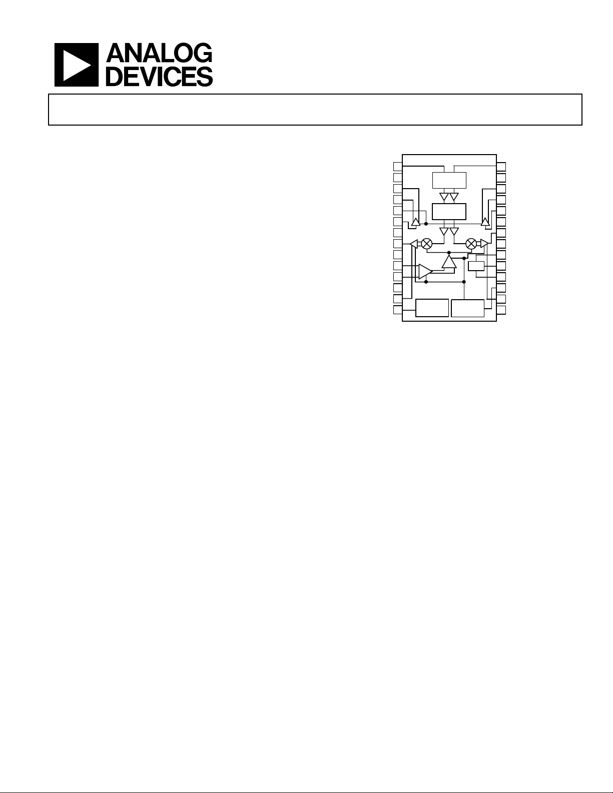
FEATURES FUNCTIONAL BLOCK DIAGRAM
Integrated RF and baseband AGC amplifiers
Quadrature phase accuracy 1° typ
I/Q amplitude balance 0.3 dB typ
Third-order intercept (IIP3) +11.5 dBm @ min gain
Noise figure 11 dB @ max gain
AGC range 69.5 dB
Baseband level control circuit
Low LO drive −8 dBm
ADC-compatible I/Q outputs
Single supply 2.7 V to 5.5 V
Power-down mode
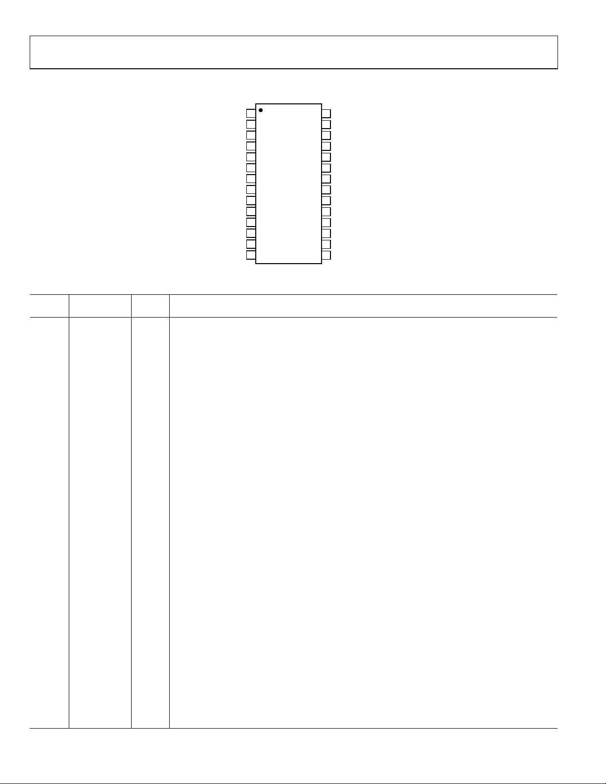
28-lead TSSOP package
APPLICATIONS
Cellular base stations
Radio links
Wireless local loop
IF broadband demodulators
RF instrumentation
Satellite modems
LOIN
VPS1
IOPN
IOPP
VCMO
IAIN
COM3
IMXO
COM2
RFIN
RFIP
VPS2
IOFS
VREF
1
2
3
4
5
6
7
8
9
10
11
12
13
14
AD8347
SPLITTER
SPLITTER
BIAS
PHASE
PHASE
CONTROL
Figure 1.
GAIN
DET
LOIP
28
COM1
27
26
QOPN
25
QOPP
24
QAIN
23
COM3
22
QMXO
21
VPS3
20
VDT1
19
VAGC
18
VDT2
17
GIN
V
16
QOFS
15
ENBL
02675-001
GENERAL DESCRIPTION
The AD83471 is a broadband direct quadrature demodulator
with RF and baseband automatic gain control (AGC) amplifiers.
It is suitable for use in many communications receivers, performing
quadrature demodulation directly to baseband frequencies. The
input frequency range is 800 MHz to 2.7 GHz. The outputs can
be connected directly to popular A-to-D converters such as the
AD9201 and AD9283.
The RF input signal goes through two stages of variable gain
amplifiers prior to two Gilbert-cell mixers. The LO quadrature
phase splitter employs polyphase filters to achieve high
quadrature accuracy and amplitude balance over the entire
operating frequency range. Separate I and Q channel variable
gain amplifiers follow the baseband outputs of the mixers. The
RF and baseband amplifiers together provide 69.5 dB of gain
control. A precision control circuit sets the linear-in-dB RF gain
response to the gain control voltage.
1
U.S. patents issued and pending.
Baseband level detectors are included for use in an AGC loop to
maintain the output level. The demodulator dc offsets are
minimized by an internal loop, whose time constant is
controlled by external capacitor values. The offset control can
also be overridden by forcing an external voltage at the offset
nulling pins.
The baseband variable gain amplifier outputs are brought offchip for filtering before final amplification. By inserting a
channel selection filter before each output amplifier, high level
out-of-channel interferers are eliminated. Additional internal
circuitry also allows the user to set the dc common-mode level
at the baseband outputs.
Rev. A
Information furnished by Analog Devices is believed to be accurate and reliable. However, no
responsibility is assumed by Anal og Devices for its use, nor for any infringements of patents or ot her
rights of third parties that may result from its use. Specifications subject to change without notice. No
license is granted by implication or otherwise under any patent or patent rights of Analog Devices.
Trademarks and registered trademarks are the property of their respective owners.
One Technology Way, P.O. Box 9106, Norwood, MA 02062-9106, U.S.A.
Tel: 781.329.4700 www.analog.com
Fax: 781.461.3113 © 2005 Analog Devices, Inc. All rights reserved.
Page 2

AD8347
TABLE OF CONTENTS
Features.............................................................................................. 1
LO and Phase Splitters............................................................... 16
Applications....................................................................................... 1
Functional Block Diagram .............................................................. 1
General Description ......................................................................... 1
Revision History ............................................................................... 2
Specifications..................................................................................... 3
Absolute Maximum Ratings............................................................ 5
ESD Caution.................................................................................. 5
Pin Configuration and Function Descriptions............................. 6
Typical Performance Characteristics ............................................. 8
RF Amp and Demodulator ......................................................... 8
Baseband Output Amplifiers ....................................................11
RF Amp/Demod and Baseband Output Amplifiers.............. 12
Equivalent Circuits..................................................................... 14
Theory of Operation ...................................................................... 16
RF Variable Gain Amplifiers (VGA)........................................ 16
Output Level Detector............................................................... 17
Bias ............................................................................................... 17
Applications..................................................................................... 18
Basic Connections...................................................................... 18
RF Input and Matching ............................................................. 18
LO Drive Interface ..................................................................... 18
Operating the VGA.................................................................... 19
Mixer Output Level and Drive Capability .............................. 19
Operating the VGA in AGC Mode .......................................... 19
Changing the AGC Setpoint..................................................... 20
Baseband Amplifiers.................................................................. 20
Driving Capacitive Loads.......................................................... 21
External Baseband Amplification ............................................ 21
Filter Design Considerations.................................................... 21
DC Offset Compensation.......................................................... 22
Mixers .......................................................................................... 16
Baseband Variable Gain Amplifiers......................................... 16
Output Amplifiers...................................................................... 16
REVISION HISTORY
10/05—Rev. 0 to Rev. A
Updated Format..................................................................Universal
Change V
Changes to Figure 46...................................................................... 19
Changes to Figure 48 ..................................................................... 21
Changes to Figure 49 and Figure 50............................................. 22
Changes to Ordering Guide.......................................................... 27
10/01—Revision 0: Initial Version
GIN
to V
..........................................................Universal
VGIN
Evaluation Board............................................................................ 23
Outline Dimensions....................................................................... 26
Ordering Guide .......................................................................... 26
Rev. A | Page 2 of 28
Page 3

AD8347
SPECIFICATIONS
VS = 5 V; TA = 25°C; FLO = 1.9 GHz; V
otherwise noted.
Table 1.
Parameter Conditions Min Typ Max Unit
OPERATING CONDITIONS
LO/RF Frequency Range 0.8 2.7 GHz
LO Input Level −10 0 dBm
VGIN Input Level 0.2 1.2 V
V
(VS) 2.7 5.5 V
SUPPLY
Temperature Range −40 +85 °C
RF AMPLIFIER/DEMODULATOR From RFIP/RFIN to IMXO and QMXO (IMXO/QMXO load > 1 kΩ)
AGC Gain Range 69.5 dB
Conversion Gain (Max) V
Conversion Gain (Min) V
Gain Linearity V
Gain Flatness FLO = 0.8 GHz to 2.7 GHz, FBB = 1 MHz +0.7 dB p-p
Input P1 dB V
V
Third-Order Input Intercept (IIP3) F
F
Second-Order Input Intercept (IIP2) F
F
LO Leakage (RF) At RFIP −60 dBm
LO Leakage (MXO) At IMXO/QMXO −42 dBm
Demodulation Bandwidth −3 dB +90 MHz
Quadrature Phase Error FRF = 1.9 GHz −3 ±1 +3 degree
I/Q Amplitude Imbalance FRF = 1.9 GHz +0.3 dB
Noise Figure Max Gain 11 dB
Mixer AGC Output Level See Figure 34 24 mV p-p
Baseband DC Offset At IMXO/QMXO, max gain (corrected, REF to VREF) 2 mV
Mixer Output Swing Level at which IMD3 = 45 dBc
R
R
Mixer Output Impedance 3 Ω
BASEBAND OUTPUT AMPLIFIER From IAIN to IOPP/IOPN and QAIN to QOPP/QOPN
Gain 30 dB
Bandwidth −3 dB (see Figure 22) 65 MHz
Output DC Offset (Differential) (V
Common-Mode Offset (V
Group Delay Flatness 0 MHz to 50 MHz +1.8 ns p-p
Second-Order Intermod. Distortion FIN1 = 5 MHz, FIN2 = 6 MHz, VIN1 = VIN2 = 8 mV p-p −49 dBc
Third-Order Intermod. Distortion FIN1 = 5 MHz, FIN2 = 6 MHz, VIN1 = VIN2 = 8 mV p-p −67 dBc
Input Bias Current +2 µA
Input Impedance 1||3 MΩ||pF
Output Swing Limit (Upper) VS − 1.3 V
Output Swing Limit (Lower) 0.4 V
= 1 V; FRF = 1.905 GHz; PLO = −8 dBm, R
VCMO
= 0.2 V (max gain) 39.5 dB
VGIN
= 1.2 V (min gain) −30 dB
VGIN
= 0.3 V to 1 V ±2 dB
VGIN
= 0.2 V −30 dBm
VGIN
= 1.2 V −2 dBm
VGIN
= 1.905 GHz, +11.5 dBm
RF1
= 1.906 GHz, –10 dBm each tone, (min gain)
RF2
= 1.905 GHz, +25.5 dBm
RF1
= 1.906 GHz, −10 dBm each tone, (min gain)
RF2
= 200 Ω 65 mV p-p
LOAD
= 1 kΩ 65 mV p-p
LOAD
= 10 kΩ, dBm with respect to 50 Ω, unless
LOAD
R
= 10 kΩ
LOAD
– V
IOPP
IOPP
) −200 ±50 +200 mV
IOPN
+ V
IOPN
)/2 − V
−40 ±5 +40 mV
VCMO
Rev. A | Page 3 of 28
Page 4

AD8347
Parameter Conditions Min Typ Max Unit
CONTROL INPUT/OUTPUTS
VCMO Input @ VS = 2.7 V 1 V
@ VS = 5 V 0.5 1 2.5 V
Gain Control Input Bias Current VGIN <1 µA
Offset Input Overriding Current IOFS, QOFS 10 µA
VREF Output R
RESPONSE FROM RF INPUT TO FINAL
BB AMP
Gain @ V
Gain @ V
= 0.2 V 65.5 69.5 72.5 dB
VGIN
= 1.2 V −3 +0.5 +4 dB
VGIN
Gain Slope −96.5 −89 −82.5 dB/V
Gain Intercept Linear extrapolation back to theoretical value at VGIN = 0 88 94 101 dB
LO/RF INPUT (See Figure 30 through Figure 33 for more detail)
LOIP Input Return Loss Measuring LOIP LOIN, ac-coupled to ground with 100 pF. −4 dB
Measuring through evaluation board balun with termination −9.5 dB
RFIP Input Return Loss RFIP input pin −10 dB
ENABLE
Power-Up Control Low = standby 0 0.5 V
Power-Up Control High = enabled +VS − 1 +VS V
Power-Up Time Time for final BB amps to be within 90% of final amplitude
@ VS = 5 V 20 µs
@ VS = 2.7 V 10 µs
Power-Down Time Time for supply current to be <4 mA
@ VS = 5 V 30 µs
@ VS = 2.7 V 1.5 ms
POWER SUPPLIES VPS1, VPS2, VPS3
Voltage 2.7 5.5 V
Current (Enabled) @ 5 V 48 64 80 mA
Current (Standby) @ 5 V 400 µA
Current (Standby) @ 3.3 V 80 µA
= 10 kΩ 0.95 1.00 1.05 V
LOAD
IMXO and QMXO connected directly to IAIN and QAIN,
respectively
Rev. A | Page 4 of 28
Page 5

AD8347
ABSOLUTE MAXIMUM RATINGS
Table 2.
Parameter Rating
Supply Voltage VPS1, VPS2, VPS3 5.5 V
LO and RF Input Power 10 dBm
Internal Power Dissipation 500 mW
θJA 68°C/W
Maximum Junction Temperature 150°C
Operating Temperature Range −40°C to +85°C
Storage Temperature Range −65°C to +150°C
Lead Temperature (Soldering 60 sec) 300°C
Stresses above those listed under Absolute Maximum Ratings
may cause permanent damage to the device. This is a stress
rating only; functional operation of the device at these or any
other conditions above those indicated in the operational
section of this specification is not implied. Exposure to absolute
maximum rating conditions for extended periods may affect
device reliability.
ESD CAUTION
ESD (electrostatic discharge) sensitive device. Electrostatic charges as high as 4000 V readily accumulate on
the human body and test equipment and can discharge without detection. Although this product features
proprietary ESD protection circuitry, permanent damage may occur on devices subjected to high energy
electrostatic discharges. Therefore, proper ESD precautions are recommended to avoid performance
degradation or loss of functionality.
Rev. A | Page 5 of 28
Page 6
AD8347
PIN CONFIGURATION AND FUNCTION DESCRIPTIONS
LOIN
VPS1
IOPN
IOPP
VCMO
IAIN
COM3
IMXO
COM2
RFIN
RFIP
VPS2
IOFS
VREF
1
2
3
4
5
6
7
8
9
10
11
12
13
14
AD8347
TOP VIEW
(Not to Scale)
LOIP
28
COM1
27
26
QOPN
25
QOPP
24
QAIN
23
COM3
22
QMXO
21
VPS3
20
VDT1
19
VAGC
18
VDT2
17
GIN
V
16
QOFS
15
ENBL
02675-002
Figure 2. 28-Lead TSSOP Pin Configuration
Table 3. Pin Function Descriptions
Equiv.
Pin No. Mnemonic Description
1, 28 LOIN, LOIP A
Circuit
LO Input. For optimum performance, these inputs are differentially driven. Typical input drive level is
equal to −8 dBm. To improve the match to a 50 Ω source, connect a 200 Ω shunt resistor between LOIP
and LOIN. A single-ended drive is possible, but slightly increases LO leakage.
2 VPS1 Positive Supply for LO Section. Decouple VPS1 with 0.1 µF and 100 pF capacitors.
3, 4 IOPN, IOPP B
I-Channel Differential Baseband Output. Typical output swing is equal to 760 mV p-p differential in
AGC mode. The common-mode level on these pins is programmed by the voltage on VCMO.
5 VCMO C
Baseband Amplifier Common-Mode Voltage. The voltage applied to this pin sets the output common-
mode level of the baseband amplifiers. This pin can either be connected to VREF (Pin 14) or to a
reference voltage from another device (typically an ADC).
6 IAIN D
I-Channel Baseband Amplifier Input. This pin, which has a high input impedance, should be biased to
VREF (approximately 1 V). If IAIN is connected directly to IMXO, biasing is provided by IMXO. If an ac-
coupled filter is placed between IMXO and IAIN, this pin can be biased from VREF through a 1 kΩ
resistor. The gain from IAIN to the differential outputs IOPN/IOPP is 30 dB.
7, 23 COM3 Ground for Biasing and Baseband Sections.
8, 22 IMXO, QMXO B
I-Channel and Q-Channel Baseband Mixer/VGA Outputs. Low impedance outputs with bias levels equal to
VREF. IMXO and QMXO are typically connected to IAIN and QAIN, respectively, either directly or through
filters. These outputs have a maximum current limit of about 1.5 mA. This allows for a 600 mV p-p swing into
a 200 Ω load. This corresponds to an input level of −40 dBm @ a maximum gain of 39.5 dB. At lower output
levels, IMXO and QMXO can drive a lower load resistance, subject to the same current limit.
9 COM2 RF Section Ground.
10, 11 RFIN, RFIP E
RF Input. RFIN must be ac-coupled to ground. The RF input signal should be ac-coupled into RFIP. For
a broadband 50 Ω input impedance, connect a 200 Ω resistor from the signal side of the RFIP coupling
capacitor to ground. Note that RFIN and RFIP are not interchangeable differential inputs. RFIN is the
ground reference for the input system.
12 VPS2 Positive Supply for RF Section. Decouple VPS2 with 0.1 µF and 100 pF capacitors.
13, 16 IOFS, QOFS F
I-Channel and Q-Channel Offset Nulling Inputs. To null the dc offset on the I-channel and Q-channel
mixer outputs (IMXO, QMXO), connect a 0.1 µF capacitor from these pins to ground. Alternately, a
forced voltage of approximately 1 V on these pins disables the offset compensation circuit.
14 VREF G
Reference Voltage Output. This output voltage (1 V) is the main bias level for the device and can be
used to externally bias the inputs and outputs of the baseband amplifiers. The VREF pin should be
decoupled with a 0.1 F capacitor to ground.
15 ENBL H Chip Enable Input. Active high.
17 VGIN C
Gain Control Input. The voltage on this pin controls the gain on the RF and baseband VGAs. The gain
control is applied in parallel to all VGAs. The gain control voltage range is from 0.2 V to 1.2 V and
corresponds to a gain range from +39.5 dB to −30 dB. This is the gain to the output of the baseband
VGAs (that is, QMXO and IMXO). There is an additional 30 dB of gain in the baseband amplifiers. Note
that the gain control function has a negative sense (that is, increasing control voltage decreases gain).
In AGC mode, connect this pin directly to VAGC.
Rev. A | Page 6 of 28
Page 7
AD8347
Equiv.
Pin No. Mnemonic Description
18, 20 VDT2, VDT1 D
19 VAGC I
21 VPS3 Positive Supply for Biasing and Baseband Sections. Decouple VPS3 with 0.1 µF and 100 pF capacitors.
24 QAIN D
25, 26 QOPP, QOPN B
27 COM1 LO Section Ground.
Circuit
ENBL
RFIN
RFIP
Detector Inputs. These pins are the inputs to the on-board detector. VDT2 and VDT1, which have high
input impedances, are normally connected to IMXO and QMXO, respectively.
AGC Output. This pin provides the output voltage from the on-board detector. In AGC mode, connect
this pin directly to VGIN.
Q-Channel Baseband Amplifier Input. Bias this high input impedance pin to VREF (approximately 1 V).
If QAIN is directly connected to QMXO, biasing is provided by QMXO. If an ac-coupled filter is placed
between QMXO and QAIN, this pin can be biased from VREF through a 1 kΩ resistor. The gain from
QAIN to the QOPN/QOPP differential outputs is 30 dB.
Q-Channel Differential Baseband Output. Typical output swing is equal to 760 mV p-p differential. The
common-mode level on these pins is programmed by the voltage on VCMO.
VPS3
VPS2 IMXO
VPS1
12
2
AD8347
15
10
11
BIAS
CELL
VREF
21
VREF
814
VREF
PHASE
SPLITTER
IAIN
2
613
VCMO
IOPPIOFS IOPN
3
4
PHASE
SPLITTER
1
VCMO
5
LOIN
1
28
LOIP
VGIN
17
GAIN
CONTROL
INTERFACE
DET 1
20 19
DET 2
18
VDT2 QMXO QOPPQOFSVAGCVDT1 QAIN
22 16 24 25
VREF
Figure 3. Block Diagram
VCMO
26
QOPN
7
COM3
9
COM2
23
COM3
27
COM1
02675-003
Rev. A | Page 7 of 28
Page 8
AD8347
TYPICAL PERFORMANCE CHARACTERISTICS
RF AMP AND DEMODULATOR
,
,
2400 2600
14
12
10
8
6
4
2
0
–2
–4
–6
–8
–10
–12
14
12
10
8
6
4
2
0
–2
–4
–6
–8
–10
LINEARITY ERROR (dB)
02675-013
LINEARITY ERROR (dB)
02675-014
02675-015
MIXER GAIN (dB)
45
40
35
30
25
20
15
10
–5
–10
–15
–20
–25
–30
–35
TA = –40°C
TA = +85°C
TA = +25°C
5
0
TA = +25°C
TA = +85°C
0.3 0.4 0.5 0.6 0.7 0.8 0.9 1.0 1.1 1.2
0.2
V
VGIN
(V)
Figure 4. Gain and Linearity Error vs. V
= 5 V, FLO = 1900 MHz, FBB = 1 MHz
V
S
45
MIXER GAIN (dB)
–10
–15
–20
–25
–30
–35
40
35
30
25
20
15
10
5
0
–5
0.2
TA = –40°C
TA = +85°C
TA = –40°C
TA = +25°C
TA = +85°C
0.3 0.4 0.5 0.6 0.7 0.8 0.9 1.0 1.1 1.2
TA = +25°C
V
VGIN
(V)
Figure 5. Gain and Linearity Error vs. V
= 2.7 V, FLO = 1900 MHz, FBB = 1 MHz
V
S
40
39
VS = 2.7V, TA = –40°C
38
37
36
V
= 2.7V, TA = +85°C
S
35
GAIN (dB)
34
33
32
31
30
1000 1200 1400 1600 1800 2000 2200
800
Figure 6. Gain vs. F
VS = 2.7V, TA = +25°C
V
S
VS = 5V, TA = +85°C
RF FREQUENCY (MHz)
, V
= 0.2 V, FBB = 1 MHz
LO
VGIN
= 5V, TA = –40°C
TA = –40°C
VGIN
VGIN
= 5V, TA = +25°C
V
S
3.0
2.5
2.0
1.5
V
= 2.7V, TA = –40°C
S
1.0
GAIN (dB)
0.5
= 5V, TA = –40°C
V
S
0
–0.5
–1.0
800
1000 1200 1400 1600 1800 2000 2200
Figure 7. Gain vs. F
–27
–28
= 2.7V, TA = +25°C
V
S
–29
–30
–31
–32
GAIN (dB)
–33
V
= 5V, TA = +85°C
S
–34
–35
–36
–
37
800
1000 1200 1400 1600 1800 2000 2200
Figure 8. Gain vs. F
42
41
40
39
38
V
= 5V, TA = +25°C
S
37
36
V
= 2.7V, TA = +85°C
S
35
GAIN (dB)
34
= 5V, TA = +85°C
V
S
33
32
31
30
1
Figure 9. Gain vs. F
VS = 2.7V, TA = +25°C
V
RF FREQUENCY (MHz)
LO
= 5V, TA = +25°C
V
S
V
= 5V, TA = –40°C
S
RF FREQUENCY (MHz)
LO
= 2.7V, TA = –40°C
V
S
BASEBAND FREQUENCY (MHz)
, V
BB
= 5V, TA = +25°C
S
VS = 5V, TA = +85°C
VS = 2.7V, TA = +85°C
, V
= 0.7 V, FBB = 1 MHz
VGIN
= 2.7V, TA = –40°C
V
S
VS = 2.7V, TA = +85°C
, V
= 1.2 V, F
VGIN
10
= 0.2 V, FLO = 1900 MHz
VGIN
BB
VS = 2.7V, TA = +25°C
= 5V, TA = –40°C
V
S
2400 2600
2400 2600
= 1 MHz
100
02675-016
02675-017
02675-018
Rev. A | Page 8 of 28
Page 9
AD8347
10
9
8
7
6
5
4
= 2.7V, TA = +25°C
V
S
3
2
GAIN (dB)
1
0
–1
–2
= 5V, TA = –40°C
V
–3
S
–4
–5
1
Figure 10. Gain vs. FBB, V
VS = 2.7V, TA = +85°C
V
= 5V, TA = +85°C
S
= 5V, TA = +25°C
V
S
= 2.7V, TA = –40°C
V
S
BASEBAND FREQUENCY (MHz)
10
= 0.7 V, FLO = 1900 MHz
VGIN
100
02675-019
15
VS = 2.7V, TA = +85°C
14
13
12
11
10
V
= 2.7V, TA = +25°C
S
IIP3 (dBm)
9
8
7
6
5
800 2400 26001000 1200 1400 1600 1800 2000 2200
Figure 13. IIP3 vs. F
V
= 5V, TA = +85°C
S
= 5V, TA = +25°C
V
S
V
= 2.7V, TA = –40°C
S
V
= 5V, TA = –40°C
S
RF FREQUENCY (MHz)
, V
= 1.2 V, F
LO
VGIN
= 1 MHz
BB
02675-022
–25
–26
–27
–28
= 5V, TA = +25°C
V
S
–29
–30
GAIN (dB)
–31
–32
VS = 2.7V, TA = +85°C
–33
–34
–35
1
Figure 11. Gain vs. F
0
–5
–10
VS = 5V, TA = +85°C
–15
–20
INPUT P1dB (dBm)
–25
–30
V
–35
0.2
= 2.7V, TA = +25°C
V
S
BASEBAND FREQUENCY (MHz)
, V
BB
= 5V, TA = –40°C
V
S
VS = 2.7V, TA = +85°C
= 2.7V, TA = +25°C
V
S
= 2.7V, TA = –40°C
V
S
= 5V, TA = +25°C
S
V
VGIN
V
= 2.7V, TA = –40°C
S
V
= 5V, TA = –40°C
S
= 5V, TA = +85°C
V
S
10
= 1.2 V, FLO = 1900 MHz
VGIN
(V)
Figure 12. Input 1 dB Compression Point (OP1 dB) vs. V
= 1900 MHz, F
F
LO
= 1 MHz
BB
–10
–12
= 5V, TA = +25°C
V
S
–14
–16
–18
–20
IIP3 (dBm)
–22
–24
V
= 5V, TA = –40°C
S
–26
–28
100
02675-020
–30
800 2400 26001000 1200 1400 1600 1800 2000 2200
Figure 14. IIP3 vs. F
15
V
= 2.7V, TA = –40°C
S
14
V
13
IIP3 (dBm)
12
11
V
= 2.7V, TA = +25°C
S
10
0 100510
1.2
1.11.00.90.80.70.60.50.40.3
02675-021
,
VGIN
15 20 25 30 35 40 45 50 55 60 65 70 75 80 85 90 95
Figure 15. IIP3 vs. F
VS = 2.7V, TA = +85°C
= 2.7V, TA = +25°C
V
S
V
= 2.7V, TA = –40°C
S
= 5V, TA = +85°C
V
S
RF FREQUENCY (MHz)
, V
= 0.2 V, FBB = 1 MHz
LO
VGIN
= 5V, TA = +85°C
S
= 5V, TA = –40°C
V
S
BASEBAND FREQUENCY (MHz)
BB
VS = 2.7V, TA = +85°C
= 5V, TA = +25°C
V
S
, V
= 1.2 V, FLO = 1900 MHz
VGIN
02675-023
02675-024
Rev. A | Page 9 of 28
Page 10

AD8347
–10
–12
–14
V
= 5V, TA = +85°C
–16
–18
–20
–22
–24
IIP3 (dBm)
–26
–28
–30
–32
–34
IIP2 (dBm)
Figure 17. IIP2 vs. F
Baseband Tone2 = 6 MHz, −10 dBm, Temperature = 25°C, V
NOISE FIGURE (dB)
Figure 18. Noise Figure vs. LO Frequency (F
S
VS = 2.7V, TA = +85°C
= 5V, TA = +25°C
V
S
V
= 5V, TA = –40°C
S
V
= 2.7V, TA = +25°C
S
= 2.7V,
V
S
= –40°C
T
A
0 100510
15 20 25 30 35 40 45 50 55 60 65 70 75 80 85 90 95
BASEBAND FREQUENCY (MHz)
Figure 16. IIP3 vs. F
50
45
40
35
30
25
20
800
1000 1200 1400 1600 1800 2000 2200 2400 2600
13.0
12.5
12.0
11.5
11.0
10.5
10.0
800
1000 1200 1400 1600 1800 2000 2200 2400 2600
RF FREQUENCY (MHz)
= 1.2 V, Baseband Tone1 = 5 MHz, −10 dBm,
LO, VVGIN
VS = 5V
V
VGIN
= 0.2 V, FLO = 1900 MHz
BB, VVGIN
VS = 2.7V
LO FREQUENCY (MHz)
LO
= 0.2 V, FBB = 1 MHz
), Temperature = 25°C,
= 5 V
S
02675-025
02675-026
02675-027
70
60
50
40
30
NOISE FIGURE (dB)
20
10
VS = 2.7V
VS = 5V
0
0.2
0.3 0.4 0.5 0.6 0.7 0.8 0.9 1.0
VS = 5V
VS = 2.7V
V
VGIN
Figure 19. Noise Figure and IIP3 vs. V
= 1900 MHz, FBB = 1 MHz
F
LO
2.5
2.0
1.5
1.0
0.5
0
–0.5
–1.0
LO FREQUENCY = 800MHz
–1.5
–2.0
QUADRATURE PHASE ERROR (Degrees)
–2.5
–20
–18 –16 –14 –12 –10 –8 –6 –4
LO FREQUENCY = 1900MHz
LO INPUT LEVEL (dBm)
(V)
, Temperature = 25°C,
VGIN
LO FREQUENCY = 2700MHz
15
10
5
0
–5
–10
–15
–20
–25
–30
–2
0
Figure 20. Quadrature Error vs. LO Power Level, Temperature = 25°C,
V
= 0.2 V, VS = 5 V
VGIN
14.0
13.5
13.0
12.5
12.0
11.5
11.0
NOISE FIGURE (dB)
10.5
10.0
9.5
9.0
–20
–18 –16 –14 –12 –10 –8 –6 –4
2700MHz
1900MHz
800MHz
LO INPUT LEVEL (dBm)
0
–2
Figure 21. Noise Figure vs. LO Input Level, Temperature = 25°C,
V
= 0.2 V, VS = 5 V
VGIN
IIP3
02675-028
02675-029
02675-030
Rev. A | Page 10 of 28
Page 11

AD8347
BASEBAND OUTPUT AMPLIFIERS
34
= –40°C, VS = 5V
T
A
32
30
28
26
24
GAIN (dB)
22
20
18
16
1 10010
T
= +25°C, VS = 5V
A
= +85°C, VS = 2.7V
T
A
BASEBAND FREQUENCY (MHz)
Figure 22. Gain vs. F
T
= –40°C, VS = 2.7V
A
TA = +25°C, VS = 2.7V
TA = +85°C, VS = 5V
, V
= 1 V
BB
VCMO
02675-031
20
15
10
5
0
–5
–10
–15
–20
–25
BASEBAND AMPLIFIER OUTPUT IP3 (dBV rms)
–30
1
= –40°C, VS = 5V
T
A
= +25°C, VS = 2.7V
T
A
= +85°C, VS = 2.7V
T
A
Figure 24. OIP3 vs. F
T
= +25°C, VS = 5V
A
TA = +85°C, VS = 5V
= –40°C, VS = 2.7V
T
A
BASEBAND FREQUENCY (MHz)
10
, V
= 1 V
BB
VCMO
100
02675-033
5
TA = –40°C, VS = 5V
0
–5
TA = +25°C, VS = 2.7V
–10
TA = +85°C, VS = 2.7V
OP1 (dBV rms)
–15
–20
–25
1 10010
TA = +25°C, VS = 5V
TA = –40°C, VS = 2.7V
BASEBAND FREQUENCY (MHz)
Figure 23. OP1 vs. F
TA = +85°C, VS = 5V
, V
= 1 V
BB
VCMO
02675-032
8
VS = 2.7V, MEAN +
6
4
2
0
–2
VS = 2.7V, MEAN–
COMMON-MODE OFFSET (mV)
–4
–6
0.5 3.52.0
1.0 1.5 2.5 3.0
σ
VS = 2.7V, MEAN
VS = 5V, MEAN
σ
V
VCMO
VS = 5V, MEAN +
VS = 5V, MEAN–
(V)
Figure 25. Common-Mode Output Offset Voltage vs. V
Temperature = 25°C (σ = 1 Standard Deviation)
σ
σ
02675-034
,
VCMO
Rev. A | Page 11 of 28
Page 12

AD8347
RF AMP/DEMOD AND BASEBAND OUTPUT AMPLIFIERS
75
= –40°C, VS = 2.7V
T
65
55
TA = +85°C,
VS = 2.7V
45
35
TA = +85°C, VS = 5V
25
VOLTAGE GAIN (dB)
15
5
–5
0.2 0.80.5
0.3 0.4 0.6 0.7
Figure 26. Voltage Gain vs. V
A
TA = –40°C, VS = 5V
T
= +25°C, VS = 2.7V
A
TA = +25°C, VS = 5V
V
(V)
VGIN
, FLO = 1900 MHz, FBB = 1 MHz
VGIN
0.9 1.0 1.1 1.2
02675-035
1.0
0.8
0.6
0.4
0.2
TA = +85°C
T
0
–0.2
–0.4
–0.6
I TO Q AMPLITUDE MISMATCH (dB)
–0.8
–1.0
0 5 10 15 20 25 30 35 40
= +25°C
A
= –40°C
T
A
BASEBAND FREQUENCY (MHz)
02675-038
Figure 29. I/Q Amplitude Imbalance vs. FBB, Temperature = 25°C, VS = 5 V
2.5
2.0
1.5
1.0
0.5
0
–0.5
–1.0
–1.5
QUADRATURE PHASE ERROR (Degrees)
–2.0
–2.5
800
= +25°C, VS = 5V
T
A
TA = +85°C, VS = 5V
1000 1200 1400 1600 1800 2000 2200
RF FREQUENCY (MHz)
Figure 27. Quadrature Phase Error vs. F
2.5
2.0
1.5
1.0
0.5
0
–0.5
–1.0
–1.5
QUADRATURE PHASE ERROR (Degrees)
–2.0
–2.5
0
5 101520253035
TA = +85°C
= –40°C
T
A
BASEBAND FREQUENCY (MHz)
Figure 28. Quadrature Phase Error vs. F
T
= +25°C
A
= –40°C, VS = 5V
T
A
, V
= 0.7 V, VS = 5 V
LO
VGIN
, V
= 0.7 V, VS = 5 V
BB
VGIN
2400 2600
40
02675-036
02675-037
0
–
2
–
4
–
6
RF WITH TERMINATION
8
–
RETURN LOSS (dBm)
–10
RF WITHOUT TERMINATION
–12
800
1000 1200 1400 1600 1800 2000 2200
Figure 30. Return Loss of RFIP vs. F
2.7GHz
RF FREQUENCY (MHz)
2.7GHz
, V
RF
VGIN
WITH TERMINATION
800MHz
800MHz
WITHOUT TERMINATION
, V
Figure 31. S11 of RFIN vs. F
RF
VGIN
= 0.7 V, VS = 5 V
2400 2600
= 0.7 V, VS = 5 V
02675-040
02675-039
Rev. A | Page 12 of 28
Page 13

AD8347
0
–2
–4
–6
–8
RETURN LOSS (dBm)
–10
–12
–14
800
LO PORT WITHOUT TERMINATION
LO PORT WITH TERMINATION
1000 1200 1400 1600 1800 2000 2200
RF FREQUENCY (MHz)
Figure 32. Return Loss of LOIP vs. F
, V
LO
VGIN
2400 2600
= 0.7 V, VP = 5 V
02675-041
30
T
= +85°C
A
25
20
T
A
15
10
5
MIXER OUTPUT VOLTAGE (mV p-p)
0
–70
T
= +25°C
–60 –50 –40 –30 –20 –10 0 10
TA = –40°C
= +85°C
A
RF INPUT POWER (dBm)
= +25°C
T
A
TA = –40°C
1.20
1.00
0.80
0.60
0.40
0.20
0
Figure 34. AGC Voltage and Mixer Output Level vs. RF Input Power,
= 1900 MHz, FBB = 1 MHz, V
F
LO
85
= 5 V
S
AGC VOLTAGE (V)
02675-043
WITH TERMINATION
800MHz
2.7GHz
2.7GHz
WITHOUT TERMINATION
Figure 33. S11 of LOIN vs. F
800MHz
, V
LO
VGIN
= 0.7 V, VS = 5 V
02675-042
80
75
70
65
60
SUPPLY CURRENT (mA)
55
50
45
–40
VP = 5.5V
VP = 2.7V
–30 –20 –10
VP = 5V
VP = 3V
0 102030
TEMPERATURE (°C)
Figure 35. Supply Current vs. Temperature, V
40 50
VGIN
60 70 80
= 0.7 V, V
VCMO
= 1 V
02675-044
Rev. A | Page 13 of 28
Page 14

AD8347
EQUIVALENT CIRCUITS
VPS1
VPS3
LOIN
LOIP
COM1
Figure 36. Circuit A
COM3
Figure 37. Circuit B
CONTINUES
VPS3
IOPP, IOPN,
QOPP, QOPN,
IMXO, QMXO
PHASE
SPLITTER
02675-005
02675-004
RFIP
RFIN
VPS2
IAIN
QAIN
Figure 39. Circuit D
COM2
Figure 40. Circuit E
COM3
02675-007
02675-008
VCMO
VPS3
CURRENT MIRROR
COM3
Figure 38. Circuit C
02675-006
IOFS
QOFS
VPS3
CURRENT MIRROR
COM3
Figure 41. Circuit F
02675-009
Rev. A | Page 14 of 28
Page 15

AD8347
VPS3
VPS3
COM3
Figure 42. Circuit G
VPS3
ENBL
COM3
VREF
02675-010
02675-011
COM3
Figure 44. Circuit I
VAGC
02675-012
Figure 43. Circuit H
Rev. A | Page 15 of 28
Page 16

AD8347
THEORY OF OPERATION
VPS1
AD8347
VPS3
VPS2 IMXO
VREF
VREF
IAIN
IOPPIOFS IOPN
461381421122
3
ENBL
RFIN
RFIP
VGIN
15
10
11
17
BIAS
CELL
GAIN
CONTROL
INTERFACE
VREF
DET 1
20 19 18 22 16 24 25
DET 2
VDT2 QMXO QOPPQOFSVAGCVDT1 QAIN
Figure 45. Block Diagram
The AD8347 is a direct I/Q demodulator usable in digital
wireless communication systems including cellular, PCS, and
digital video receivers. An RF signal in the frequency range of
800 MHz to 2,700 MHz is directly downconverted to the I and
Q components at baseband using a local oscillator (LO) signal
at the same frequency as the RF signal.
The RF input signal goes through two stages of variable gain
amplifiers before splitting up to reach two Gilbert-cell mixers.
The mixers are driven by a pair of LO signals which are in
quadrature (90 degrees of phase difference). The outputs of the
mixers are applied to baseband I-channel and Q-channel
variable gain amplifiers. The outputs from these baseband
variable gain amplifiers are brought out to pins for external
filtering. The filter outputs are then applied to a pair of on-chip,
fixed gain, baseband amplifiers. These amplifiers gain up the
outputs from the external filters to a level compatible with most
A-to-D converters. A sum of squares detector is available for
use in an automatic gain control (AGC) loop to set the output
level. The RF and baseband amplifiers provide approximately
69.5 dB of gain control range. Additional on-chip circuits allow
the setting of the dc level at the I-channel and Q-channel
baseband outputs, as well as nulling the dc offset at each
channel.
RF VARIABLE GAIN AMPLIFIERS (VGA)
These amplifiers use the patented X-AMP® approach with NPN
differential pairs separated by sections of resistive attenuators.
The gain control is achieved through a gaussian interpolator
where the control voltage sets the tail currents supplied to the
various differential pairs according to the gain desired. In the
first amplifier, the combined output currents from the
transconductance cells go through a cascode stage to resistive
loads with inductive peaking. In the second amplifier, the
Rev. A | Page 16 of 28
VCMO
5
LOIN
1
1
28
LOIP
7
COM3
9
COM2
23
COM3
27
26
COM1
02675-045
PHASE
SPLITTER
VREF
2
VCMO
PHASE
SPLITTER
VCMO
QOPN
differential currents are split and fed to the two Gilbert-cell
mixers through separate cascode stages.
MIXERS
Two double balanced Gilbert-cell mixers, one for each channel,
perform the in-phase (I) and quadrature (Q) down conversion.
Each mixer has four cross-connected transistor pairs that are
terminated in resistive loads and feed the differential baseband
variable gain amplifiers for each channel. The quadrature LO
signals drive the bases of the mixer transistors.
BASEBAND VARIABLE GAIN AMPLIFIERS
The baseband VGAs also use the X-AMP approach with NPN
differential pairs separated by sections of resistive attenuators.
The same interpolator controlling the RF amplifiers controls the
tail currents of the differential pairs. The outputs of these amplifiers
are provided off chip for external filtering. Automatic offset
nulling minimizes the dc offsets at both I- and Q-channels. The
common-mode output voltage is set to the same level as the
reference voltage (1.0 V) generated in the Bias cell, also made
available at the VREF pin (see
Figure 45).
OUTPUT AMPLIFIERS
The output amplifiers gain up the signal coming back from each of
the external filters to a level compatible with most high speed A-toD converters. These amplifiers are based on an active feedback
design to achieve high gain bandwidth with low distortion.
LO AND PHASE SPLITTERS
The incoming LO signal is applied to a polyphase phase splitter
to generate the LO signals for the I-channel and Q-channel
mixers. The polyphase phase splitters are RC networks
connected in a cyclical manner to achieve gain balance and
phase quadrature. The wide operating frequency range of these
phase splitters is achieved by cascading multiple sections of
Page 17

AD8347
these networks with staggered RC constants. Each branch goes
through a buffer to make up for the loss and high frequency
roll-off. The output from the buffers then goes into another
polyphase phase splitter to enhance the accuracy of phase
quadrature. Each LO signal is buffered again to drive the
mixers.
OUTPUT LEVEL DETECTOR
To create an AGC voltage (VAGC), two signals proportional to
the square of each output channel are summed together and
compared to a built-in threshold. The inputs to this rms
detector are referenced to VREF.
BIAS
An accurate reference circuit generates the reference currents
used by the different sections. The reference circuit is controlled
by an external power-up (ENBL) logic signal that, when set low,
puts the whole chip into a sleep mode typically requiring less
than 400 µA of supply current. The reference voltage (VREF) of
1.0 V, that serves as the common-mode reference for the
baseband circuits, is made available for external use. The VREF
pin should be decoupled with a 0.1 F capacitor to ground.
Rev. A | Page 17 of 28
Page 18

AD8347
APPLICATIONS
BASIC CONNECTIONS RF INPUT AND MATCHING
The basic connections for operating the AD8347 are shown in The RF input signal should be ac-coupled into the RFIP pin and
Figure 46. The device is powered through three power supply
pins: VPS1, VPS2, and VPS3. These pins supply current to
different parts of the overall circuit. VPS1 and VPS2 power the
local oscillator (LO) and RF sections, respectively, while VPS3
powers the baseband amplifiers. Connect all of these pins to the
same supply voltage; however, separately decouple each pin
using two capacitors. 100 pF and 0.1 µF capacitors are
recommended, though values close to these can be used.
Use a supply voltage in the range 2.7 V to 5.5 V. The quiescent
current is 64 mA when operating from a 5 V supply. By pulling
the ENBL pin low, the device goes into its power-down mode.
The power-down current is 400 µA when operating on a 5 V
supply and 80 µA on a 2.7 V supply.
Like the supply pins, the individual sections of the circuit are
separately grounded. COM1, COM2, and COM3 provide
ground for the LO, RF, and baseband sections, respectively.
Connect all of these pins to the same low impedance ground.
RFIN should be ac-coupled to ground. To improve broadband
matching to a 50 Ω source, a 200 Ω resistor can be connected
from the signal side of the RFIP coupling capacitor to ground.
LO DRIVE INTERFACE
For optimum performance, the LO inputs, LOIN and LOIP,
should be driven differentially; the M/A-COM balun, ETC1-1-13
is recommended. Unless an ac-coupled transformer is used to
generate the differential LO, the inputs must be ac-coupled, as
shown in
source, connect a 200 Ω shunt resistor between LOIP and LOIN.
A LO drive level of −8 dBm is recommended.
the relationship between LO drive level, LO frequency, and
quadrature error for a typical device.
A single-ended drive is also possible as shown in
this slightly increases LO leakage. Apply the LO signal through
a coupling capacitor to LOIP, and ac-couple LOIN to ground.
Because the inputs are fully differential, the drive orientation
can be reversed. As in the case of the differential drive, a 200 Ω
resistor connected across LOIP and LOIN improves the match
to a 50 Ω source.
Figure 46. To improve broadband matching to a 50 Ω
Figure 20 shows
Figure 47
, but
RF INPUT
0.8GHz–2.7GHz
0dBm MAX
(AGC MODE)
100pF
R1
200Ω
100pF
+V
S
(2.7V–5.5V)
C9
C6
0.1μF
C5
100pF
VPS1
2
C7
0.1μF
C8
100pF
VPS2
AD8347
15
C1
ENBL
RFIN
10
RFIP
VGIN
11
17
GAIN
CONTROL
INTERFACE
C2
C10
0.1μF
100pF
VPS3
VREF
2112
BIAS
CELL
DET 1
20 19 18 22 16
VDT2
C16
0.1μF
IMXO
VREF
DET 2
QMXO QOPP
C15
0.1μF
24mV p-p
(AGC MODE)
1V BIAS (VREF)
814
24mV p-p
(AGC MODE)
1V BIAS (VREF)
C13
0.1μF
IOFS
IAIN
613
VREF
VCMO
PHASE
SPLITTER
2
VREF
24 25
QOFSVAGCVDT1 QAIN
C14
0.1μF
IOPP
4
SPLITTER
VCMO
3
PHASE
1
26
IOPN
QOPN
5
1
28
7
9
23
27
VCMO
LOIN
LOIP
COM3
COM2
COM3
COM1
C4
100pF
R17
200Ω
C3
100pF
ETC 1-1-13
(M/A-COM)
IOPP
760mV p-p
DIFFERENTIAL
(AGC MODE)
V
= 1V
CM
IOPN
LO INPUT
–8dBm
0.8GHz–2.7GHz
3
4
15
T1
QOPN
760mV p-p
DIFFERENTIAL
(AGC MODE)
V
= 1V
CM
Figure 46. Basic Connections
Rev. A | Page 18 of 28
QOPP
02675-046
Page 19

AD8347
100pF
LO
200
100pF
Figure 47. Single-Ended LO Drive
LOIN
Ω
AD8347
LOIP
02675-047
OPERATING THE VGA
A three-stage VGA sets the gain in the RF section. Two of the
three stages come before the mixer while the third amplifies the
mixer output. All three stages are driven in parallel. The gain
range of the first RF VGA and that of the second RF VGA
combined with the mixer are both −13 dB to +10 dB. The gain
range of the baseband VGA is −4 dB to +19.5 dB. Therefore, the
overall gain range from the RF input to the IMXO and QMXO
pins is −30 dB to approximately +39.5 dB.
The gain of the VGA is set by the voltage on the VGIN pin,
which is a high impedance input. The gain control function
(which is linear-in-dB) and linearity are shown in
Figure 4 and
Figure 5 at 1.9 GHz. Note that the sense of the gain control
voltage is negative because as the gain control voltage ranges
from 0.2 V to 1.2 V, the gain decreases from +39.5 dB to −30 dB.
MIXER OUTPUT LEVEL AND DRIVE CAPABILITY
I- and Q-channel baseband outputs, IMXO and QMXO, are
low impedance outputs (R
V
, the voltage on Pin 14. The achievable output levels on
VREF
IMXO/QMXO are limited by their current drive capability of
1.5 mA maximum. This allows for a 600 mV p-p swing into a
200 Ω load. At lower output levels, IMXO and QMXO can drive
smaller load resistances, subject to the same current limit.
@ 3 Ω) with bias levels equal to
OUT
These output stages are not, however, designed to directly drive
50 Ω loads.
OPERATING THE VGA IN AGC MODE
Although the VGA can be driven by an external source such as
a DAC, the AD8347 has an on-board sum of squares detector to
allow the AD8347 to operate in an automatic leveling mode.
Due to the nature of the detector, an input signal with a higher
peak-to-average ratio causes the AGC loop to settle with a
higher mixer output peak-to-peak voltage. In this data sheet,
peak-to-peak calculations assume a sine wave input when
referencing AGC operation.
The connections for operating in this mode are shown in
Figure 46. The two mixer outputs are connected to Detector
Input VDT1 and Detector Input VDT2. The summed detector
output drives an internal integrator which, in turn, delivers a
gain correction voltage to the VAGC pin. A 0.1 µF capacitor
from VAGC to ground sets the dominant pole of the integrator
circuit. VAGC, which should be connected to VGIN, adjusts
gain until an internal threshold is reached. This threshold
corresponds to a level at the IMXO and QMXO pins of approximately 8.5 mV rms. This level changes slightly as a function of
RF input power (see
this corresponds to approximately 24 mV p-p. If this signal is
applied directly to the subsequent baseband amplifier stage,
the final baseband output is 760 mV p-p differential. See the
Baseband Amplifiers section.
If the VGA gain is set from an external source, VDT1 and
VDT2 (the on-board detector inputs) are not used and are tied
to VREF.
Figure 34). For a CW (sine wave) input,
Rev. A | Page 19 of 28
Page 20

AD8347
C1
100pF
R1
200
C2
100pF
RF
INPUT
R19
1k
IMXO
R21
4kΩ
R22
1kΩ
R20
4k
814
Ω
Ω
120mV p-p
1V BIAS
120mV p-p
C13
0.1
μ
F
IOFS
IAIN
VREF
PHASE
SPLITTER
2
VREF
QOFSVAGCVDT1 QAIN
C14
0.1
μ
F
1V BIAS
613
VCMO
IOPP
4
SPLITTER
VCMO
3
PHASE
1
26
IOPN
QOPN
5
1
28
7
9
23
27
VCMO
LOIN
LOIP
COM3
COM2
COM3
COM1
2.5V
C4
100pF
R17
200
C3
100pF
3
Ω
15
ETC 1-1-13
(M/A-COM)
IOPP
3.8V p-p
DIFFERENTIAL
V
= 2.5V
CM
IOPN
LO INPUT
–8dBm
0.8GHz–2.7GHz
4
T1
QOPN
3.8V p-p
DIFFERENTIAL
= 2.5V
V
CM
QOPP
02675-048
+VS +5V
C9
C6
0.1μF
C5
100pF
VPS1
C8
C7
100pF
0.1
μ
F
VPS2
2
AD8347
15
ENBL
RFIN
Ω
RFIP
VGIN
10
11
17
CELL
GAIN
CONTROL
INTERFACE
C10
0.1
μ
F
100pF
VPS3
12
BIAS
21
DET 1
20 19 18 22 16 24 25
VREF
VDT2
C16
0.1μF
VREF
DET 2
QMXO QOPP
Figure 48. Adjusting AGC Level to Increase Baseband Amplifier Output Swing
CHANGING THE AGC SETPOINT
The AGC circuit can be easily set up to level at voltages higher
than the nominal 24 mV p-p, as shown in
Figure 48. The
voltages on Pin IMXO and Pin QMXO are attenuated before
being applied to the detector inputs. In the example shown, an
attenuation factor of 0.2 (−14 dB) between IMXO and QMXO
and the detector inputs causes the VGA to level at approximately
120 mV p-p (note that the resistor divider network must be
referenced to V
). This results in a peak-to-peak output
VREF
swing at the baseband amplifier outputs of 3.8 V differential,
that is, 1.6 V to 3.4 V on each side. Note that V
VCMO
has been
increased to 2.5 V to avoid signal clipping at the baseband
outputs. Due to the attenuation between the mixer output and
the detector input, the variation in the settled mixer output level
vs. RF input power will be greater than the variation shown in
Figure 34. The variation will be greater by a factor equal to the
inverse of the attenuation factor.
BASEBAND AMPLIFIERS
The final baseband amplifier stage takes the signals from IMXO
and QMXO and amplifies them by 30 dB, or a factor of 31.6.
This results in a maximum system gain of 69.5 dB. When the
VGA is in AGC mode, the baseband I and Q outputs (IOPN,
IOPP, QOPN, and QOPP) deliver a differential voltage of
approximately 760 mV p-p (380 mV p-p on each side).
The single-ended input signal to the baseband amplifiers is
applied at IAIN and QAIN, the high impedance inputs. As
shown in
as a differential amplifier, with the second input driven by V
Therefore, bias the input signal to the baseband amplifier at V
Figure 46, the baseband amplifier operates internally
VREF
VREF
The output common-mode level of the baseband amplifiers is
set by the voltage on Pin 5, VCMO. Connect this pin to VREF
(Pin 14) or to an external reference voltage from a device such
as an analog-to-digital converter (ADC). V
has a nominal
VCMO
range from 0.5 V to 2.5 V. However, since the baseband amplifiers
can only swing down to 0.4 V, higher values of V
VCMO
are generally required to avoid low end signal clipping. Alternatively, the
positive swing at each output is limited to 1.3 V below the
supply voltage; therefore, the maximum p-p swing is given by
2 × (V
− 1.3 − 0.4) V differentially.
PS
For example, for the baseband output amplifier to deliver an
output swing of 2 V p-p (1 V p-p on each side), V
VCMO
must be
in a range from 0.9 V to 2.5 V.
.
.
Rev. A | Page 20 of 28
Page 21

AD8347
The differential output offset voltages of the baseband amplifiers
are typically ±50 mV. This offset voltage results from both input
and output effects.
The overall signal-to-noise ratio can be improved by increasing
the VGA gain by driving it with an external voltage or by changing
the setpoint of the AGC circuit. See the
Setpoint
section.
Changing the AGC
DRIVING CAPACITIVE LOADS
In applications where the baseband amplifiers are driving
unbalanced capacitive loads, place some series resistance between
the amplifier and the capacitive load. For example, for a 10 pF load,
use four 200 Ω series resistors, one in each baseband output.
EXTERNAL BASEBAND AMPLIFICATION
Reduce baseband output offset voltage and noise by bypassing the
internal baseband amplifiers and amplifying the mixer output
signal using a high quality differential amplifier. In the example
shown in
to gain up the mixer output signals by 20 dB. In this example, the
setpoint of the AGC circuit was increased to give an approximate
72 mV p-p input to the external amplifiers. This resulted in final
baseband output signals of 720 mV p-p.
The closed-loop bandwidth of the amplifiers in
to approximately 20 MHz. Higher bandwidths are achievable, but
at the cost of lower closed-loop gain. In
common-mode levels at Pin 2 (V
by the AD8347’s VREF (approximately 1 V). The output commonmode levels can also be externally set, using, for example, the
reference voltage from an ADC.
AD8347
Figure 49, two AD8132 differential amplifiers are used
Figure 49 is equal
Figure 49, the output
pin) of the AD8132s are set
OCM
+5V
R19A
4.99k
8
2
1
4.99k
R20A
4.99k
R19B
4.99k
R20B
IMXO
VDT1
VREF
VDT2
QMXO
72mV p-p
R23
10k
Ω
C16
0.1μF
R25
20k
Ω
72mV p-p
20k
10k
R22
R24
R17A
499
Ω
Ω
R18A
499
Ω
Ω
R17B
499
Ω
R18B
499
Ω
Figure 49. External Baseband Amplification Example
Ω
AD8132
Ω
Ω
8
2
AD8132
1
Ω
–5V
0.1μF
3
5
720mV p-p
DIFFERENTIAL
4
0.1μF
–5V
+5V
0.1μF
0.1μF
V
5
4
6
3
6
10μF
= 1V
CM
10μF
10μF
720mV p-p
DIFFERENTIAL
V
= 1V
CM
10μF
02675-049
FILTER DESIGN CONSIDERATIONS
Baseband low-pass or band-pass filtering can be conveniently
performed between the mixer outputs (IMXO and QMXO) and the
input to the baseband amplifiers. Because the output impedance of
the mixer is low (approximately 3 Ω) and the input impedance of
the baseband amplifier is high, it is not practical to design a
filter that is reactively matched to these impedances. An LC
filter can be matched by placing a series resistor at the mixer
output and a shunt resistor (terminated to V
the baseband amplifier.
Because the mixer output drive level is limited to a maximum
current of 1.5 mA, the characteristic impedance of the filter
should be greater than 50 Ω, especially to achieve larger signal
swings.
Figure 50 shows the schematic for a 100 Ω, fourth-order elliptic
low-pass filter with a 3 dB cutoff frequency of 20 MHz. Source
and load impedances of approximately 100 Ω ensure that the
filter sees a matched source and load. This also ensures that the
mixer output is driving an overall load of 200 Ω. Note that the
shunt termination resistor is tied to VREF and not to ground.
The frequency response and group delay of this filter are shown
in
Figure 51 and Figure 52.
C1
4.7pF
L
IMXO
RS
95.3
Ω
1
0.68μH
R3
2
AD8347
Figure 50. Typical Baseband Low-Pass Filter
0
–10
–20
–30
–40
–50
ATTENTUATION (dB)
–60
–70
–80
1 10010
Figure 51. Frequency Response of 20 MHz Baseband Low-Pass Filter
C3
8.2pF
L
R4
3
Ω
FREQUENCY (MHz)
1.2μH
C2
150pF
Ω
2
C4
82pFRL100
VREF VDT1
) at the input to
VREF
Ω
C16
0.1μF
IAIN
(SEE
TEXT)
02675-050
02675-051
Rev. A | Page 21 of 28
Page 22

AD8347
50
45
40
35
30
25
20
GROUP DELAY (ns)
15
10
5
0
1 10010
Figure 52. Group Delay of 20 MHz Baseband Low-Pass Filter
If the VGA is operating in AGC mode, the detector inputs
(VDT1 and VDT2) can be tied either to the inputs or outputs of
the filter. Connecting the detector inputs to the inputs of the
filter (IMXO and QMXO) causes the VGA leveling point to be
determined by the composite of the wanted signal and any
unfiltered components, such as blockers or signal harmonics.
Alternatively, connecting VDT1 and VDT2 to the outputs of the
filters ensures that the leveling point of the AGC circuit is based
upon the amplitude of the filtered output only. The latter option
is more desirable as it results in a more constant baseband
output. However, when using this method, set the leveling point
of the AGC so that the out-of-band blockers do not overdrive
the mixer output.
FREQUENCY (MHz)
02675-052
DC OFFSET COMPENSATION
Feedthrough of the LO signal to the RF input port results in
self-mixing of the LO signal. This produces a dc component at
the mixer output that is frequency dependent.
The AD8347 includes an internal circuit that actively nulls any
dc offsets that appear at the mixer output. The dc bias level of
the mixer output (which should ideally equal V
level for the baseband sections of the chip) is continually compared to V
and V
VREF
. Any differences between the mixer output level
VREF
forces a compensating voltage on to the mixer output.
The time constant of this correction loop is set by the capacitors
that are connected to Pin IOFS and Pin QOFS (each output can
be separately compensated). For normal operation, 0.1 µF
capacitors are recommended. The corner frequency of the
compensation loop is given approximately by
40
()
f =
3 OFS
dB
C
C
OFS
μFin
The corner frequency must be set to a frequency that is much
lower than the symbol rate of the demodulated data. This
prevents the compensation loop from falsely interpreting the
data stream as a changing offset voltage.
To disable the offset compensation circuits, tie IOFS and QOFS
to VREF.
VREF
, the bias
Rev. A | Page 22 of 28
Page 23

AD8347
EVALUATION BOARD
Figure 53 shows the schematic of the AD8347 evaluation board. Note that uninstalled components are indicated with the open
designation. The board is powered by a single supply in the range of 2.7 V to 5.5 V.
the evaluation board.
Tabl e 4 details the various configuration options of
IMXO
RFIP
TP1
+V
S
R35
C17
(OPEN)
+V
S
TP2
TP3
0Ω
R36
0Ω
C1
0.1μF
LK1
C16
0.1μF
0.1μF
(OPEN)
C7
C6
0.1μF
R6
0Ω
R8
LK5
R39
(OPEN)
C11
100pF
R18
C12
200Ω
100pF
C8
100pF
C13
0.1μF
J6
IOPN
J5
IOPP
J11
VCMO
L3
(OPEN)L2(OPEN)L1(OPEN)
J7
C20
(OPEN)
C4
(OPEN)
C21
(OPEN)
C19
(OPEN)
C18
(OPEN)
C22
(OPEN)
J4
C5
100pF
TP4
J3
LO
100pF
1
2
3
4
5
6
7
8
9
10
11
12
13
14
C2
LOIP
VPS1
IOPN
IOPP
VCMO
IAIN
COM3
IMXO
COM2
RFIN
RFIP
VPS2
IOFS
VREF
4
3
R17
200Ω
AD8347
5
T1
ETC 1-1-13
1
LOIN
COM1
QOPN
QOPP
QAIN
COM3
QMXO
VPS3
VDT1
VAGC
VDT2
VGIN
QOFS
ENBL
C3
100pF
28
27
26
25
24
23
22
21
20
19
18
17
16
15
LK2
TP5
C10
100pF
LK4
R40
(OPEN)
R33
0Ω
C9
0.1μF
LK3
(OPEN)
+V
S
LK6
V
R34
POS
C25
(OPEN)
A
SW1
B
L4
(OPEN)
C30
(OPEN)
(OPEN)
L6
(OPEN)L5(OPEN)
C26
(OPEN)
C28
C29
(OPEN)
TP6
R37
0Ω
R38
0Ω
C31
(OPEN)
C15
0.1μF
C14
0.1μF
C27
(OPEN)
J1
QOPN
J2
QOPP
J8
QMXO
J9
VAGC
J10
VGIN
02675-053
Figure 53. Evaluation Board Schematic
Rev. A | Page 23 of 28
Page 24

AD8347
Figure 54. Silkscreen of Component Side
02675-054
02675-056
Figure 55. Layout of Component Side
02675-055
Figure 56. Layout of Circuit Side
Rev. A | Page 24 of 28
Page 25

AD8347
Table 4. Evaluation Board Configuration Options
Component Function Default Condition
TP1, TP4, TP5 Power Supply and Ground Vector Pins. Not applicable
TP2, TP6 IOFS and QOFS Probe Points. Not applicable
TP3 VREF Probe Point. Not applicable
LK1, J11 Baseband Amplifier Output Bias. Installing this link connects VREF to VCMO setting
the bias level on the baseband amplifiers to VREF, which is equal to approximately
1 V. Alternatively, the bias level of the baseband amplifiers can be set by applying
an external voltage to SMA Connector J11.
LK2, LK6, LK3, J9,
J10
LK4, LK5, J7, J8
R6, R33,
L1 to L5
C4, C17 to C22,
C25 to C31
R8, R34, R39, R40
R35, R36, R37, R38 Baseband Amplifier Output Series Resistors. R35 = R36 = R37 = R38 = 0 Ω
SW1 Device Enable. When in Position A, the ENBL pin is connected to +VS and the
AGC Mode. Installing LK2 and LK6 connects IMXO and QMXO, the mixer outputs, to
VDT2 and VDT1, the detector inputs. By installing LK3, which connects VGIN to
VAGC, the AGC mode is activated. The AGC voltage can be observed on SMA
Connector J9. With LK3 removed, apply the gain control signal for the internal
variable gain amplifiers to SMA Connector J10.
Baseband Filtering. Installing LK4 and LK5 connects IMXO and QMXO, the mixer
outputs, directly to IAIN and QAIN, the baseband amplifier inputs. With R6 and R33
installed (0 Ω), IAIN and QAIN can be observed on SMA Connector J7 and SMA
Connector J8. By removing LK4 and LK5 and installing R8 and R34, LC filters can be
inserted between the mixer outputs and the baseband amplifier inputs. R8 and R34
can be used to increase the effective output impedance of IMXO and QMXO (these
outputs have low output impedances). R39 and R40 can be used to provide
terminations for the filter at IAIN and QAIN (high impedance inputs.) Terminate R39
and R40 to VREF.
AD8347 is in operating mode. In Position B, the ENBL pin is grounded, putting the
device in power-down mode.
LK1 installed
LK2, LK6, LK3 installed
LK4, LK5 installed
R6 = R33 = 0 Ω (Size 0603)
L1 to L5 = open (Size 0805), C4,
C17 to C22, C25 to C31 = open
(Size 0805), R8 = R34 = open
(Size 0603), R39 = R40 = open
(Size 0603)
(Size 0603)
SW1 = A
Rev. A | Page 25 of 28
Page 26

AD8347
C
Y
OUTLINE DIMENSIONS
9.80
9.70
9.60
PIN 1
0.15
0.05
OPLANARIT
0.10
28
0.65
BSC
0.30
0.19
COMPLIANT TO JEDEC STANDARDS MO-153-AE
1.20 MAX
SEATING
PLANE
15
4.50
4.40
4.30
0.20
0.09
6.40 BSC
8°
0°
0.75
0.60
0.45
141
Figure 57. 28-Lead Thin Shrink Small Outline Package [TSSOP]
(RU-28)
Dimensions shown in millimeters
ORDERING GUIDE
Model Temperature Range Package Description Package Option
AD8347ARU −40°C to +85°C 28-Lead TSSOP RU-28
AD8347ARU-REEL7 −40°C to +85°C 28-Lead TSSOP, 7” Tape and Reel RU-28
AD8347ARUZ −40°C to +85°C 28-Lead TSSOP RU-28
AD8347ARUZ-REEL7 −40°C to +85°C 28-Lead TSSOP, 7” Tape and Reel RU-28
AD8347-EVAL Evaluation Board
1
Z = Pb-free part.
1
1
Rev. A | Page 26 of 28
Page 27

AD8347
NOTES
Rev. A | Page 27 of 28
Page 28

AD8347
NOTES
© 2005 Analog Devices, Inc. All rights reserved. Trademarks and
registered trademarks are the property of their respective owners.
C02675-0-10/05(A)
Rev. A | Page 28 of 28
 Loading...