

Page 1
Active Receive Mixer
FEATURES
Broadband RF port: 400 MHz to 1.2 GHz
Conversion gain: 4.5 dB
Noise figure: 10.5 dB
Input IP3: 24 dBm
Input P1dB: 8.5 dBm
LO drive: 0 dBm
External control of mixer bias for low power operation
Single-ended, 50 Ω RF and LO input ports
Single-supply operation: 5 V @ 84 mA
Power-down mode
Exposed paddle LFCSP: 3 mm × 3 mm
APPLICATIONS
Cellular base station receivers
ISM receivers
Radio links
RF Instrumentation
400 MHz to 1.2 GHz
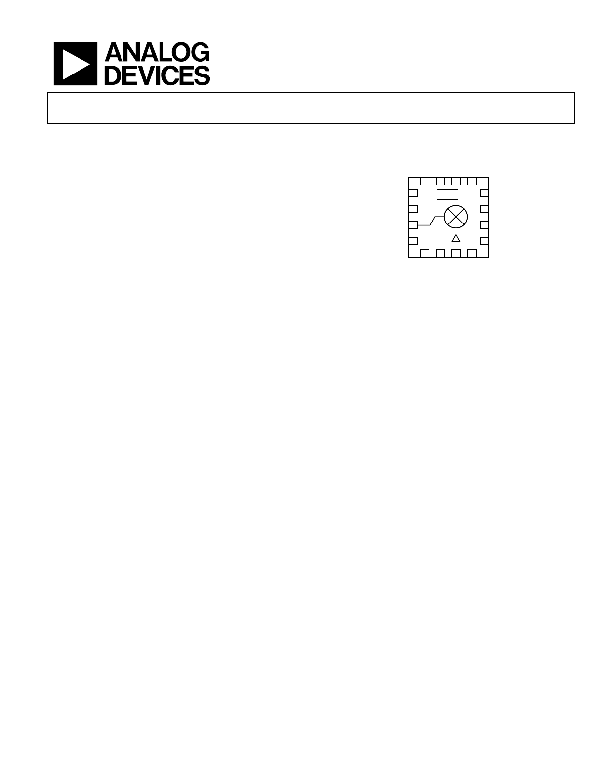
AD8344
FUNCTIONAL BLOCK DIAGRAM
VPDC12PWDN11EXRB10COMM
13
COMM
RFCM
RFIN
VPMX
BIAS
14
15
16
1
2
VPLO
Figure 1.
LOCM
3
LOIN
9
4
COMM
8
7
6
5
COMM
IFOP
IFOM
COMM
04826-0-001
GENERAL DESCRIPTION
The AD8344 is a high performance, broadband active mixer. It
is well suited for demanding receive-channel applications that
require wide bandwidth on all ports and very low intermodulation distortion and noise figure.
The AD8344 provides a typical conversion gain of 4.5 dB at
890 MHz. The integrated LO driver supports a 50 Ω input
impedance with a low LO drive level, helping to minimize
external component count.
The single-ended 50 Ω broadband RF port allows for easy
interfacing to both active devices and passive filters. The RF
input accepts input signals as large as 1.7 V p-p or 8.5 dBm
(re: 50 Ω) at P1dB.
The open-collector differential outputs provide excellent
balance and can be used with a differential filter or IF amplifier,
such as the AD8369 or AD8351. These outputs may also be converted to a single-ended signal through the use of a matching
network or a transformer (balun). When centered on the VPOS
supply voltage, each of the differential outputs may swing
2.5 V p-p.
The AD8344 is fabricated on an Analog Devices proprietary,
high performance SiGe IC process. The AD8344 is available
in a 16-lead LFCSP package. It operates over a −40°C to +85°C
temperature range. An evaluation board is also available.
Rev. 0
Information furnished by Analog Devices is believed to be accurate and reliable.
However, no responsibility is assumed by Analog Devices for its use, nor for any
infringements of patents or other rights of third parties that may result from its use.
Specifications subject to change without notice. No license is granted by implication
or otherwise under any patent or patent rights of Analog Devices. Trademarks and
registered trademarks are the property of their respective owners.
One Technology Way, P.O. Box 9106, Norwood, MA 02062-9106, U.S.A.
Tel: 781.329.4700
Fax: 781.326.8703 © 2004 Analog Devices, Inc. All rights reserved.
www.analog.com
Page 2

AD8344
TABLE OF CONTENTS
Specifications..................................................................................... 3
IF Port.......................................................................................... 14
AC Performance ............................................................................... 4
Absolute Maximum Ratings............................................................ 5
ESD Caution.................................................................................. 5
Pin Configuration and Function Descriptions............................. 6
Typical Performance Characteristics............................................. 7
Circuit Description......................................................................... 13
AC Interfaces ................................................................................... 14
REVISION HISTORY
6/04—Revision 0: Initial Version
LO Considerations ..................................................................... 15
Bias Resistor Selection ............................................................... 16
Conversion Gain and IF Loading............................................. 16
Low IF Frequency Operation.................................................... 17
Evaluation Board ............................................................................ 18
Outline Dimensions....................................................................... 20
Ordering Guide .......................................................................... 20
Rev. 0 | Page 2 of 20
Page 3

AD8344
SPECIFICATIONS
VS = 5 V, TA = 25°C, fRF = 890 MHz, fLO = 1090 MHz, LO power = 0 dBm, ZO = 50 Ω, R
Table 1.
Parameter Conditions Min Typ Max Unit
RF INPUT INTERFACE (Pin 15, RFIN and Pin 14, RFCM)
Return Loss 10 dB
DC Bias Level Internally generated; port must be ac-coupled 2.6 V
OUTPUT INTERFACE
Output Impedance Differential impedance, f = 200 MHz 9||1 kΩ||pF
DC Bias Voltage Externally generated 4.75 VS 5.25 V
Power Range Via a 4:1 balun 13 dBm
LO INTERFACE
LO Power −10 0 +4 dBm
Return Loss 10 dB
DC Bias Voltage Internally generated; port must be ac-coupled VS − 1.6 V
POWER-DOWN INTERFACE
PWDN Threshold VS − 1.4 V
PWDN Response Time Device enabled, IF output to 90% of its final level 0.4 µs
Device disabled, supply current < 5 mA 0.01 µs
PWDN Input Bias Current Device enabled −80 µA
Device disabled 100 µA
POWER SUPPLY
Positive Supply Voltage 4.75 V
Quiescent Current
VPDC Supply current for bias cells 5 mA
VPMX, IFOP, IFOM Supply current for mixer, R
VPLO Supply current for LO limiting amplifier 35 mA
Total Quiescent Current 73 84 95 mA
Power-Down Current Device disabled 500 µA
= 2.43 kΩ 44 mA
BIAS
= 2.43 kΩ, unless otherwise noted.
BIAS
S
5.25 V
Rev. 0 | Page 3 of 20
Page 4

AD8344
AC PERFORMANCE
VS = 5 V, TA = 25°C, LO power = 0 dBm, ZO = 50 Ω, R
Table 2.
Parameter Conditions Min Typ Max Unit
RF Frequency Range 400 1200 MHz
LO Frequency Range High Side LO 470 1600 MHz
IF Frequency Range 70 400 MHz
Conversion Gain fRF = 450 MHz, fLO = 550 MHz, fIF = 100 MHz 9.25 dB
f
= 890 MHz, fLO = 1090 MHz, fIF = 200 MHz 4.5 dB
RF
SSB Noise Figure fRF = 450 MHz, fLO = 550 MHz, fIF = 100 MHz 7.75 dB
f
Input Third-Order Intercept
Input Second-Order Intercept f
f
= 890 MHz, fLO = 1090 MHz, fIF = 200 MHz 10.5 dB
RF
= 450 MHz, f
f
RF1
f
= 100 MHz, each RF tone = −10 dBm
IF
= 890 MHz, f
f
RF1
= 200 MHz, each RF tone = −10 dBm
f
IF
= 450 MHz, f
RF1
= 890 MHz, f
RF1
Input 1 dB Compression Point fRF = 450 MHz, fLO = 550 MHz, fIF = 100 MHz 2.5 dBm
f
= 890 MHz, fLO = 1090 MHz, fIF = 200 MHz 8.5 dBm
RF
LO to IF Output Feedthrough LO Power = 0 dBm, fRF = 890 MHz, fLO = 1090 MHz −23 dBc
LO to RF Input Leakage LO Power = 0 dBm, fRF = 890 MHz, fLO = 1090 MHz −48 dBc
RF to IF Output Feedthrough RF Power = −10 dBm, fRF = 890 MHz, fLO = 1090 MHz −32 dBc
IF/2 Spurious RF Power = −10 dBm, fRF = 890 MHz, fLO = 1090 MHz −66 dBm
= 2.43 kΩ, unless otherwise noted.
BIAS
= 451 MHz, fLO = 550 MHz,
RF2
= 891 MHz, fLO = 1090 MHz,
RF2
= 500 MHz, fLO = 550 MHz, fIF = 100 MHz 36 dBm
RF2
= 940 MHz, fLO = 1090 MHz, fIF = 200 MHz 51 dBm
RF2
14 dBm
24 dBm
Rev. 0 | Page 4 of 20
Page 5
AD8344
ABSOLUTE MAXIMUM RATINGS
Table 3.
Parameter Rating
Supply Voltage, VS 5.5 V
RF Input Level 12 dBm
LO Input Level 12 dBm
PWDN Pin VS + 0.5 V
IFOP, IFOM Bias Voltage 5.5 V
Minimum Resistor from EXRB to COMM 2.4 kΩ
Internal Power Dissipation 580 mW
θJA 77°C/W
Maximum Junction Temperature 125°C
Operating Temperature Range −40°C to +85°C
Storage Temperature Range −65°C to +150°C
Lead Temperature Range (Soldering 60 sec) 300°C
ESD CAUTION
ESD (electrostatic discharge) sensitive device. Electrostatic charges as high as 4000 V readily accumulate
on the human body and test equipment and can discharge without detection. Although this product features
proprietary ESD protection circuitry, permanent damage may occur on devices subjected to high energy
electrostatic discharges. Therefore, proper ESD precautions are recommended to avoid performance
degradation or loss of functionality.
Stresses above those listed under Absolute Maximum Ratings
may cause permanent damage to the device. This is a stress rating only; functional operation of the device at these or any
other conditions above those indicated in the operational section of this specification is not implied. Exposure to absolute
maximum rating conditions for extended periods may affect
device reliability.
Rev. 0 | Page 5 of 20
Page 6
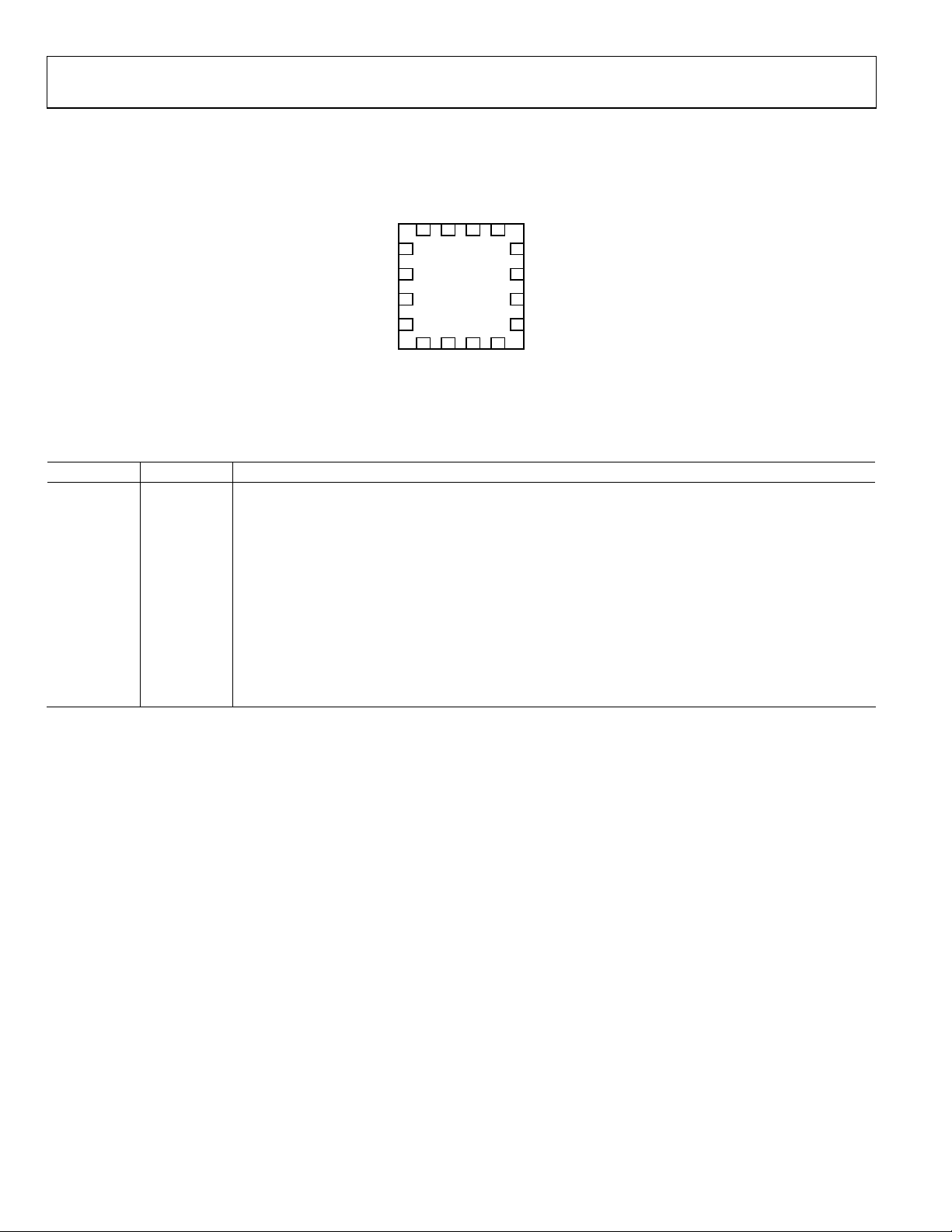
AD8344
PIN CONFIGURATION AND FUNCTION DESCRIPTIONS
COMM
RFCM
RFIN
VPMX
VPDC12PWDN11EXRB10COMM
13
14
15
16
1
2
VPLO
LOCM
3
LOIN
9
4
COMM
8
7
6
5
COMM
IFOP
IFOM
COMM
04826-0-002
Figure 2. 16-Lead LFCSP
Table 4. Pin Function Descriptions
Pin No. Mnemonic Function
1 VPLO Positive Supply Voltage for the LO Buffer: 4.75 V to 5.25 V.
2 LOCM AC Ground for Limiting LO Amplifier, AC-Coupled to Ground.
3 LOIN LO Input. Nominal input level 0 dBm, input level range −10 dBm to +4 dBm, re: 50 Ω, ac-coupled.
4, 5, 8, 9, 13 COMM Device Common (DC Ground).
6, 7 IFOM, IFOP Differential IF Outputs; Open Collectors, Each Requires DC Bias of 5.00 V (Nominal).
10 EXRB
Mixer Bias Voltage, Connect Resistor from EXRB to Ground, Typical Value of 2.43 kΩ
Sets Mixer Current to Nominal Value. Minimum resistor value from EXRB to ground = 2.4 kΩ.
11 PWDN Connect to Ground for Normal Operation. Connect pin to VS for disable mode.
12 VPDC Positive Supply Voltage for the DC Bias Cell: 4.75 V to 5.25 V.
14 RFCM AC Ground for RF Input, AC-Coupled to Ground.
15 RFIN RF Input. Must be ac-coupled.
16 VPMX Positive Supply Voltage for the Mixer: 4.75 V to 5.25 V.
Rev. 0 | Page 6 of 20
Page 7

AD8344
TYPICAL PERFORMANCE CHARACTERISTICS
12
10
8
6
4
GAIN (dB)
2
0
–2
400 500 600 700 800 900 1000 1100 1200
RF FREQUENCY (MHz)
Figure 3. Conversion Gain vs. RF Frequency
6.0
5.5
5.0
4.5
4.0
3.5
3.0
2.5
GAIN (dB)
2.0
1.5
1.0
0.5
0
–10–9–8–7–6–5–4–3–2–101234
Figure 4. Conversion Gain vs. LO Power, F
7.0
6.5
6.0
5.5
5.0
4.5
GAIN (dB)
4.0
3.5
3.0
2.5
2.0
–40 80706050403020100–10–20–30
Figure 5. Conversion Gain vs. Temperature, F
LO LEVEL (dBm)
= 890 MHz, FIF = 200 MHz
RF
TEMPERATURE (°C)
RF
= 890 MHz, FLO = 1090 MHz
IF = 70MHz
IF = 100MHz
IF = 200MHz
IF = 400MHz
VS = 4.75V
VS = 5.0V
VS = 5.25V
04826-0-010
04826-0-022
04826-0-018
10
9
8
7
6
5
GAIN (dB)
4
3
2
1
0
80 120 160 200 240 280 320 360 400
IF FREQUENCY (MHz)
RF = 450MHz
RF = 890MHz
Figure 6. Conversion Gain vs. IF Frequency
45
40
35
30
25
20
PERCENTAGE
15
10
5
0
3.6 3.8 4.0 4.2 4.4 4.6 4.8 5.0 5.2 5.4
GAIN (dB)
Figure 7. Conversion Gain Distribution, F
NORMAL (MEAN = 4.47,
STD DEV = 0.18)
GAIN PERCENTAGE
= 890 MHz, FIF = 200 MHz
RF
04826-0-011
04826-0-031
Rev. 0 | Page 7 of 20
Page 8

AD8344
28
26
24
22
20
18
INPUT IP3 (dBm)
16
14
12
10
Figure 8. Input IP3 vs. RF Frequency (RF Tone Spacing = 1 MHz)
25.0
24.5
24.0
23.5
23.0
22.5
22.0
INPUT IP3 (dBm)
21.5
21.0
20.5
20.0
30
29
28
27
26
25
24
INPUT IP3 (dBm)
23
22
21
20
IF = 70MHz
IF = 100MHz
IF = 200MHz
IF = 400MHz
400 500 600 700 800 900 1000 1100 1200
–10–9–8–7–6–5–4–3–2–101234
RF FREQUENCY (MHz)
LO LEVEL (dBm)
Figure 9. Input IP3 vs. LO Power,
F
–40 80706050403020100–10–20–30
= 890 MHz, F
RF1
= 891 MHz, FLO = 1090 MHz
RF2
TEMPERATURE (°C)
Figure 10. Input IP3 vs. Temperature,
= 890 MHz, F
F
RF1
= 891 MHz, FLO = 1090 MHz
RF2
VS = 4.75V
VS = 5.0V
VS = 5.25V
04826-0-012
04826-0-023
04826-0-019
30
28
26
24
22
20
18
INPUT IP3 (dBm)
16
14
12
10
80 120 160 200 240 280 320 360 400
RF = 890MHz
RF = 450MHz
IF FREQUENCY (MHz)
Figure 11. Input IP3 vs. IF Frequency (RF Tone Spacing = 1 MHz)
35
30
25
20
15
PERCENTAGE
10
5
0
23.0 23.2 23.4 23.6 23.8 24.0 24.2 24.4 24.6 25.024.8
INPUT IP3 (dBm)
NORMAL (MEAN = 24.023,
STD DEV = 0.24)
IP3 PERCENTAGE
Figure 12. Input IP3 Distribution,
= 890 MHz, F
F
RF1
= 891 MHz, FLO = 1090 MHz
RF2
04826-0-013
04826-0-032
Rev. 0 | Page 8 of 20
Page 9

AD8344
50
48
46
44
42
40
38
INPUT IP2 (dBm)
36
34
32
30
400 500 600 700 800 900 1000 1100 1200
RF FREQUENCY (MHz)
IF = 70
IF = 100
IF = 200
IF = 400
Figure 13. Input IP2 vs. RF Frequency (RF Tone Spacing = 50 MHz)
60
58
56
54
52
50
48
46
44
42
40
INPUT IP2 (dBm)
38
36
34
32
30
–10–9–8–7–6–5–4–3–2–1 0 1 2 3 4
LO LEVEL (dBm)
Figure 14. Input IP2 vs. LO Power,
F
= 890 MHz, FLO = 1090 MHz (RF Tone Spacing = 50 MHz)
RF
54
52
4.75V
5.0V
5.25V
04826-0-033
04826-0-034
60
58
56
54
52
50
48
46
44
42
INPUT IP2 (dBm)
40
38
36
34
32
30
80 120 160 200 240 280 320 360 400
IF FREQUENCY (MHz)
RF = 890MHz
RF = 450MHz
Figure 16. Input IP2 vs. IF Frequency (RF Tone Spacing = 50 MHz)
35
30
25
20
15
PERCENTAGE
10
5
0
44 45 46 47 48 49 50 51 52 555453
INPUT IP2 (dBm)
Figure 17. Input IP2 Distribution, F
NORMAL (MEAN = 48.96,
STD DEV = 01.17)
IIP2 PERCENTAGE
= 890 MHz,
RF
FLO = 1090 MHz (RF Tone Spacing = 50 MHz)
04826-0-015
04826-0-035
50
48
46
INPUT IP2 (dBm)
44
42
40
–40–30–20–100 1020304050607080
Figure 15. Input IP2 vs. Temperature, F
TEMPERATURE (°C)
= 890 MHz,
RF
FLO = 1090 MHz (RF Tone Spacing = 50 MHz)
04826-0-037
Rev. 0 | Page 9 of 20
Page 10

AD8344
12
10
INPUT P1dB (dBm)
9.0
8.8
8.6
8.4
8.2
8.0
7.8
INPUT P1dB (dBm)
7.6
7.4
7.2
7.0
Figure 19. Input P1dB vs. LO Power, F
10.0
9.5
9.0
8.5
8.0
7.5
7.0
INPUT P1dB (dBm)
6.5
6.0
5.5
5.0
Figure 20. Input P1dB vs. Temperature, F
IF = 70MHz
IF = 100MHz
IF = 200MHz
IF = 400MHz
8
6
4
2
0
400 500 600 700 800 900 1000 1100 1200
RF FREQUENCY (MHz)
Figure 18. Input P1dB vs. RF Frequency
–10–9–8–7–6–5–4–3–2–101234
–40 80706050403020100–10–20–30
TEMPERATURE (°C)
LO LEVEL (dBm)
= 890 MHz, FLO = 1090 MHz
RF
= 890 MHz, FLO = 1090 MHz
RF
VS = 4.75V
VS = 5.0V
VS = 5.25V
04826-0-016
04826-0-024
04826-0-020
10
9
8
7
6
5
4
INPUT P1dB (dBm)
3
2
1
0
80 120 160 200 240 280 320 360 400
IF FREQUENCY (MHz)
RF = 890MHz
RF = 450MHz
Figure 21. Input P1dB vs. IF Frequency
60
NORMAL (MEAN = 8.50,
55
50
45
40
35
30
25
PERCENTAGE
20
15
10
5
0
7.0 7.5 8.0 8.5 9.0 9.5 10.0
Figure 22. Input P1dB Distribution, F
STD DEV = 0.38)
INPUT P1dB PERCENTAGE
INPUT P1dB (dBm)
= 890 MHz, FLO = 1090 MHz
RF
04826-0-017
04826-0-036
Rev. 0 | Page 10 of 20
Page 11

AD8344
25
INPUT IP3
20
15
10
NF AND IP3 (dBm)
5
0
2.4 2.6 2.8 3.0 3.2 3.4 3.6 3.8 4.0
CURRENT
NOISE FIGURE
R
BIAS
(kΩ)
Figure 23. Noise Figure, Input IP3 and Supply Current vs. R
F
= 891 MHz, FLO = 1090 MHz
RF2
14
13
12
11
10
9
8
NOISE FIGURE SSB (dBm)
7
6
400 500 600 700 800 900 1000 1100 1200
RF FREQUENCY (MHz)
Figure 24. Noise Figure vs. RF Frequen cy
13.5
13.0
12.5
12.0
11.5
11.0
NOISE FIGURE SSB (dBm)
10.5
10.0
–15–13–11–9–7–5–3–1 1 3 5
Figure 25. Noise Figure vs. LO Power, F
LO POWER (dBm)
= 890 MHz, FLO = 1090 MHz
RF
BIAS
, F
= 890 MHz,
RF1
IF = 70
IF = 100
IF = 200
IF = 400
100
95
90
85
80
75
70
65
60
55
50
SUPPLY CURRENT (mA)
04826-0-026
04826-0-027
04826-0-029
14
12
10
8
6
4
INPUT P1dB (dBm)
2
0
–2
2.4 2.6 2.8 3.0 3.2 3.4 3.6 3.8 4.0
Figure 26. Input P1dB vs. R
11.0
10.5
10.0
9.5
9.0
8.5
8.0
7.5
NOISE FIGURE SSB (dBm)
7.0
6.5
6.0
70 100 150 200 250 300 350 400
R
(kΩ)
BIAS
= 890 MHz, FLO = 1090 MHz
BIAS, FRF
890MHz
450MHz
IF FREQUENCY (MHz)
Figure 27. Noise Figure vs. IF Frequen cy
100
95
90
85
80
75
CURRENT (mA)
70
65
60
–40 80706050403020100–10–20–30
TEMPERATURE (°C)
Figure 28. Total Supply Current vs. Temperature
04826-0-025
04826-0-028
VS = 4.75V
VS = 5.0V
VS = 5.25V
04826-0-021
Rev. 0 | Page 11 of 20
Page 12

AD8344
90
90
120
150
400MHz
210
240
270
60
1.2GHz
300
Figure 29. RFIN Return Loss vs. RF Frequency
0
–5
–10
–15
–20
–25
–30
FEEDTHROUGH (dBc)
–35
–40
–45
400 500 600 700 800 900 1000 1100 1200
RF FREQUENCY (MHz)
Figure 30. RF to IF Feedthrough vs. RF Frequency,
= 1090 MHz, RF Power = −10 dBm
F
LO
0
30
330
0180
04826-0-051
04826-0-053
120
150
1.6GHz
400MHz
210
240
270
60
30
0180
330
300
Figure 32. LOIN Return Loss vs. LO Frequency
0
–5
–10
–15
–20
–25
FEEDTHROUGH (dBc)
–30
–35
–40
400 600 800 1000 1200 1400 1600
LO FREQUENCY (MHz)
Fig ure 3 3. LO t o IF Fe edth roug h vs. LO Fr eque ncy, LO Po wer = 0 dBm
14000
3.0
04826-0-052
04826-0-054
–10
–20
–30
–40
–50
LEAKAGE (dBc)
–60
–70
–80
400 600 800 1000 1200 1400 1600
LO FREQUENCY (MHz)
Fig ure 3 1. LO t o RF Leak age v s. LO Fr eque ncy, LO Po wer = 0 dBm
04826-0-055
Rev. 0 | Page 12 of 20
12000
10000
RESISTANCE (Ω)
8000
6000
4000
2000
70 370320270220170120
FREQUENCY (MHz)
2.5
2.0
1.5
1.0
0.5
0
Figure 34. IF Port Output Resistance and Capacitance vs. IF Frequency
CAPACITANCE (pF)
04826-0-030
Page 13

AD8344
CIRCUIT DESCRIPTION
The AD8344 is a down converting mixer optimized for operation within the input frequency range of 400 MHz to 1.2 GHz. It
has a single-ended, 50 Ω RF input, as well as a single-ended,
50 Ω local oscillator (LO) input. The IF outputs are differential
open collectors. The mixer current can be adjusted by the value
of an external resistor to optimize performance for gain compression and intermodulation or for low power operation.
Figure 35 shows the basic blocks of the mixer, which includes
the LO buffer, RF voltage-to-current converter, bias cell, and
mixing core.
The RF voltage to RF current conversion is done via an
inductively degenerated differential pair. When one side of the
differential pair is ac grounded, the other input can be driven
single-ended. The RF inputs can also be driven differentially.
The voltage-to-current converter then drives the emitters of a
four-transistor switching core. This switching core is driven by
an amplified version of the local oscillator signal connected to
the LO input. There are three limiting gain stages between the
external LO signal and the switching core. The first stage converts the single-ended LO drive to a well balanced differential
drive. The differential drive then passes through two more gain
stages, which ensures a limited signal drives the switching core.
This affords the user a lower LO drive requirement, while
maintaining excellent distortion and compression performance.
The output signal of these three LO gain stages drives the four
transistors within the mixer core to commutate at the rate of th
local oscillator frequency. The output of the mixer core is taken
directly from these open collectors. The open collector outputs
present a high impedance at the IF frequency. The conversion
gain of the mixer depends directly on the impedance presented
to these open collectors. In characterization, a 200 Ω load was
presented to the part via a 4:1 impedance transformer.
The AD8344 also features a power-down function.
Application of a logic low at the PWDN pin allows normal
operation. A high logic level at the PWDN pin shuts down the
AD8344. Power consumption when the part is disabled is less
than 10 mW.
The bias for the mixer is set with an external resistor from the
EXRB pin to ground. The value of this resistor directly affects
the dynamic range of the mixer. The external resistor should not
be lower than 2.4 kΩ. Permanent damage to the part will result
if values below 2.4 kΩ are used.
VPMX
RFIN
RFCM
Figure 35. AD8344 Simplified Schematic
As shown in Figure 36, the IF output pins, IFOP and IFOM, are
directly connected to the open collectors of the NPN transistors
in the mixer core so the differential and single-ended impedances looking into this port are relatively high, on the order of
several kΩ. A connection between the supply voltage and these
output pins is required for proper mixer core operation.
IFOP IFOM
e
Figure 36. Mixer Core Simplified Schematic
The AD8344 has three pins for the supply voltage: VPDC,
VPMX, and VPLO. These pins are separated to minimize or
eliminate possible parasitic coupling paths within the AD8344
that could cause spurious signals or reduced interport isolation.
Consequently, each of these pins should be well bypassed and
decoupled as close to the AD8344 as possible.
EXTERNAL
BIAS
RESISTORVPDC PWDN
BIAS
SE
TO
DIFF
INPUT
COMM
LO
VPLO
IFOP
IFOM
RFCMRFIN
04826-0-003
LOIN
04826-0-003
Rev. 0 | Page 13 of 20
Page 14

AD8344
AC INTERFACES
The AD8344 is a high-side downconverter. It is designed to
downconvert radio frequencies (RF) to lower intermediate
frequencies (IF) using a high-side local oscillator (LO). The LO
is injected into the mixer core at a frequency greater than the
desired input RF frequency. The difference between the LO and
− f
RF frequencies, f
the desired RF signal, an RF image will be downconverted to the
same IF frequency. The image frequency is at f
version gain of the AD8344 decreases with increasing input
frequency. By choosing to use a high-side LO the image frequency at f
+ fIF is translated with less conversion gain than
LO
the desired RF signal at f
noise present at the image frequency will be downconverted
with less conversion gain than would be the case if a low-side
LO was applied. In general, a high-side LO should be used with
the AD8344 to ensure optimal noise performance and image
rejection.
The AD8344 is designed to operate using RF frequencies in the
400 MHz to 1200 MHz frequency range, with high-side LO
injection within the 470 MHz to 1600 MHz range. It is essential
to ac-couple RF and LO ports to prevent dc offsets from skewing the mixer core in an asymmetrical manner, potentially
degrading linear input swing and impacting distortion and
input compression characteristics.
The AD8344 RFIN port presents a 50 Ω impedance relative to
RFCM. In order to ensure a good impedance match, the RFIN
ac-coupling capacitor should be large enough in value so that
the presented reactance is negligible at the intended RF frequency. Addit ionally, the RFCM byp assing cap acitor should be
sufficiently large to provide a low impedance return path to
board ground. Low inductance ceramic grade capacitors of no
more than 330 pF are sufficient for most applications.
Similarly the LOIN port provides a 50 Ω load impedance with
common-mode decoupling on LOCM. Again, common grade
ceramic capacitors will provide sufficient signal coupling and
bypassing of the LO interface.
is the IF frequency, fIF. In addition to
LO
RF,
− fIF. Additionally, any wideband
LO
+ fIF. The con-
LO
90
120
150
210
240
270
60
500MHz
300
10MHz
30
330
0180
04826-0-040
Figure 37. IF Port Reflection Coefficient from 10 MHz to 500 MHz
IF PORT
The IF port uses an open collector differential output interface.
The NPN open collectors can be modeled as high impedance
current sources. The stray capacitance associated with the IC
package presents a slightly capacitive source impedance as in
Figure 37. In general, the IFOP and IFOM output ports can be
modeled as current sources with an impedance of ~10 kΩ in
parallel with ~1 pF of shunt capacitance. Circuit board traces
connecting the IF outputs to the load should be narrow and
short to prevent excessive capacitive loading. In order to maintain the specified conversion gain of the mixer, the IF output
ports should be loaded into 200 Ω. It is not necessary to attempt
to provide a conjugate match to the IF port output source
impedance. If the IF signal needs to be delivered to a remote
load, more than a few centimeters away, it may be necessary to
use an appropriate buffer amplifier to present a real 200 Ω loading impedance at the IF output interface. The buffer amplifier
should have the appropriate source impedance to match the
characteristic impedance of the selected transmission line. An
example is provided in Figure 38, where the AD8351 differential
amplifier is used to drive a pair of 75 Ω transmission lines. The
gain of the buffer can be independently set by choosing an
appropriate gain resistor, R
V
+
S
AD8344
8
COMM
IFOP
IFOM
COMM
R
C
F
7
6
5
200Ω R
R
C
F
.
G
V
+
S
+
AD8351
G
–
Tx LINE ZO = 75Ω
Tx LINE ZO = 75Ω
Z
L
Figure 38. AD8351 Used as Transmission Line Driver and Impedance Buffer
Rev. 0 | Page 14 of 20
V
+
S
Ω
0
0
Z
2
=
L
04826-0-041
Page 15

AD8344
The high input impedance of the AD8351 allows for a shunt
differential termination to provide the desired 200 Ω load to the
AD8344 IF output port.
It is necessary to bias the open collector outputs using one of
the schemes presented in Figure 39 and Figure 40. Figure 39
illustrates the application of a center-tapped impedance transformer. The turns ratio of the transformer should be selected to
provide the desired impedance transformation. In the case of a
50 Ω load impedance, a 4-to-1 impedance ratio transformer
should be used to transform the 50 Ω load into a 200 Ω
differential load at the IF output pins. Figure 40 illustrates a
differential IF interface where pull-up choke inductors are used
to bias the open-collector outputs. The shunting impedance of
the choke inductors used to couple dc current into the mixer
core should be large enough at the IF frequency of operation as
to not load down the output current before reaching the
intended load. Additionally, the dc current handling capability
of the selected choke inductors needs to be at least 45 mA. The
self resonant frequency of the selected choke should be higher
than the intended IF frequency. A variety of suitable choke
inductors are commercially available from manufacturers such
as Murata and Coilcraft. An impedance transforming network
may be required to transform the final load impedance to 200 Ω
at the IF outputs. There are several good reference books that
explain general impedance matching procedures, including:
• Chris Bowick, RF Circuit Design, Newnes, Reprint E dition,
1997.
• David M. Pozar, Microwave Engineering, Wiley Text Books,
Second Edition, 1997.
• Guillermo Gonzalez, Microwave Transistor Amplifiers: Analy-
sis and Design, Prentice Hall, Second Edition, 1996.
V
+
S
AD8344
COMM
IFOP
IFOM
COMM
8
7
6
5
ZL
4:1
Ω
0
0
2
=
Figure 39. Biasing the IF Port Open Collector Outputs
Using a Center-Tapped Impedance Transformer
V
+
S
AD8344
COMM
8
R
C
IFOP
IFOM
COMM
F
7
6
5
Z
L
R
C
F
V
+
S
U
I
+
F
T
O
Ω
0
0
2
=
U
I
–
F
T
O
Figure 40. Biasing the IF Port Open Collector Outputs
Using Pull-Up Choke Inductors
IF
OUT
Z
0
5
=
O
IMPEDANCE
TRANSFORMING
NETWORK
Ω
04826-0-042
Z
L
04826-0-043
90
120
150
210
240
270
60
50MHz
500MHz
500MHz
300
30
330
REAL
CHOKES
0180
50MHz
IDEAL
CHOKES
04826-0-044
Figure 41. IF Port Loading Effects due to Finite-Q Pull-Up Inductors
(Murata BLM18HD601SN1D Chokes)
LO CONSIDERATIONS
The LO signal needs to have adequate phase noise characteristics and reasonable low second harmonic content to prevent
degradation of the noise figure performance of the AD8344. A
LO plagued with poor phase noise can result in reciprocal
mixing, a mechanism that causes spectral spreading of the
downconverted signal, limiting the sensitivity of the mixer at
frequencies close-in to any large input signals. The internal LO
buffer provides enough gain to hard limit the input LO and
provide fast switching of the mixer core. Odd harmonic content
present on the LO drive signal should not impact mixer
performance; however, even-order harmonics cause the mixer
core to commutate in an unbalanced manner, potentially
degrading noise performance. Simple lumped element low-pass
filtering can be applied to help reject the harmonic content of a
given local oscillator, as illustrated in Figure 42. The filter
depicted is a common 3-pole Chebyshev, designed to maintain a
1-to-1 source-to-load impedance ratio with no more than
0.5 dB of ripple in the pass band. Other filter structures can be
effective as long as the second harmonic of the LO is filtered to
negligible levels, e.g., ~30 dB below the fundamental. The measured frequency response of the Chebyshev filter for a 1200 MHz
−3 dB cutoff frequency is presented in Figure 43.
AD8344
LOIN3COMM
LOCM
L2
1.28R
2
πf
2
L
L
C3 =
c
R
S
LO
SOURCE
C1 =
f
- FILTER CUTOFF FREQUENCY
C
1.864
πf
2
R
c
L
C1 C3
FOR RS= R
L2 =
Figure 42. Using a Low-Pass Filter to Reduce LO Second Harmonic
R
L
1.834
πf
2
4
R
c
L
04826-0-045
Rev. 0 | Page 15 of 20
Page 16

AD8344
g
0
–5
–10
–15
–20
–25
–30
RESPONSE (dB)
–35
–40
4.7pF 4.7pF
–45
–50
0.1 1 10
6.8nH
REAL LPF
FREQUENCY (GHz)
IDEAL LPF
04826-0-046
Figure 43. Measured and Id eal LO Filter Frequenc y Respons e
BIAS RESISTOR SELECTION
An external bias resistor is used to set the dc current in the
mixer core. This provides the ability to reduce power consumption at the expense of decreased dynamic range. Figure 44
shows the spurious-free dynamic range (SFDR) of the mixer for
a 1 Hz noise bandwidth versus the R
was calculated using NF and IIP3 data collected at 900 MHz.
By definition,
2
()
3
where IIP3 is the input third-order intercept in dBm. NF is the
noise figure in dB. kT is the thermal noise power density and is
−173.86 dBm/Hz at 298°K. B is the noise bandwidth in Hz.
In order to calculate the anticipated SFDR for a given application, it is necessary to factor in the actual noise bandwidth. For
instance, if the IF noise bandwidth was 5 MHz, the anticipated
SFDR using a 2.43 kΩ R
would be 6.66 log10 (5 MHz) less
BIAS
than the 1 Hz data in Figure 44 or ~80 dBc. Using a 2.43 kΩ bias
resistor will set the quiescent power dissipation to ~415 mW for
a 5 V supply. If the R
resistor value was raised to 3.9 kΩ, the
BIAS
SFDR for the same 5 MHz bandwidth would be reduced to
~77.5 dBc and the power dissipation would be reduced to
~335 mW. In low power portable applications it may be advantageous to reduce power consumption by using a larger value of R
assuming reduced dynamic range performance is acceptable.
resistor value. SFDR
BIAS
)(10log
BkTNFIIP3SFDR −−−=
BIAS
125
124
123
+V
S
122
SFDR (dBc)
121
12
PWDN
VPDC
120
2.4 2.6 2.8 3.0 3.2 3.4 3.6 3.8 4.0
Figure 44. Impact of R
11
EXRB
AD8344
R
BIAS
9
10
COMM
R
(kΩ)
BIAS
Resistor Selection vs. Spurious-Free
BIAS
85
81
77
73
SUPPLY CURRENT (mA)
69
04826-0-047
65
Dynamic Range and Power Consumption,
F
= 890 MHz and FLO = 1090 MHz
RF
CONVERSION GAIN AND IF LOADING
The AD8344 is optimized for driving a 200 Ω differential load.
Although the device is capable of driving a wide variety of
loads, in order to maintain optimum distortion and noise
performance, it is advised that the presented load at the IF
outputs is reasonably close to 200 Ω. Figure 45 illustrates the
effect of IF loading on conversion gain. The mixer outputs
behave like Norton equivalent sources, where the conversion
gain is the effective transconductance of the mixer multiplied
by the loading impedance. The linear differential voltage
conversion gain of the mixer can be modeled as
RAv
LOAD
××−=
where R
0.46
is the differential loading impedance. gm is the
LOAD
mixer transconductance and is equal to 4070/R
frequency of the signal applied to the RF port in GHz.
Large impedance loads cause the conversion gain to increase,
resulting in a decrease in input linearity and allowable signal
swing. In order to maintain positive conversion gain and preserve spurious-free dynamic range performance, the differential
load presented at the IF port should remain within a range of
,
~100 Ω to 250 Ω.
m
×××+
37.701
m
fgj
RF
. fRF is the
BIAS
Rev. 0 | Page 16 of 20
Page 17

AD8344
25
15
15
20
15
10
5
20LOG–CONVERSION GAIN (dB)
0
–5
10 100 1000
MODELED
IF LOADING (Ω)
MEASURED
04826-0-048
Figure 45. Conversion Gain vs. IF Loading Figure 46. Conversion Gain, Input IP3, and P1dB vs.
LOW IF FREQUENCY OPERATION
The AD8344 may be used down to arbitrarily low IF frequencies. The conversion gain, noise, and linearity characteristics
remain quite flat as IF frequency is reduced, as indicated in
Figure 46 and Figure 47. Larger value pull-up inductors need to
be used at the lower IF frequencies. A 1 µH choke inductor
would present a common-mode loading impedance of 63 Ω at
an IF frequency of 10 MHz, severely loading down the mixer
outputs, reducing conversion gain, and sacrificing output power.
At low IF frequencies, choke inductors of several hundred µH
should be used for biasing the IF outputs.
12
9
6
CONVERSION GAIN (dB)
3
0
10 15 20 25 30 35 40 45 50
8
7
6
5
4
CONVERSION GAIN (dB)
3
IF FREQUENCY (MHz)
IF Frequency, F
= 450 MHz
RF
12
9
6
3
0
28.0
24.5
21.0
17.5
14.0
10.5
INPUT IP3 AND P1dB (dBm)
04826-0-049
INPUT IP3 AND P1dB (dBm)
2
10 15 20 25 30 35 40 45 50
IF FREQUENCY (MHz)
7.0
04826-0-050
Figure 47. Conversion Gain, Input IP3, and P1dB vs.
IF Frequency, F
= 890 MHz
RF
Rev. 0 | Page 17 of 20
Page 18

AD8344
EVALUATION BOARD
An evaluation board is available for the AD8344. The evaluation
board is configured for single-ended signaling at the IF output
port via a balun transformer. The schematic for the evaluation
board is presented in Figure 48.
Table 5. Evaluation Boards Configuration Options
Component Function Default Conditions
R1, R2, R7,
C2, C4, C5, C6,
C12, C13, C14,
C15
R3, R4 Jumpers in Single-Ended IF Output Circuit. 0 Ω (Size 0603)
R6, C11
R8 Jumper for pull down of the PWDN pin. R8 = 10 kΩ (Size 0603)
R9 Jumper. R9 = 0 Ω (Size 0603)
C3
C1
C8
C7
SW1
T1
R11, Z3, Z4
R12, Z1, Z2
Supply Decoupling.
Jumpers or power supply decoupling resistors and filter capacitors.
resistor that sets the bias current for the mixer core.
R
BIAS
The capacitor provides ac bypass for R6.
RF Input AC Coupling. Provides dc block for RF input.
RF Common AC Coupling. Provides dc block for RF input common connection.
LO Input AC Coupling. Provides dc block for the LO input.
LO Common AC Coupling. Provides dc block for LO input common connection.
Power Down. The part is on when the PWDN is connected to ground via SW1.
The part is disabled when PWDN is connected to the positive supply (V
IF Output Balun Transformer. Converts differential, high impedance IF output
to single-ended. When loaded with 50 Ω, this balun presents a 200 Ω load to the
mixers collectors. The center tap of the primary is used to supply the bias voltage
(V
) to the IF output pins.
S
IF Output Interface—IFOP, IFOM. These positions can be used to modify the
impedance presented to the IF outputs.
R1, R2, R7 = 0 Ω (Size 0603)
C4, C6, C13, C14 = 100 pF
(Size 0603)
C2, C5, C12, C15 = 0.1 µF
(Size 0603)
R6 = 2.43 kΩ (Size 0603)
C11 = 100 pF (Size 0603)
C3 = 100 pF (Size 0402)
C1 = 100 pF (Size 0402)
C8 = 100 pF (Size 0402)
C7 = 100 pF (Size 0402)
) via SW1.
S
T1 = TC4-1W, 4:1 (Mini-Circuits)
R11 = 0 Ω (Size 0603)
Z3, Z4 = Open
R12 = 0 Ω (Size 0603)
Z1, Z2 = Open
Rev. 0 | Page 18 of 20
Page 19

AD8344
POWER
VPOS
RF INPUT
VPOS
C12
0.1µF
0.1µF
100pF
C2
0.1µF
DOWN
R7
0Ω
C13
100pF
COMM
C1
100pF
C4
100pF
RFCM
RFIN
VPMX
C6
C3
R1
0Ω
100pF
R2
0Ω
C5
R8
10kΩ
VPDC
VPLO
100pF
SW1
C7
R9
0Ω
PWDN
AD8344
LOCM
C11
100pF
R6
2.43kΩ
EXRB
LOIN
C8
100pF
LO
INPUT
COMM
COMM
IFOP
IFOM
COMM
COMM
COMMON
Z1
OPEN
R10
0Ω
R11
0Ω
Z3
OPENZ4OPEN
Z2
OPEN
VPOS
R3
0Ω
T1
TC4-1W
C14
100pF
C15
0.1µF
R4
0Ω
IF
OUTPUT
04826-0-005
Figure 48. Evaluation Board Schematic—Single-Ended IF Output
Figure 49. Single-Ended Evaluation Board, Component Side Layout
04826-0-007
Figure 50. Single-Ended Evaluation Board, Component Side Silkscreen
04826-0-008
Rev. 0 | Page 19 of 20
Page 20

AD8344
OUTLINE DIMENSIONS
PIN 1
INDICATOR
1.00
0.85
0.80
SEATING
PLANE
12° MAX
3.00
BSC SQ
TOP VIEW
0.30
0.23
0.18
2.75
BSC SQ
0.80 MAX
0.65 TYP
0.05 MAX
0.02 NOM
0.20 REF
*
COMPLIANTTO JEDEC STANDARDS MO-220-VEED-2
EXCEPT FOR EXPOSED PAD DIMENSION
0.45
0.50
BSC
1.50 REF
0.60 MAX
Figure 51. 16-Lead Lead Frame Chip Scale Package [LFCSP]
3 mm × 3 mm Body (CP-16-3)
Dimensions in millimeters
0.50
0.40
0.30
13
16
BOTTOM
VIEW
1
4
5
12
9
8
PIN 1 INDICATOR
1.65
*
1.50 SQ
1.35
0.25 MIN
ORDERING GUIDE
Models Temperature Range Package Description Package Option Branding
AD8344ACPZ-REEL71−40°C to +85°C 16-Lead Lead Frame Chip Scale Package (LFCSP) CP-16-3 JHA
AD8344ACPZ-WP
AD8344-EVAL Evaluation Board
1
Z = Pb-free part.
2
WP = Waffle pack.
1, 2
−40°C to +85°C 16-Lead Lead Frame Chip Scale Package (LFCSP) CP-16-3 JHA
© 2004 Analog Devices, Inc. All rights reserved. Trademarks and registered trademarks are the property of their respective owners.
D04826–0–6/04(0)
Rev. 0 | Page 20 of 20
 Loading...