

Page 1
DC-to-2.5 GHz
C
C
FEATURES
High-performance active mixer
Broadband operation to 2.5 GHz
Conversion gain: 7 dB
Input IP3: 16.5 dBm
LO drive: –10 dBm
Noise figure: 14 dB
Input P
Differential LO, IF and RF Ports
50 Ω LO input impedance
Single-supply operation: 5 V @ 50 mA typical
Power-down mode @ 20 μA typical
APPLICATIONS
Cellular base stations
Wireless LAN
Satellite converters
SONET/SDH radio
Radio links
RF instrumentation
: 2.8 dBm
1dB
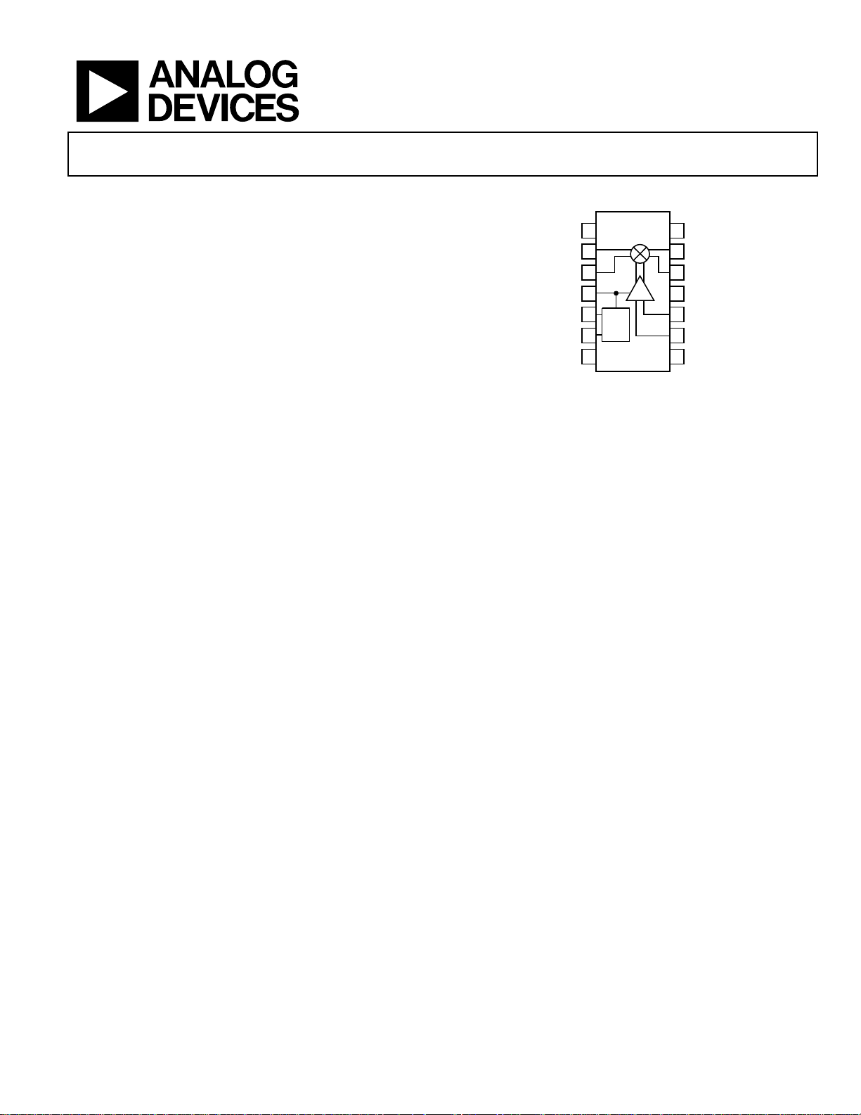
High IP3 Active Mixer
AD8343
FUNCTIONAL BLOCK DIAGRAM
1
2
3
4
5
6
7
AD8343
BIAS
Figure 1.
14
13
12
11
10
9
8
COMM
OUTP
OUTM
COMM
LOIP
LOIM
COMM
01034-001
OMM
INPP
INPM
DCPL
VPOS
PWDN
OMM
GENERAL DESCRIPTION
The AD8343 is a high-performance broadband active mixer.
With wide bandwidth on all ports and very low intermodulation distortion, the AD8343 is well suited for demanding
transmit applications or receive channel applications.
The AD8343 provides a typical conversion gain of 7 dB. The
integrated LO driver supports a 50 Ω differential input impedance with low LO drive level, helping to minimize external
component count.
The open-emitter differential inputs can be interfaced directly
to a differential filter or driven through a balun (transformer)
to provide a balanced drive from a single-ended source.
The open-collector differential outputs can be used to drive a
differential IF signal interface or convert to a single-ended signal
through the use of a matching network or transformer. When
centered on the VPOS supply voltage, the outputs swing ±1 V.
The LO driver circuitry typically consumes 15 mA of current.
Two external resistors are used to set the mixer core current for
required performance, resulting in a total current of 20 mA to
60 mA. This corresponds to power consumption of 100 mW to
300 mW with a single 5 V supply.
The AD8343 is fabricated on Analog Devices, Inc.’s highperformance 25 GHz silicon bipolar IC process. The AD8343 is
available in a 14-lead TSSOP package. It operates over a −40°C
to +85°C temperature range. A device-populated evaluation
board is available.
Rev. B
Information furnished by Analog Devices is believed to be accurate and reliable. However, no
responsibility is assumed by Anal og Devices for its use, nor for any infringements of patents or ot her
rights of third parties that may result from its use. Specifications subject to change without notice. No
license is granted by implication or otherwise under any patent or patent rights of Analog Devices.
Trademarks and registered trademarks are the property of their respective owners.
One Technology Way, P.O. Box 9106, Norwood, MA 02062-9106, U.S.A.
Tel: 781.329.4700 www.analog.com
Fax: 781.461.3113 ©2006 Analog Devices, Inc. All rights reserved.
Page 2

AD8343
TABLE OF CONTENTS
Features.............................................................................................. 1
Applications....................................................................................... 1
Functional Block Diagram ..............................................................1
General Description......................................................................... 1
Revision History ...............................................................................2
Specifications..................................................................................... 3
Basic Operating Instructions ...................................................... 3
Typical AC Performance.............................................................. 4
Typical Isolation Performance.................................................... 4
Absolute Maximum Ratings............................................................ 5
ESD Caution.................................................................................. 5
Pin Configuration and Function Descriptions............................. 6
Simplified Interface Schematics .................................................7
Typical Performance Characteristics............................................. 8
Receiver Characteristics .............................................................. 8
Transmit Characteristics............................................................ 13
Circuit Description......................................................................... 15
DC Interfaces .................................................................................. 16
Biasing and Decoupling (VPOS, DCPL)................................. 16
Power-Down Interface (PWDN) .............................................16
AC Interfaces................................................................................... 17
Input Interface (INPP and INPM)............................................... 18
Single-Ended-to-Differential Conversion............................... 18
Input Matching Considerations ............................................... 18
Input Biasing Considerations ................................................... 19
Output Interface (OUTP, OUTM) ...............................................20
Output Matching Considerations............................................ 20
Output Biasing Considerations ................................................20
Input and Output Stability Considerations................................. 21
Local Oscillator Input Interface (LOIP, LOIM)..................... 22
DC Coupling the LO.................................................................. 22
A Step-by-Step Approach to Impedance Matching............... 23
Applications..................................................................................... 26
Downconverting Mixer............................................................. 26
Upconverting Mixer................................................................... 26
Evaluation Board............................................................................ 27
Outline Dimensions....................................................................... 32
Ordering Guide .......................................................................... 32
REVISION HISTORY
11/06—Rev. A to Rev. B
Changes to General Description .................................................... 1
Changes to Table 1............................................................................ 3
Changes to Table 3............................................................................ 4
Changes to Power-Down Interface (PWDN) Section............... 16
Changes to Output Matching Considerations Section.............. 20
Changes to Circuit Description Section...................................... 15
Changes to Output Matching Considerations............................ 20
Changes to Upconverting Mixer Section .................................... 26
Changes to Table 6, Table 7, and Table 8 .....................................27
Changes to Figure 71 and Figure 72............................................. 29
Updated Outline Dimensions....................................................... 32
Changes to Ordering Guide.......................................................... 32
3/02—Rev. 0 to Rev. A
Edits to Absolute Maximum Ratings..............................................3
Edits to Input Interface (LOIP, LOIM)........................................ 17
Edits to Table III ............................................................................. 22
Edits to Table IV ............................................................................. 23
Edits to Table V............................................................................... 23
Edits to Figure 23............................................................................ 23
Edits to Figure 24............................................................................ 23
6/00—Revision 0—Initial Version
Rev. B | Page 2 of 32
Page 3

AD8343
SPECIFICATIONS
BASIC OPERATING INSTRUCTIONS
VS = 5.0 V, TA = 25°C, unless otherwise noted.
Table 1.
Parameter Conditions/Comments Min Typ Max Unit
INPUT INTERFACE (INPP, INPM)
Differential Open Emitter
DC Bias Voltage Internally generated 1.1 1.2 1.3 V
Operating Current Each Input (IO) Current set by R3, R4; see Figure 72 5 17.6 20 mA
Value of Bias Setting Resistor
Port Differential Impedance f = 50 MHz; R3 and R4 = 68.1 Ω; see Figure 57 5.6 + j 1.4 Ω
OUTPUT INTERFACE (OUTP, OUTM)
Differential Open Collector
DC Bias Voltage Externally applied 4.5 5 5.5 V
Voltage Swing Collector bias (VS) = VPOS 1.65 VS ± 1 VS + 2 V
Operating Current Each Output Same as input current IO mA
Port Differential Impedance f = 50 MHz; see Figure 60 900 − j 77 Ω
LO INTERFACE (LOIP, LOIM)
Differential Common Base Stage
DC Bias Voltage2 Internally generated; (port is typically ac-coupled) 300 360 450 mV
LO Input Power 50 Ω impedance; see Figure 65 −12 −10 −3 dBm
Port Differential Reflection Coefficient See Figure 64 −10 dB
POWER-DOWN INTERFACE (PWDN)
PWDN Threshold Assured on VS − 1.5 V
Assured off VS − 0.5 V
PWDN Response Time3 Time from device on to off; see Figure 52 2.2 μs
Time from device off to on; see Figure 53 500 ns
PWDN Input Bias Current PWDN = 0 V (device on) −160 −250 μA
PWDN = 5 V (device off) 0 μA
POWER SUPPLY
Supply Voltage Range 4.5 5.0 5.5 V
Total Quiescent Current R3 and R4 = 68.1 Ω; see Figure 72 50 60 mA
Over temperature 75 mA
Powered-Down Current VS = 5.5 V 20 95 μA
V
Over temperature; VS = 5.5 V 50 150 μA
1
The balance in the bias current in the two legs of the mixer input is important to applications where a low feedthrough of the local oscillator (LO) is critical.
2
This voltage is proportional to absolute temperature (PTAT). See the DC Coupling the LO section for more information regarding this interface.
3
Response time until device meets all specified conditions.
1
1% bias resistors; R3, R4; see Figure 72 68.1 Ω
= 4.5 V 6 15 μA
S
Rev. B | Page 3 of 32
Page 4

AD8343
TYPICAL AC PERFORMANCE
VS = 5.0 V, TA = 25°C; see Figure 72, Table 6 through Table 8.
Table 2.
Conversion
Input Frequency (MHz) Output Frequency (MHz)
RECEIVER CHARACTERISTICS
400 70 5.6 10.5 20.5 3.3
900 170 3.6 11.4 19.4 3.6
1900 170 7.1 14.1 16.5 2.8
2400 170 6.8 15.3 14.5 2.1
2400 425 5.4 16.2 16.5 2.2
TRANSMITTER CHARACTERISTICS
150 900 7.5 17.9 18.1 1.9
150 1900 0.25 16.0 13.4 0.8
Gain (dB)
TYPICAL ISOLATION PERFORMANCE
VS = 5.0 V, TA = 25°C; see Figure 72, Table 6 through Table 8.
Table 3.
LO to Output
Input Frequency (MHz) Output Frequency (MHz)
RECEIVER CHARACTERISTICS
400 70 −40.1 −51.0 −44.0 −62.4
900 170 −44.4 −35.5 <−75.0 −56.9
1900 170 −65.6 −38.3 −73.3 −65.7
2400 170 −66.7 −44.4 <−73.7 −73.7
2400 425 −51.1 −49.4 <−75.0 −92.3
TRANSMITTER CHARACTERISTICS
150 900 −30 −32 −62 −50
150 1900 −25 −17 −65 −40
Leakage (dBm)
SSB Noise
Figure (dB)
2xLO to Output
Leakage (dBm)
Input IP3 (dBm)
3xLO to Output
Leakage (dBm)
Input 1 dB Compression
Point (dBm)
Input to Output
Leakage (dBm)
Rev. B | Page 4 of 32
Page 5
AD8343
ABSOLUTE MAXIMUM RATINGS
Table 4.
Parameter Rating
VPOS Quiescent Voltage 5.5 V
OUTP, OUTM Quiescent Voltage 5.5 V
INPP, INPM Voltage Differential
(Either Polarity)
LOIP, LOIM Current
(Injection or Extraction)
LOIP, LOIM Voltage Differential
(Either Polarity)
Internal Power Dissipation (TSSOP)
θJA (TSSOP) 125°C/W
Maximum Junction Temperature 125°C
Operating Temperature Range −40°C to + 85°C
Storage Temperature Range −65°C to +150°C
Lead Temperature (Soldering 60 sec) 300°C
1
A portion of the device power is dissipated by external bias resistors, R3 and R4.
1
500 mV
1 mA
500 mV
320 mW
Stresses above those listed under Absolute Maximum Ratings
may cause permanent damage to the device. This is a stress
rating only; functional operation of the device at these or any
other conditions above those indicated in the operational
section of this specification is not implied. Exposure to absolute
maximum rating conditions for extended periods may affect
device reliability.
ESD CAUTION
Rev. B | Page 5 of 32
Page 6
AD8343
PIN CONFIGURATION AND FUNCTION DESCRIPTIONS
COMM
1
AD8343
2
INPP
INPM
DCPL
VPOS
PWDN
COMM
TOP VIEW
3
(Not to Scale)
4
5
6
7
Figure 2. Pin Configuration
Table 5. Pin Function Descriptions
Pin No. Mnemonic Description
1, 7, 8, 11, 14 COMM Connect to low impedance circuit ground.
2 INPP Differential Input Pin. This pin needs to be dc-biased and typically ac-coupled; see Figure 3.
3 INPM Differential Input Pin. This pin needs to be dc-biased and typically ac-coupled; see Figure 3.
4 DCPL Bias rail decoupling capacitor connection for LO driver; see Figure 6.
5 VPOS
Positive Supply Voltage (V
shown in the
6 PWDN
Power-Down Interface. Connect pin to ground for normal operating mode. Connect pin to supply for powerdown mode; see
Applications section.
Figure 5.
), 4.5 V to 5.5 V. Ensure adequate supply bypassing for proper device operation as
S
9 LOIM Differential Local Oscillator (LO) Input Pin. Typically ac-coupled; see Figure 4.
10 LOIP Differential Local Oscillator (LO) Input Pin. Typically ac-coupled; see Figure 4.
12 OUTM Open-Collector Differential Output Pin. This pin needs to be dc-biased and (usually) ac-coupled; see Figure 3.
13 OUTP Open-Collector Differential Output Pin. This pin needs to be dc-biased and (usually) ac-coupled; see Figure 3.
14
13
12
11
10
9
8
COMM
OUTP
OUTM
COMM
LOIP
LOIM
COMM
01034-002
Rev. B | Page 6 of 32
Page 7
AD8343
V
V
SIMPLIFIED INTERFACE SCHEMATICS
OUTP
VPOS
5V
DC
OUTM
5V
5V
DC
DC
INPP
INPM
LOIP
LOIM
1.2V
DC
1.2V
DC
Figure 3. Input and Output Ports
5V
360mV
DC
360mV
DC
Figure 4. LO Port
POS
DC
VPOS
5V
DC
400Ω
400Ω
VBIAS
LOIP
LOIM
PWDN
01034-003
DCPL
VPOS
LOIP
LOIM
1034-004
POS
5V
DC
25kΩ
Figure 5. Power-Down Pin
BIAS
360mV
360mV
CELL
DC
DC
R1
10Ω
Figure 6. Bias Decoupling Pin
2V
DC
LO
BUFFER
BIAS
CELL
01034-005
TO
MIXER
CORE
01034-006
Rev. B | Page 7 of 32
Page 8
AD8343
TYPICAL PERFORMANCE CHARACTERISTICS
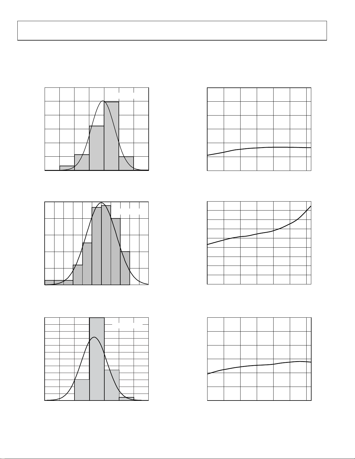
RECEIVER CHARACTERISTICS
fIN = 400 MHz, f
= 70 MHz, f
OUT
= 330 MHz, see Figure 72, Tab le 6 , and Tabl e 8.
LO
60
MEAN: 5.57dB
50
40
30
PERCENTAGE
20
10
0
5.37 5.42 5.47 5. 52 5.57 5.62 5.67 5.72
Figure 7. Gain Hi stogram; f
25
20
15
10
PERCENTAGE
5
0
19.9 20.0 20.1 20.2 20. 3 20.4 20.5 20.6 20.7 20. 8 20.9 21.0
Figure 8. Input IP3 Histogram; fIN = 400 MHz, f
CONVERSION G AIN (dB)
= 400 MHz, f
IN
INPUT IP3 (dBm)
= 70 MHz
OUT
MEAN: 20.5dBm
= 70 MHz
OUT
10
9
8
7
6
CONVERSION G AIN (dB)
5
01034-007
01034-008
4
TEMPERATURE (°C)
Figure 10. Gain Performance Over Temperature; f
f
= 70 MHz
OUT
24
23
22
21
20
19
INPUT IP3 (dBm)
18
17
16
15
TEMPERATURE (°C)
Figure 11. Input IP3 Performance Over Temperature; f
= 70 MHz
f
OUT
6040200–20–40 80
= 400 MHz,
IN
6040200–20–40 80
= 400 MHz,
IN
01034-010
01034-011
60
55
50
45
40
35
30
25
PERCENTAGE
20
15
10
5
0
3.24 3.26 3.28 3. 30 3.32 3.34 3.36 3.38
INPUT 1dB CO MPRESSIO N POINT (dBm)
Figure 9. Input 1 dB Compression Point Histogram; f
f
= 70 MHz
OUT
MEAN: 3.31dB
= 400 MHz,
IN
01034-009
Rev. B | Page 8 of 32
5.0
4.5
4.0
3.5
3.0
2.5
INPUT 1dB COMPRESSION POINT (dBm)
2.0
TEMPERATURE (°C)
6040200–20–40
01034-012
80
Figure 12. Input 1 dB Compression Point Performance Over Temperature;
f
= 400 MHz, f
IN
= 70 MHz
OUT
Page 9
AD8343
fIN = 900 MHz, f
35
= 170 MHz, fLO = 730 MHz, see Figure 72, Tabl e 6, and Tabl e 8.
OUT
6
30
25
20
15
PERCENTAGE
10
5
0
CONVERSION G AIN (dB)
Figure 13. Gain Histogram; f
30
28
26
24
22
20
18
16
14
12
PERCENTAGE
10
8
6
4
2
0
Figure 14. Input IP3 Histogram; f
30
28
26
24
22
20
18
16
14
12
PERCENTAGE
10
8
6
4
2
0
INPUT 1dB COMPRESSION POINT (d Bm)
= 900 MHz, f
IN
INPUT IP3 (dBm)
= 900 MHz, f
IN
Figure 15. Input 1 dB Compression Point Histogram; f
f
= 170 MHz
OUT
MEAN: 3.63dB
OUT
MEAN: 19.4dBm
19.619.419.219.018.818.618.418.2 20.420.220.019.8
OUT
MEAN: 3.62dBm
3.663.643.623.603.583.563.543.52 3.723.703.68
3.753.703.653.603.553.503.453.40 3.853.80
= 170 MHz
= 170 MHz
= 900 MHz,
IN
5
4
3
2
CONVERSION GAIN (dB)
1
01034-013
01034-014
01034-015
0
TEMPERATURE (°C)
Figure 16. Gain Performance Over Temperature; f
f
= 170 MHz
OUT
23
22
21
20
19
18
INPUT IP3 (dBm)
17
16
15
TEMPERATURE (°C)
Figure 17. Input IP3 Performance Over Temperature; f
f
= 170 MHz
OUT
5.0
4.5
4.0
3.5
3.0
2.5
INPUT 1dB COM PRESSION P OINT (dBm)
2.0
TEMPERATURE (°C)
6040200–20–40
= 900 MHz ,
IN
6040200–20–40 80
= 900 MHz,
IN
6040200–20–40
01034-016
80
01034-017
01034-018
80
Figure 18. Input 1dB Compression Point Performance Over Temperature;
= 900 MHz, f
f
IN
= 170 MHz
OUT
Rev. B | Page 9 of 32
Page 10
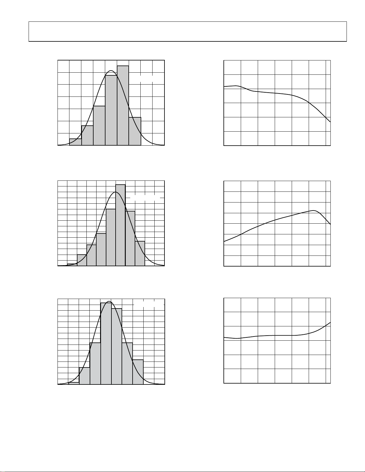
AD8343
fIN = 1900 MHz, f
28
26
24
22
20
18
16
14
12
PERCENTAGE
10
8
6
4
2
0
Figure 19. Gain Histogram; f
= 170 MHz, fLO = 1730 MHz, see Figure 72, Ta ble 6, and Table 8 .
OUT
MEAN: 7.09dB
CONVERS ION G AIN (d B)
IN
7.107.057.006.956.906.856.806.75 7.307.257.207.15
= 1900 MHz, f
= 170 MHz
OUT
01034-019
10
9
8
7
6
CONVERSION G AIN (dB)
5
4
TEMPERATURE (°C)
Figure 22. Gain Performance Over Temperature; f
= 170 MHz
f
OUT
6040200–20–40 80
= 1900 MHz,
IN
01034-022
45
40
MEAN: 16.54dBm
35
30
25
20
PERCENTAGE
15
10
5
0
INPUT IP3 (dBm)
Figure 20. Input IP3 Histogram; fIN = 1900 MHz, f
50
45
40
35
30
25
20
PERCENTAGE
15
10
5
0
INPUT 1d B COMP RESSIO N POI NT (dBm)
Figure 21. Input 1 dB Compression Point Histogram; f
f
= 170 MHz
OUT
17.517.016.516.015.515.014.514.0 18.518.0
= 170 MHz
OUT
MEAN: 2.8dBm
2.952.902.852.802.752.702.652.60 3.053.00
= 1900 MHz,
IN
18
17
16
15
14
13
INPUT IP3 (dBm)
12
11
01034-020
01034-021
10
TEMPERATURE (°C)
Figure 23. Input IP3 Performance Over Temperature; f
= 170 MHz
f
OUT
5.0
4.5
4.0
3.5
3.0
2.5
INPUT 1dB COM PRESSION P OINT (dBm)
2.0
TEMPERATURE (°C)
6040200–20–40 80
= 1900 MHz,
IN
6040200–20–40
01034-023
01034-024
80
Figure 24. Input 1 dB Compression Point Performance Over Temperature;
f
= 1900 MHz, f
IN
= 170 MHz
OUT
Rev. B | Page 10 of 32
Page 11

AD8343
fIN = 2400 MHz, f
40
35
30
25
= 170 MHz, fLO = 2230 MHz, see Figure 72, Table 6, and Table 8.
OUT
MEAN: 6.79dB
10
9
8
20
15
PERCENTAGE
10
5
0
CONVERSION GAIN (dB)
Figure 25. Gain Histogram; f
35
MEAN: 14.46dBm
30
25
20
15
PERCENTAGE
10
5
0
Figure 26. Input IP3 Histogram; f
45
40
35
30
25
20
PERCENTAGE
15
10
5
0
1.90 1.95 2.00 2.05 2.10 2.15 2.20 2.25 2.30 2.35 2.40
INPUT 1dB CO M P RE S S ION POINT (dBm)
= 2400 MHz, f
IN
INPUT IP3 (dBm)
= 2400 MHz, f
IN
Figure 27. Input 1 dB Compression Point Histogram; f
= 170 MHz
f
OUT
7.06.8 7.66.66.46.26.05.8 7.47.2
= 170 MHz
OUT
= 170 MHz
OUT
INPUT: 2. 11 dBm
= 2400 MHz,
IN
7
6
CONVERSION GAIN (dB)
5
01034-025
01034-026
15.613.0 13.2 13.4 13.6 13.8 14.0 14.2 14.4 14.6 14.8 15.0 15.2 15.4
01034-027
4
TEMPERATURE (°C)
Figure 28. Gain Performance Over Temperature; f
f
= 170 MHz
OUT
18
17
16
15
14
13
INPUT IP3 (dBm)
12
11
10
TEMPERATURE (°C)
Figure 29. Input IP3 Performance Over Temperature; f
= 170 MHz
f
OUT
3.0
2.5
2.0
1.5
1.0
0.5
INPUT 1dB CO M P RE S S ION POINT (dBm)
0
TEMPERATURE (°C)
6040200–20–40
= 2400 MHz,
IN
6040200–20–40
= 2400 MHz,
IN
6040200–20–40
01034-028
80
01034-029
80
01034-030
80
Figure 30. Input 1 dB Compression Point Performance Over Temperature;
= 2400 MHz, f
f
IN
= 170 MHz
OUT
Rev. B | Page 11 of 32
Page 12

AD8343
fIN = 2400 MHz, f
24
22
20
18
16
14
12
10
PERCENTAGE
8
6
4
2
0
Figure 31. Gain Histogram; f
22
20
18
16
14
12
10
PERCENTAGE
8
6
4
2
0
14.8
Figure 32. Input IP3 Histogram; f
65
60
55
50
45
40
35
30
25
PERCENTAGE
20
15
10
5
0
2.00 2.05 2.10 2.15 2.20 2.25 2.30 2.35 2.40 2.45 2.50
Figure 33. Input 1 dB Compression Point Histogram; f
= 425 MHz, fLO = 1975 MHz, see Figure 72, Ta ble 6, and Table 8 .
OUT
MEAN: 5.40dB
01034-031
CONVERSION G AIN (dB)
= 2400 MHz, f
IN
15.0
15.2
15.4
15.6
15.8
16.0
16.2
16.4
INPUT IP3 (dBm)
= 2400 MHz, f
IN
INPUT 1dB COMPRESSION POINT (dBm)
= 425 MHz
f
OUT
OUT
MEAN: 16.50dBm
16.6
16.8
17.0
MEAN: 2.22dBm
= 425 MHz
17.2
= 425 MHz
OUT
= 2400 MHz,
IN
6.64.2 4.4 4.6 4. 8 5.0 5.2 5. 4 5.6 5.8 6. 0 6.2 6.4
01034-032
18.0
17.8
17.6
17.4
01034-033
10
9
8
7
6
CONVERSION GAIN (dB)
5
4
TEMPERATURE ( °C)
Figure 34. Gain Performance Over Temperature; f
f
= 425 MHz
OUT
18
17
16
15
14
13
INPUT IP3 (dBm)
12
11
10
TEMPERATURE (° C)
Figure 35. Input IP3 Performance Over Temperature; f
f
= 425 MHz
OUT
3.0
2.5
2.0
1.5
1.0
0.5
INPUT 1dB COM PRESSION POINT (d Bm)
0
TEMPERATURE (° C)
6040200–20–40
= 2400 MHz,
IN
6040200–20–40
= 2400 MHz,
IN
6040200–20–40
01034-034
80
01034-035
80
01034-036
80
Figure 36. Input 1 dB Compression Point Performance Over Temperature;
f
= 2400 MHz, f
IN
= 425 MHz
OUT
Rev. B | Page 12 of 32
Page 13

AD8343
TRANSMIT CHARACTERISTICS
fIN = 150 MHz, f
35
= 900 MHz, fLO = 750 MHz, see Figure 72, Tabl e 6, and Tabl e 7.
OUT
10
18.15
MEAN: 7.49dBm
= 900 MHz
OUT
MEAN: 18.1dBm
18.20
18.25
OUT
MEAN: 1.9dBm
18.30
= 900 MHz
30
25
20
15
PERCENTAGE
10
5
0
7.20 7.25 7.30 7.35 7.40 7.50 7.557.45 7.60 7.65 7.70
Figure 37. Gain Histogram; f
24
22
20
18
16
14
12
10
PERCENTAGE
8
6
4
2
0
17.80
17.85
CONVERSION G AIN (dB)
17.90
17.95
18.00
INPUT IP3 (dBm)
= 150 MHz, f
IN
18.05
18.10
Figure 38. Input IP3 Histogram; fIN = 150 MHz, f
24
22
20
18
16
14
12
10
PERCENTAGE
8
6
4
2
0
1.55 1.60 1.65 1.70 1.75 1.85 1.901.80 1.95 2.00 2.05 2.10 2.15 2.20
INPUT 1dB COMPRESSION POINT (dBm)
Figure 39. Input 1 dB Compression Point Histogram;
= 150 MHz, f
f
IN
= 900 MHz
OUT
9
8
7
6
CONVERSION GAIN (dB)
5
01034-037
4
TEMPERATURE ( °C)
6040200–20–40
01034-040
80
Figure 40. Gain Performance Over Temperature;
= 150 MHz, f
f
IN
20
19
18
17
16
15
INPUT IP3 (dBm)
14
01034-038
18.35
18.45
18.40
13
12
Figure 41. Input IP3 Performance Over Temperature; f
f
OUT
3.0
2.5
2.0
1.5
1.0
INPUT 1dB COM PRESION (d Bm)
0.5
01034-039
0
= 900 MHz
OUT
TEMPERATURE (° C)
= 900 MHz
TEMPERATURE (° C)
6040200–20–40
= 150 MHz,
IN
6040200–20–40
01034-041
80
01034-042
80
Figure 42. Input 1dB Compression Point Performance Over Temperature;
f
= 150 MHz, f
IN
= 900 MHz
OUT
Rev. B | Page 13 of 32
Page 14

AD8343
fIN = 150 MHz, f
40
35
30
25
20
15
PERCENTAGE
10
5
0
Figure 43. Gain Histogram; f
50
45
40
35
30
25
20
PERCENTAGE
15
10
5
0
Figure 44. Input IP3 Histogram; f
45
40
35
30
25
20
PERCENTAGE
15
10
5
0
Figure 45. Input 1 dB Compression Point Histogram; f
= 1900 MHz, fLO = 1750 MHz, see Figure 72, Ta ble 6, and Tabl e 7.
OUT
MEAN: 0.25dB
CONVERSION G AIN (dB)
= 150 MHz, f
IN
INPUT IP3 (dBm)
IN
INPUT 1d B COMP RESSIO N POI NT (dBm)
f
= 1900 MHz
OUT
0.60.40.2 1.4–1.0 –0.8 –0.6 –0. 4 –0.2 0 1.21.00.8
14.514.013.5 17.010.5 11.0 11.5 12.0 12.5 13.0 16.516.015.0 15.5
= 150 MHz, f
MEAN: 0.79dBm
= 1900 MHz
OUT
MEAN: 13.4dBm
= 1900 MHz
OUT
3.02.52.0 3.5–1.0 –0.5 0 0.5 1.0 1.5
= 150 MHz,
IN
01034-043
01034-044
01034-045
Figure 48. Input 1 dB Compression Point Performance Over Temperature;
5
4
3
2
1
0
CONVERSION G AIN (dB)
–1
–2
TEMPERATURE (° C)
Figure 46. Gain Performance Over Temperature; f
= 1900 MHz
f
OUT
18
17
16
15
14
13
INPUT IP3 (dBm)
12
11
10
9
TEMPERATURE (° C)
Figure 47. Input IP3 Performance Over Temperature; f
= 1900 MHz
f
OUT
2.0
1.5
1.0
0.5
0
–0.5
INPUT 1dB COMPRESSION POINT (dBm)
–1.0
TEMPERATURE (° C)
= 150 MHz, f
f
IN
= 1900 MHz
OUT
6040200–20–40
= 150 MHz,
IN
6040200–20–40
= 150 MHz,
IN
6040200–20–40
01034-046
80
01034-047
80
01034-048
80
Rev. B | Page 14 of 32
Page 15

AD8343
CIRCUIT DESCRIPTION
The AD8343 is a mixer intended for high-intercept applications.
The signal paths are entirely differential and dc-coupled to
permit high-performance operation over a broad range of
frequencies; the block diagram (see
Figure 1) shows the basic
functional blocks. The bias cell provides a PTAT (proportional
to absolute temperature) bias to the LO driver and core. The LO
driver consists of a three-stage limiting differential amplifier
that provides a very fast (almost square-wave) drive to the bases
of the core transistors.
The AD8343 core utilizes a standard architecture where the
signal inputs are directly applied to the emitters of the transistors in the cell (see
Figure 49 and Figure 55). The bases are
driven by the hard-limited LO signal that directs the transistors
to steer the input currents into periodically alternating pairs of
output terminals, thus providing the periodic polarity reversal
that effectively multiplies the signal by a square wave of the LO
frequency.
COMM
BIAS
DRIVER
MIXER
CORE
LO
Figure 49. Topology
14118715
AD8343
Q1 Q2 Q3 Q4
2 3
INPP
INPM
13
12
OUTP
OUTM
01034-049
DCPL
PWDN
LOIP
LOIM
VPOS
4
6
10
9
To illustrate this functionality, when LOIP is positive, Q1
and Q4 are turned on, and Q2 and Q3 are turned off. In this
condition, Q1 connects I
to OUTM and Q4 connects I
INPP
INPM
to OUTP. When LOIP is negative, the roles of the transistors
reverse, steering I
to OUTP and I
INPP
to OUTM. Isolation
INPM
and gain are possible because, at any instant, the signal passes
through a common-base transistor amplifier pair.
Multiplication is the essence of frequency mixing; an ideal
multiplier would make an excellent mixer. The theory is
expressed in the following trigonometric identity:
t) × sin(ωLOt) = ½[cos(ω
sin(ω
sig
t − ωLOt) − cos(ω
sig
t + ωLOt)]
sig
This states that the product of two sine-wave signals of different
frequencies is a pair of sine waves at frequencies equal to the
sum and difference of the two frequencies being multiplied.
Unfortunately, practical implementations of analog multipliers
generally make poor mixers because of imperfect linearity and
the added noise that invariably accompanies attempts to improve
linearity. The best mixers to date are those that use the LO
signal to periodically reverse the polarity of the input signal.
In this class of mixers, frequency conversion occurs as a
result of multiplication of the signal by a square wave at the
LO frequency. Because a square wave contains odd harmonics
in addition to the fundamental, the signal is effectively multiplied by each frequency component of the LO. The output of
the mixer therefore contains signals at F
± F
5× F
LO
, 7×FLO ± F
sig
, etc. The amplitude of the components
sig
LO
± F
sig
, 3×F
LO
± F
,
sig
arising from signal multiplication by LO harmonics falls off
with increasing harmonic order because the amplitude of a
square wave’s harmonics falls off.
An example of this process is illustrated in
Figure 50. The first
pane of this figure shows an 800 MHz sinusoid intended to
represent an input signal. The second pane contains a square
wave representing an LO signal at 600 MHz which has been
hard-limited by the internal LO driver. The third pane shows
the time domain representation of the output waveform and the
fourth pane shows the frequency domain representation. The
two strongest lines in the spectrum are the sum and difference
frequencies arising from multiplication of the signal by the LOs
fundamental frequency. The weaker spectral lines are the result
of the multiplication of the signal by various harmonics of the
LO square wave.
SIGNAL
7 × LO – SI G
LOCAL
OSCILLAT OR
SIG × LO
SIG × LO
5 × LO + SIG
TIME
DOMAIN
FREQUENCY
DOMAIN
SIG – LO
Figure 50. Signal Switching Characteristics of the AD8343
3 × LO – SI G
SIG + LO
FREQUENCY
5 × LO – SI G
3 × LO + SIG
01034-050
Rev. B | Page 15 of 32
Page 16

AD8343
DC INTERFACES
BIASING AND DECOUPLING (VPOS, DCPL)
VPOS is the power supply connection for the internal bias circuit
and the LO driver. Bypass this pin closely to GND with a
capacitor in the range of 0.01 µF to 0.1 µF. The DCPL pin
provides access to an internal bias node for noise bypassing
purposes. Bypass this node to COMM with 0.1 µF.
POWER-DOWN INTERFACE (PWDN)
The AD8343 is active when the PWDN pin is held low; otherwise the device enters a low-power state as shown in
45
40
35
30
25
20
15
DEVICE CURRENT (mA)
10
5
0
POWER-DOW N VOLTAG E (V)
POWER-DOW N
SWEPT FROM
BOTH 3V TO 5V
AND 5V TO 3V
Figure 51. Device Current vs. PWDN Voltage
To assure full power-down, the PWDN voltage must be within
0.5 V of the supply voltage at VPOS. Normal operation requires
that the PWDN pin be taken at least 1.5 V below the supply
voltage. The PWDN pin sources about 160 µA when pulled to
GND (see the
Pin Configuration and Function Descriptions
section). It is not advised to leave the pin floating when the
device is disabled; a resistive pull-up to VPOS is the minimum
suggestion.
The AD8343 requires about 2.2 µs to turn off when PWDN is
asserted; turn-on time is about 500 ns.
Figure 52 and Figure 53
show typical characteristics (they vary with bypass component
values).
Figure 54 shows the test configuration used to acquire
these waveforms.
Figure 51.
4.54.03.53.0 5.0
01034-051
1
2
CH1 200nVΩ CH2 1.00VΩ M500ns CH2 4.48V
Figure 52. PWDN Response Time Device On to Off
1
2
CH1 200nVΩ CH2 1.00VΩ M100ns CH2 4.48V
Figure 53. PWDN Response Time Device Off to On
TEKTRONIX
TDS694C
OSCILLOSCOPE
AD8343
1
COMM
COMM
2
INPP
3
INPM
OUTM
4
DCPL
COMM
5
VPOS
6
PWDN
7
COMM
COMM
OUTP
LOIP
LOIM
14
13
12
11
10
9
8
HP8648C
SIGNAL
GENERATOR
MATCHING
NETWORK AND
TRANSFORMER
1nH
VPOS
HP8130
PULSE
GENERATOR
TRIGGER
RF INPUT
1740MHz
0.1µF
0.1µF
Figure 54. PWDN Response Time Test Schematic
IF OUTPUT
170MHz
MATCHING
NETWORK AND
TRANSFORMER
TRANSFORMER
HP8648C
SIGNAL
GENERATOR
01034-052
01034-053
LO INPUT
1570MHz
01034-054
Rev. B | Page 16 of 32
Page 17

AD8343
AC INTERFACES
Because of the AD8343’s wideband design, there are several
points to consider in its ac implementation; the basic ac signal
connection diagram shown in
points. The input signal undergoes a single-ended to differential
conversion and is then reactively matched to the impedance
presented by the emitters of the core. The matching network
also provides bias currents to these emitters. Similarly, the LO
input undergoes a single-ended-to-differential transformation
before it is applied to the 50 Ω differential LO port. The differential
output signal currents appear at open-collectors and are reactively matched and converted to a single-ended signal.
Figure 55 summarizes these
VPOS
DCPL
4
PWDN
6
LOIP
10
LOIM
9
SINGLE-ENDED-TO-DIFFERENTIAL
CONVERSION
SINGLE-E NDED
LO INPUT SIGNAL
Figure 55. Basic AC Signal Connection Diagram
DIFFERENTIAL-TO -SINGLE -ENDED
COMM
BIAS
CELL
LO
DRIVER
INPUT MATCHING
CORE BIAS NETW ORK
SINGLE-E NDED-TO-DIFFERENTI AL
SINGLE-E NDED
INPUT SIGNAL
CONVERSION
OUTPUT MAT CHING NETW ORK
CORE BIAS NETW ORK
14118715
AD8343
INPP
2 3
NETWORK
CONVERSION
INPM
SINGLE- ENDED
OUTPUT SI GNAL
OUTP
13
OUTM
12
CORE
01034-055
Rev. B | Page 17 of 32
Page 18

AD8343
()(
(
INPUT INTERFACE (INPP AND INPM)
SINGLE-ENDED-TO-DIFFERENTIAL CONVERSION
The AD8343 is designed to accept differential input signals for
best performance. While a single-ended input can be applied,
the signal capacity is reduced by 6 dB. Furthermore, there is no
cancellation of even-order distortion arising from the nonlinear
input impedances, so the effective signal handling capacity is
reduced even further in distortion-sensitive situations. That is,
the intermodulation intercepts are degraded.
For these reasons, it is strongly recommended that differ
ential signals be presented to the AD8343’s input. In addition
to commercially available baluns, there are various discrete and
printed circuit networks that can produce the required balanced
waveforms and impedance match. These alternate circuits can
be employed to possibly reduce the component cost of the
mixer and/or improve performance.
Baluns implemented in transmission line form (also known as
common-mode chokes) are useful up to frequencies of around
1 GHz to 2 GHz, but are often excessively lossy at the higher
frequencies that the AD8343 can handle. M/A-COM manufactures these baluns and Murata produces a true surface-mount
balun. Coilcraft® and Toko are also manufacturers of RF baluns.
INPUT MATCHING CONSIDERATIONS
The design of the input matching network must be undertaken
with two goals in mind: matching the source impedance to the
input impedance of the AD8343 and providing a dc bias current
path for the bias setting resistors.
The maximum power transfer into the device occurs when
there is a conjugate impedance match between the signal source
and the input of the AD8343. This match is achieved with the
differential equivalent of the classic L network, as illustrated in
Figure 56. The figure gives two examples of the transformation
from a single-ended L network to its differential counterpart.
The design of L matching networks is adequately covered in
texts on RF amplifier design (for example, Microwave Transistor
Amplifiers by Guillermo Gonzalez).
L1
C1
C2
L2
SINGL E-ENDE D DI FFE RENTI AL
Figure 56. Single-Ended-to-Differential Transformation
Figure 57 shows the differential input impedance of the
AD8343 at the pins of the device. The two measurements
shown in the figure are for two different core currents set by
Resistor R3 and Resistor R4; the real value impedance shift is
L1/2
L1/2
C1
2C2
L2
2C2
01034-056
caused by the change in Transistor r
current. The standard S parameter files are available through
Analog Devices.
68Ω
Figure 57. Input Differential Impedance (INPP, INPM) for Two Values of
134Ω
2500MHz
1500MHz
1000MHz
500MHz
50MHz
FREQUENCY (50MHz TO 2500MHz)
R3 and R4
Figure 57 provides a reasonable starting point for the design
of the network. However, the particular board traces and pads
transform the input impedance at frequencies in excess of about
500 MHz. For this reason, it is best to make a differential input
impedance measurement at the board location where the matching
network is installed, as a starting point for designing an
accurate matching network.
Differential impedance measurement is made relatively easy
using a technique presented in an article by Lutz Konstroffer in
RF Design, Vol. 22, January 1999, Page 24, 28; entitled “Finding
the Reflection Coefficient of a Differential One-Port Device.”
This article presents a mathematical formula for converting
from a two-port single ended measurement to differential
impedance. A full two-port measurement is performed using a
vector network analyzer with Port 1 and Port 2 connected to the
two differential inputs of the device at the desired measurement
plane. The two-port measurement results are then processed
with Konstroffer’s formula. This formula is straightforward and
can be implemented through most RF design packages that can
read and analyze network analyzer data. The Konstroffer
formula is:
s
=Γ
()( )( )()
This measurement can also be made using two ports of a
4-port vector network analyzer. This instrument, and
accompanying software, is capable of directly producing
differential measurements.
At low frequencies and I
= 16 mA, the differential input
O
impedance seen at ports INPP and INPM of the AD8343 is
low (~5 Ω in series with parasitic inductances that total about
3 nH). Because of this low value of impedance, it is beneficial
to choose a transformer-type balun that can also perform all or
part of the real value impedance transformation. The turns ratio
of the transformer removes some of the matching burden from
the differential L-network and should help lead to wider
due to the change in
e
)( )
01034-057
)
S12S22S21S11S12S22S21S11
×−+−−+−−−×
21112
S22S21S11S12S22S21
+−−+−−−
1112
Rev. B | Page 18 of 32
Page 19

AD8343
bandwidth matches. At frequencies above 1 GHz, the real part
of the input impedance rises markedly and it becomes more
attractive to use a 1:1 balun and rely on the L network for the
entire impedance transformation.
In order to obtain the lowest distortion, the inputs of the AD8343
are driven through external ballast resistors. At low frequencies
(up to perhaps 200 MHz), about 5 Ω per side is appropriate;
above about 400 MHz, 10 Ω per side is better. The specified
RF performance values for the AD8343 apply with these ballast
resistors in use. These resistors improve linearity because their
linear ac voltage drop partially swamps the nonlinear voltage
swing occurring on the emitters.
In cases where the use of a lossy balun is unavoidable, it can be
worthwhile to perform simultaneous matching on both the
input and output sides of the balun. The idea is to independently
characterize the balun as a two-port device and then arrange a
simultaneous conjugate match for it. Unfortunately, there seems
to be no good way to determine the benefit this approach offers
in any particular case; it remains necessary to characterize the
balun and then design and simulate appropriate matching networks to make an optimal decision. One indication that such
effort is worthwhile is the discovery that the adjustment of a
post-balun-only matching network for best gain differs appreciably from that which produces best return loss at the baluns
input. A better tactic is to try a different approach for the balun,
either purchasing a different balun or designing a discrete
network, for lower loss.
For more information on performing the input match, see
the section entitled A Step-by-Step Approach to Impedance
Matching.
INPUT BIASING CONSIDERATIONS
The mixer core bias current of the AD8343 is adjustable from
less than 5 mA to a safe maximum of 20 mA. It is important to
note that the reliability of the AD8343 can be compromised for
core currents set to higher than 20 mA. The AD8343 is tested to
ensure that a value of 68.1 Ω ±1% ensures safe operation.
Higher operating currents reduce distortion and affect gain,
noise figure, and input impedance (Figure 58 and Figure 59).
As the quiescent current is increased by a factor of N, the real
part of the input impedance decreases by N. Assuming that a
match is maintained, the signal current increases by √N, but the
signal voltage decreases by √N, exercising a smaller portion of
the nonlinear V–I characteristic of the common base connected
mixer core transistors and results in lower distortion.
At low frequencies where the magnitude of the complex input
impedance is much smaller than the bias resistor values, adequate biasing can be achieved simply by connecting a resistor
from each input to GND. The input terminals are internally
biased at 1.2 V dc (nominal), so each resistor has a resistance
value calculated as R
well matched in order to maintain full LO to output isolation;
1% tolerance resistors are recommended.
20
16
12
8
TOTAL SUPPLY CURRENT
4
CONVERSION G AIN AND NOISE F IGURE (d B)
0
20 40 60 80 100 120 140 160 180 200
Figure 58. Effect of R3 and R4 Value on Gain and Noise Figure
25
20
15
10
5
INPUT IP3 (dBm) AND P1dB (dBm)
0
20 40 60 80 100 120 140 160 180 200
Figure 59. Effect of R3 and R4 Value on Input IP3 and Gain Compression
At higher frequencies where the input impedance of the AD8343
rises, it is beneficial to insert an inductor in series between each
bias resistor and the corresponding input pin in order to minimize signal shunting (Figure 72). Practical considerations limit
the inductive reactance to a few hundred ohms. The best overall
choice of inductor is the value that places the self-resonant
frequency at about the upper end of the desired input frequency
range. Note that there is an RF stability concern that argues in
favor of erring on the side of too small an inductor value; see
the Input and Output Stability Considerations section. The
Murata LQW1608A series of inductors (0603 SMT package)
offers values up to 56 nH before the self-resonant frequency
falls below 2.4 GHz.
For optimal LO-to-output isolation, it is important not to
connect the dc nodes of the emitter bias inductors together
in an attempt to share a single bias resistor. Doing so causes
isolation degradation arising from V
transistors in the core.
= 1.2/I
BIAS
INPUT IP3
TOTAL SUPPLY CURRENT
. The resistor values should be
BIAS
INPUT RF = 900MHz
OUTPUT I F = 170MHz
LO LOW SIDE INJECTION
GAIN
R3 AND R4 (Ω)
INPUT RF = 900MHz
OUTPUT I F = 170MHz
LO LOW SIDE INJECTION
P1dB
R3 AND R4 (Ω)
NOISE FI GURE
mismatches of the
BE
90
80
70
60
50
40
30
20
10
0
100
90
80
70
60
50
40
30
20
10
0
TOTAL SUPPLY CURRENT (mA)
01034-058
TOTAL SUPPLY CURRENT (mA)
01034-059
Rev. B | Page 19 of 32
Page 20

AD8343
OUTPUT INTERFACE (OUTP, OUTM)
The output of the AD8343 comprises a balanced pair of open
collector outputs. These should be biased to about the same
voltage as is connected to VPOS. Connecting them to an appreciably higher voltage is likely to result in conduction of the ESD
protection network on signal peaks, causing high distortion levels.
On the other hand, setting the dc level of the outputs too low is
also likely to result in poor device linearity due to collector-base
capacitance modulation or saturation of the mixer core transistors.
OUTPUT MATCHING CONSIDERATIONS
The AD8343 requires a differential load for much the same
reasons that the input needs a differential source to achieve
optimal device performance. In addition, a differential load
provides the best LO to output isolation and the best input to
output isolation.
At low output frequencies, it is usually not appropriate to
arrange a conjugate match between the device output and
the load, even though doing so maximizes the small signal
conversion gain. This is because the output impedance at low
frequencies is quite high (a high resistance in parallel with a
small capacitance). See
output impedance measured at the device pins. This data is
available in standard file format at the Analog Devices website
(
http://www.analog.com); search for AD8343, then click on
AD8343 S-Parameters. If a matching high impedance load is
used, sufficient output voltage swing occurs to cause output
clipping even at relatively low input levels, constituting a loss
of dynamic range. The linear range of voltage swing at each
output pin is about ±1 V from the supply voltage VPOS. A
good compromise is to provide a load impedance of about
200 to 500 Ω between the output pins at the desired output
frequency (based on 15 mA to 20 mA bias current at each
input). At output frequencies below 500 MHz, more output
power can be obtained before the onset of gross clipping by
using a lower load impedance; however, both gain and low
order distortion performance can be degraded.
Figure 60. Output Differential Impedance (OUTP, OUTM)
Figure 60 for a plot of the differential
FREQUENCY (50MHz TO 2500MHz )
50MHz
2000MHz
1500MHz
500MHz
1000MHz
01034-060
The output load impedance must also be kept reasonably low
at the image frequency to avoid developing appreciable extra
voltage swing, which can reduce dynamic range.
If maintaining a good output return loss is not required, a 4:1 to
8:1 (impedance) flux-coupled transformer can be used to present a
suitable load to the device and to provide collector bias via a
center tap as shown in
Figure 69. At all but the lowest output
frequencies, it becomes desirable to tune out the output capacitance of the AD8343 by connecting an inductor between the
output pins. On the other hand, when a good output return loss
is desired, the output can be resistively loaded with a shunt
resistance between the output pins in order to set the real value
of output impedance. With selection of both the transformer’s
impedance ratio and the shunting resistance as required, the
desired total load (~500 Ω) is achieved while optimizing both
signal transfer and output return loss.
At higher output frequencies, the output conductance of the
device becomes higher (see
Figure 60), with the consequence
that above about 900 MHz, it does become appropriate to
perform a conjugate match between the load and the AD8343s
output. The device’s own output admittance becomes sufficient
to remove the threat of clipping from excessive voltage swing.
Just as for the input, it is best to perform differential output
impedance measurements on the board layout to effectively
develop a good matching network.
OUTPUT BIASING CONSIDERATIONS
When the output single-ended-to-differential conversion takes
the form of a transformer whose primary winding is center
tapped, simply apply VPOS to the tap, preferably through a
ferrite bead in series with the tap in order to avoid a common
mode instability problem (see the
Considerations
section). See Figure 69 for an example of this
network. The collector dc bias voltage must be nominally equal
to the supply voltage applied to Pin 5 (VPOS).
If a 1:1 transmission line balun is used for the output, it is
necessary to bring in collector bias through separate inductors.
These inductors are chosen to obtain a high impedance over
the RF output frequency range of interest. See
example of this network.
Input and Output Stability
Figure 70 for an
Rev. B | Page 20 of 32
Page 21

AD8343
V
INPUT AND OUTPUT STABILITY CONSIDERATIONS
The differential configuration of the input and output ports of
the AD8343 raises the need to consider both differential and
common-mode RF stability of the device. Throughout the
following stability discussion, common mode is used to refer to
a signal that is referenced to ground. The equivalent commonmode impedance is the value of impedance seen from the node
under discussion to ground. The book, Microwave Transistor
Amplifiers by Guillermo Gonzalez, also has an excellent section
covering stability of amplifiers.
The AD8343 is unconditionally stable for any differential
impedance, so device stability need not be considered with
respect to the differential terminations. However, the device is
potentially unstable (k factor is less than one) for some commonmode impedances.
output common-mode stability regions, respectively.
Figure 61 and Figure 62 plot the input and
Figure 63
shows the test equipment configuration to measure these
stability circles.
The plotted stability circles in
Figure 62 indicate that the guiding
principle for preventing stability problems due to commonmode output loading is to avoid high-Q common-mode inductive
loading. This stability concern is of particular importance when
the output is taken from the device with a center-tapped transformer. The common-mode inductance to the center tap arises
from imperfect coupling between the halves of the primary
winding and produces an unstable common-mode loading
condition. Fortunately, a simple solution is to insert a ferrite
bead in series with the center tap, then provide effective RF
bypassing on the power supply side of the bead. The bead
develops substantial impedance (tens of ohms) by the time
a frequency of about 200 MHz is reached. The Murata
BLM21P300S is a possible choice for many applications.
50MHz
150MHz
FREQUENCY: 50MHz TO 2500MHz INCREMENT: 100MHz
Figure 62. Common-Mode Output Stability Circles
4-PORT NET WORK ANALYZER
S PARAMETER TEST SET
BIAS
BIAS
BIAS
TEE
TEE
TEE
BIAS
TEE
AD8343
COMM
COMM
OUTP
OUTM
COMM
LOIP
LOIM
COMM
14
13
12
11
10
9
8
POS
1nH
0.1µF
0.1µF
1
2
3
4
5
6
7
INPP
INPM
DCPL
VPOS
PWDN
COMM
Figure 63. Impedance and Stability Circle Test Schematic
In cases where a transmission line balun is used at the output,
the solution deserves a bit more exploration. After the differential impedance matching network is designed, it is possible
to measure or simulate the common-mode impedance seen by
the device. This impedance is plotted against the stability circles
to ensure stable operation. An alternate topology for the matching
network is required if the proposed network produces an
unacceptable common-mode impedance.
150MHz
50MHz
01034-063
01034-062
FREQUENCY: 50MHz TO 2500MHz
INCREMENT: 100MHz
01034-061
Figure 61. Common-Mode Input Stability Circles
Rev. B | Page 21 of 32
Page 22

AD8343
For the device input, capacitive common-mode loading tends to
produce an unstable circuit, particularly at low frequencies (see
Figure 61). Fortunately, either type of single-ended-to-differential
conversion (transmission line balun or flux-coupled transformer)
tends to produce inductive loading, although some matching
network topologies and/or component values circumvent this
desirable behavior. In general, a simulation of the commonmode termination seen by the AD8343’s input port is plotted
against the input stability circles to check stability. This is
especially recommended if the single-ended-to-differential
conversion is done with a discrete component circuit.
LOCAL OSCILLATOR INPUT INTERFACE (LOIP, LOIM)
The LO terminals of the AD8343 are internally biased;
connections to these terminals should include dc blocks,
except as noted below in the
The differential LO input return loss (with a 50 Ω differential
input impedance) is presented in
has a typical differential return loss of better than 9.5 dB (2:1 V
SWR). If better return loss is desired for this port, differential
matching techniques can also be applied.
0
–5
–10
–15
–20
DC Coupling the LO section.
Figure 64. As shown, this port
5
4
3
2
CONVERSION G AIN (dB)
1
0
–40 –30 –20 –10
LO POW ER (dBm)
INPUT RF = 900MHz
OUTPUT IF = 170MHz
LO LOW SIDE INJECTION
CONVERSION G AIN
NOISE FI GURE
25
20
15
10
NOISE FIGURE (dB)
5
0
01034-065
Figure 65. Gain and Noise Figure vs. LO Input Power
DC COUPLING THE LO
The AD8343’s LO limiting amplifier chain is internally
dc-coupled. In some applications or experimental situations,
it is useful to exploit this property. Following is the recommended way to do so.
The LO pins are internally biased at about 360 mV with respect
to COMM. Driving the LO to either extreme requires injecting
several hundred microamps into one LO pin and extracting
about the same amount of current from the other. The incremental impedance at each pin is about 25 Ω, so the voltage level
on each pin is disturbed very little by the application of external
currents in that range.
Figure 66 illustrates how to drive the LO port with continuous
dc and also from standard ECL powered by –5.2 V.
REFLECTION COEFFICIENT (dB)
–25
–30
0 500 1000 1500 2000 2500
FREQUENCY (50MHz TO 2500MHz )
01034-064
Figure 64. LO Input Differential Reflection Coefficient
At low LO frequencies, it is reasonable to drive the AD8343
with a single-ended LO, connecting the undriven LO pin to
GND through a dc block. This results in an LO input impedance closer to 25 Ω at low frequencies, which should be factored
into the design. At higher LO frequencies, differential drive is
strongly recommended.
The suggested minimum LO power level is about –12 dBm.
This can be seen in
Figure 65.
Rev. B | Page 22 of 32
ECL
–5.2V
–5.2V
–5.2V
VPOS
DCPL
4
3.6kΩ
390Ω
1.2kΩ
390Ω
13kΩ
1kΩ
1.2kΩ
6
10
9
+5V
3.6kΩ
4
6
10
9
PWDN
LOIP
LOIM
VPOS
DCPL
PWDN
LOIP
LOIM
BIAS
LO
DRIVER
BIAS
LO
DRIVER
Figure 66. DC Interfaces to the LO Port
COMM
ECL CONTINUOUS DC
14118715
COMM
2 3
14118715
2 3
INPP
INPP
AD8343
INPM
AD8343
INPM
13
12
OUTP
13
12
OUTM
OUTPOUTM
01034-066
Page 23

AD8343
A STEP-BY-STEP APPROACH TO IMPEDANCE MATCHING
The following discussion addresses, in detail, the matter of
establishing a differential impedance match to the AD8343.
This section specifically deals with the input match, and the
use of Side A of the evaluation board (
procedure is used to establish a match to the output if desired.
Circuit Setup
The AD8343 must be powered up, driven with LO; its outputs
are terminated in a manner that avoids the common-mode
stability problem, as discussed in the
Considerations
output termination is to place ferrite chokes at L3A and L4A
and omit the output matching components altogether.
It is also important to establish the means of providing bias
currents to the input pins because this network can have
unexpected loading effects and inhibit matching progress.
section. A convenient way to deal with the
Establish Target Impedance
This step is necessary when the single-ended-to-differential
network (input balun) does not produce a 50 Ω output impedance. In order to provide for maximum power transfer, the
input impedance of the matching network, loaded with the
AD8343 input impedance (including ballast resistors), is the
conjugate of the output impedance of the single-ended-todifferential network. This step is of particular importance
when utilizing transmission line baluns because the differential
output impedance of the input balun can differ significantly
from what is expected. Therefore, it is a good idea to make a
separate measurement of this impedance at the desired operating
frequency before proceeding with the matching of the AD8343.
The idea is to make a differential measurement at the output of
the balun, with the single-ended port of the balun terminated
in 50 Ω. Again, there are two methods available for making this
measurement: use of the ATN multiport network analyzer to
measure the differential impedance directly, or use of a standard
two-port network analyzer and Konstroffer’s transformation
equation.
In order to utilize a standard two-port analyzer, connect the
two ports of the calibrated vector network analyzer (VNA) to
the balanced output pins of the balun, measure the two-port S
parameters, then use Konstroffer’s formula to convert the twoport parameters to one-port differential Γ:
()( )()(
=
Γs
()( )( )()
Figure 71). An analogous
Input and Output Stability
×−+−−+−−−×
21112
1112
S22S21S11S12S22S21
+−−+−−−
S12S22S21S11S12S22S21S11
Measure AD8343 Differential Impedance at Location of First Matching Component
Once the target impedance is established, the next step in matching
to the AD8343 is to measure the differential impedance at the
location of the first matching component. The A side of the
evaluation board is designed to facilitate doing so.
Before doing the board measurements, it is necessary to perform
a full two-port calibration of the VNA at the ends of the cables
that are used to connect to the board’s input connectors, using
the SOLT (Short, Open, Load, Thru) method or equivalent. It
is a good idea to set the VNAs sweep span to a few hundred
megahertz or more for this work because it is often useful to see
what the circuit is doing over a large range of frequencies, not
just at the intended operating frequency. This is particularly
useful for detecting stability problems.
After the calibration is complete, connect Network Analyzer
Port 1 and Network Analyzer Port 2 to the differential inputs
of the AD8343 Evaluation Board.
On the AD8343 evaluation board, it is necessary to temporarily
install jumpers at Z1A and Z3A if Z4A is the desired component
location. 0 resistors or capacitors of sufficient value to exhibit
negligible reactance work nicely for this purpose.
Next, extend the reference plane to the location of your first
matching component. This is accomplished by solidly shorting
both pads at the component location to GND Power to the
board must be off for this operation. Adjust the VNA reference
plane extensions to make the entire trace collapse to a point (or
best approximation thereof near the desired frequency) at the
zero impedance point of the Smith Chart. Do this for each port.
A reasonable way to provide a good RF short is to solder a piece
of thin copper or brass sheet on edge across the pads to the
nearby GND pads.
Now, remove the short, apply power to the board, and take
readings. Look at both S11 and S22 to verify that they remain
inside the unit circle of the Smith Chart over the whole frequency
range being swept. If they fail to do so, this is a sign that the
device is unstable (perhaps due to an inappropriate commonmode load) or that the network analyzer calibration is wrong.
Either way, the problem must be addressed before proceeding
further.
Assuming that the values look reasonable, use Konstroffer’s
formula to convert to differential Γ.
Design the Matching Network
)
Perform a trial design of a matching network utilizing standard
impedance matching techniques. The network can be designed
using single-ended network values, and then converted to
differential form as illustrated in
theoretical design of a Series C/Shun
between 50 Ω and a typical load at 1.8 GHz.
Figure 56. Figure 67 shows a
t C L-network applied
Rev. B | Page 23 of 32
Page 24

AD8343
1
2.9pF SHUNT CAPACITOR
2
1.0 2.00.50.2
Figure 67. Theoretical Design of Matching Network
5.0
This theoretical design is important because it establishes the
basic topology and the initial matching value for the network.
The theoretical value of 2.9 pF for the initial matching component is not available in standard capacitor values, so a 3.0 pF is
placed in the first shunt-matching location. This value can
prove to be too large, causing an overshoot of the 50 Ω real
impedance circle, or too small, causing the opposite effect.
Always keep in mind that this is a measure of differential
impedance. The value of the capacitor must be modified to
achieve the desired 50 Ω real impedance.
However, it occasionally happens that the inserted shunt
capacitor moves the impedance in completely unexpected
and undesired ways. This is almost always an indication that
the reference plane was improperly extended for the measurement. Readjust the reference planes and attempt the shunt
capacitor match with another calculated value.
When a differential impedance of 50 Ω (real part) is achieved,
the board must be powered down and then another short is
placed on the board in preparation for resetting the port extensions to a new reference plane location. Place this short where
the next series components are expected to be added, and it is
important that both Port 1 and Port 2 be extended to this point
on the board.
Another differential measurement must be taken at this point
to establish the starting impedance value for the next matching
component. Note that if 50 Ω PCB traces of finite length are
used to connect pads, the impedance experiences an angular
rotation to another location on the Smith Chart as indicated in
Figure 68.
1.0
0.5
3.3pF SHUNT CAPACITOR
0.2
0.2 0.5 1.0
01034-067
Figure 68. Effect of 50 Ω PCB Trace on 50 Ω Real Impedance Load
FREQUENCY = 1. 8GHz
5mm 50Ω TRACE
2.0 5.0
0
2.0
5.0
01034-068
With the reference plane extended to the location of the series
matching components, it is now necessary to readjust the shunt
capacitance value to achieve the desired 50 Ω real impedance.
However, this rotation is not very noticeable if the board traces
are fairly short or the application frequency is low.
As before, calculate the series capacitance value required to
move in the direction shown as step two in
Figure 67. Choose
the nearest standard component remembering to perform the
differential conversion, and install on the board. Again, if any
unexpected impedance transformations occur the reference
planes were probably extended incorrectly making it necessary
to readjust these planes.
This value of series capacitance adjusts to obtain the desired
value of differential impedance.
These steps apply to any of the previously discussed matching
topologies suitable for the AD8343. Also, if a target impedance
other than 50 Ω is required, simply calculate and adjust the
components to obtain the desired load impedance.
If the matching network topology requires a differential shunt
inductor between the inputs, it is necessary to place a series
blocking capacitor of low reactance in series with the inductor
to avoid creating a low resistance dc path between the input
terminals of the AD8343. Failure to heed this warning results
in very poor LO-output isolation.
Transfer the Matching Network to the Final Design
On the B side of the AD8343 evaluation board, install the matching
network and the input balun. Install the same output network as
used for the work on the A side, then power up the board and
measure the input return
loss at the RF input connector on the
board. Strictly speaking, the above procedure (if carried out
accurately) for matching the AD8343 obtains the best conversion gain. This differs materially from the condition that results
in best return loss at the board’s input if the balun is lossy.
Rev. B | Page 24 of 32
Page 25

AD8343
If the result is not as expected, the balun is probably producing
an unexpected impedance transformation. If the performance
is extremely far from the desired result and it was assumed that
the output impedance of the balun was 50 Ω, it is necessary to
measure the output impedance of the balun in question. The
design process must be repeated using the baluns output impedance instead of 50 Ω as the target. However, if the performance
is close to the desired result it is possible to tweak the values of
the matching network to achieve a satisfactory outcome.
These changes begin with a change from one standard value to
the adjacent standard value. With these minor modifications to
the matching network, one is able to evaluate the trend required
to reach the desired result.
If the result is unsatisfactory and an acceptable compromise
cannot be reached by further adjustment of the matching network, there are two options: obtain a better balun, or attempt a
simultaneous conjugate match to both ports of the balun.
Accomplishing the latter (or even evaluating the prospects for
useful improvement) requires obtaining full two-port, singleended-to-differential S parameters for the balun, and requires
the use of the ATN 4000 or a similar multiport network
analyzer test set. Gonzalez presents formulas for calculating
the simultaneous conjugate match in his book, Microwave
Transistor Amplifiers.
At higher frequencies, the measurement process described above
becomes increasingly corrupted by unaccounted for impedance
transformations occurring in the traces and pads between the
input connectors and the extended reference plane. One approach
to dealing with this problem is to access the desired measurement points by soldering down semirigid coaxial cables that
have been connected to the VNA and directly calibrated at the
free ends.
Rev. B | Page 25 of 32
Page 26

AD8343
V
V
APPLICATIONS
DOWNCONVERTING MIXER
A typical downconversion application is shown in Figure 69
with the AD8343 connected as a receive mixer. The input
single-ended-to-differential conversion is obtained through
the use of a 1:1 transmission line balun. The input matching
network is positioned between the balun and the input pins,
while the output is taken directly from a 4:1 impedance ratio
(2:1 turns ratio) transformer. The local oscillator signal at a level
of –12 dBm to –3 dBm is brought in through a second 1:1 balun.
POS
4.71Ω
LO IN
–10dBm
VPOS
0.1µF
DCPL
4
6
1:1
10
9
PWDN
LOIP
LOIM
BIAS
R1
68Ω
˜
R
FIN
COMM
A
1:1
L1
A
Z2
14118715
AD8343
INPP
2 3
Z1
A
Z2
B
INPM
L1
B
R1
68Ω
˜
V
POS
OUTPOUTM
4:1
13
FB
12
FERRITE BEAD
B
IF
OUT
Figure 69. Typical Downconversion Application
R1A and R1B set the core bias current of 18.5 mA per side. L1A
and L1B provide the RF choking required to avoid shunting the
signal. Z1, Z2A, and Z2B comprise a typical input matching
network that is designed to match the AD8343s differential
input impedance to the differential output impedance of the
balun.
The IF output is taken through a 4:1 (impedance ratio) transformer that reflects a 200 Ω differential load to the collectors.
This output coupling arrangement is reasonably broadband,
although in some cases the user might want to consider adding
a resonator tank circuit between the collectors to provide a
measure of IF selectivity. The ferrite bead (FB), in series with
the output transformer’s center tap, addresses the commonmode stability concern.
In this circuit, the PWDN pin is shown connected to GND,
enabling the mixer. In order to enter power-down mode and
conserve power, the PWDN pin must be taken within 500 mV
of VPOS. The DCPL pin is bypassed to GND with about 0.1 μF.
Failure to do so results in a higher noise level at the output of
the device.
UPCONVERTING MIXER
A typical upconversion application is shown in Figure 70. Both
the input and output single-ended-to-differential conversions
01034-069
are obtained through the use of 1:1 transmission line baluns.
The differential input and output matching networks are
designed between the balun and the I/O pins of the AD8343.
The local oscillator signal at a level of –12 dBm to –3 dBm is
brought in through a third 1:1 balun.
R1A and R1B set the core bias current of 18 mA per side. Z1,
Z2A, and Z2B comprise a typical input matching network
designed to match the AD8343s differential input impedance
to the differential output impedance of the balun. It is assumed
for this example that the input frequency is low and that the
magnitude of the device’s input impedance is therefore much
smaller than the bias resistor values, allowing the input bias
inductors to be eliminated with very little penalty in gain or
noise performance.
In this example, the output signal is taken via a differential
matching network comprising Z3 and Z4A/Z4B, then
through the 1:1 balun and dc blocking capacitors to the
single-ended output.
The output frequency is assumed to be high enough that
conjugate matching to the output of the AD8343 is desirable,
so the goal of the matching network is to provide a conjugate
match between the device’s output and the differential input of
the output balun.
This circuit uses shunt feed to provide collector bias for the
transistors because the output balun in this circuit has no
convenient center-tap. The ferrite beads, in series with the
output’s bias inductors, provide some small degree of damping
to ease the common-mode stability problem. Unfortunately, this
type of output balun can present a common-mode load that
enters the region of output instability, so most of the burden of
avoiding overt instability falls on the input circuit, presenting an
inductive common-mode termination over as broad a band of
frequencies as possible.
The PWDN pin is shown as tied to GND, enabling the mixer.
The DCPL pin must be bypassed to GND with about 0.1 μF to
bypass noise from the internal bias circuit.
POS
LO IN
0.1µF
VPOS
0.1µF
DCPL
4
BIAS
PWDN
6
0.1µF
LOIP
10
LOIM
9
0.1µF
R
FIN
LO
DRIVER
Z1
COMM
Z2
Z2
A
B
14118715
INPP
2 3
R1
A
AD8343
INPM
R1
Figure 70. Typical Upconversion Application
V
POS
FB
OUTPOUTM
Z4
13
A
Z3
Z4
12
B
FB
V
POS
B
RF
OUT
01034-070
Rev. B | Page 26 of 32
Page 27

AD8343
EVALUATION BOARD
The AD8343 evaluation board has two independent areas,
denoted A and B. The circuit schematics are shown in Figure 71
and Figure 72. An assembly drawing is included in Figure 73 to
ease identification of components, and representations of the
board layout are included in Figure 74 through Figure 77.
The A region is configured for ease in making device impedance measurements as part of the process of developing suitable
matching networks for a final application. The B region is designed
for operating the AD8343 in a single-ended application environment and therefore includes pads for attaching baluns or
transformers at both the input and output.
Table 6. Values of Support Components Shipped with Evaluation Board and Used for Device Characterization
Component Designator Value Quantity Manufacturer/Part Number
C1A, C1B, C3A, C3B, C11A, C11B 0.1 μF 6 Murata
C2A, C2B, C4A, C4B, C5A, C5B, C6A, C6B, C9A, 0.01 μF 16 Murata
C9B, C10A, C10B, C12A, C12B, C13A, C13B
R3A, R3B, R4A, R4B 68.1 Ω ± 1% 4 Panasonic
R1A, R1B, R2A, R2B 3.9 Ω ± 5% 4 Panasonic
R5A, R5B 0 Ω 2 Panasonic
J1A, J1B Ferrite Bead 2 Murata
T1A, T1B, T2B (Various) 1:1 3 M/A-COM ETC1-1-13 Wideband Balun
T3B (Various) 4:1 1 Mini-Circuits® TC4-1W Transformer
R6A, R6B, R7A, R7B 10 Ω ± 1% 4 Panasonic
L1A, L1B, L2A, L2B 56 nH 4 Panasonic
The following tables delineate the components used for the
characterization procedure used to generate Figure 7 through
Figure 48 and most other data contained in this data sheet.
Table 6 lists the support components that are delivered with
the AD8343 evaluation board. Note that the board is shipped
without any frequency specific components installed. Table 7
lists the components used to obtain the frequency selection
necessary for the product receiver evaluation, and Table 8 lists
the transmitter evaluation components.
Table 7. Values of Matching Components Used for Transmitter Characterization
Component Designator Value Quantity Manufacturer/Part Number
fIN = 150 MHz, f
T1B, T3B 1:1 2 M/A-COM ETC1-1-13 Wideband Balun
T2B 1:1 1 Mini-Circuits ADTL1-18-75
R6B, R7B 5.1 Ω 2 Panasonic
Z1B, Z3B 8.2 nH 2 Murata
Z2B 33 pF 1 Murata
Z5B, Z7B 8.2 nH 2 Murata
Z8B 6.2 pF 1 Murata
L1B, L2B 56 nH 2 Panasonic
L3B, L4B 150 nH 2 Murata
Z4B, Z6B, Z9B—Not Populated
fIN = 150 MHz, f
T1B, T3B 1:1 2 M/A-COM ETC1-1-13 Wideband Balun
T2B 1:1 1 Mini-Circuits ADTL1-18-75
R6B, R7B 5.1 Ω 2 Panasonic
Z1B, Z3B 8.2 nH 2 Murata
Z2B 33 pF 1 Murata
Z5B, Z7B 1.8 nH 2 Murata
Z8B 1.8 pF 1 Murata
L1B, L2B 56 nH 2 Panasonic
L3B, L4B 68 nH 2 Murata
Z4B, Z6B, Z9B—Not Populated
= 900 MHz
OUT
= 1900 MHz
OUT
Rev. B | Page 27 of 32
Page 28

AD8343
Table 8. Values of Matching Components Used for Receiver Characterization
Component Designator Value Quantity Manufacturer/Part Number
fIN = 400 MHz, f
T1B, T2B 1:1 2 M/A-COM TC1-1-13 Wideband Balun
T3B 4:1 1 Mini-Circuits TC4-1W Transformer
R6B, R7B 10 Ω 2 Panasonic
Z1B, Z3B 0 Ω 2 Panasonic
Z2B 8.2 pF 1 Murata
Z5B, Z7B 150 nH 2 Murata
Z6B 3.4 pF 1 Murata
L1B, L2B 56 nH 2 Panasonic
Z4B, Z8B, L3B, L4B, Z9B—Not Populated
fIN = 900 MHz, f
T1B, T2B 1:1 2 M/A-COM ETC1-1-13 Wideband Balun
T3B 4:1 1 Mini-Circuits TC4-1W Transformer
R6B, R7B 10 Ω 2 Panasonic
Z1B, Z3B 0 Ω 2 Panasonic
Z4B 3.0 pF 1 Murata
Z5B, Z7B 120 nH 2 Murata
Z6B 0.4 pF 1 Murata
L1B, L2B 56 nH 2 Panasonic
Z2B, Z8B, L3B, L4B, Z9B—Not Populated
fIN = 1900 MHz, f
T1B, T2B 1:1 3 M/A-COM ETC1-1-13 Wideband Balun
T3B 4:1 1 Mini-Circuits TC4-1W Transformer
R6B, R7B 10 Ω 2 Panasonic
Z1B, Z3B 6.8 nH 2 Murata
Z2B 0.6 pF 1 Murata
Z5B, Z7B 39 nH 2 Murata
Z8B 2.0 pF 1 Murata
L1B, L2B 56 nH 2 Panasonic
Z6B, Z4B, L3B, L4B, Z9B—Not Populated
fIN = 1900 MHz, f
T1B, T2B 1:1 2 M/A-COM ETC1-1-13 Wideband Balun
T3B 4:1 1 Mini-Circuits TC4-1W Transformer
R6B, R7B 10 Ω 2 Panasonic
Z1B, Z3B 6.8 nH 2 Murata
Z4B 0.5 pF 1 Murata
Z5B, Z7B 100 nH 2 Murata
Z6B 2.4 pF 1 Murata
L1B, L2B 56 nH 2 Panasonic
Z2B, Z8B, L3B, L4B, Z9B—Not Populated
= 70 MHz
OUT
= 170 MHz
OUT
= 425 MHz
OUT
= 170 MHz
OUT
Rev. B | Page 28 of 32
Page 29

AD8343
A
INPUT_P_A
INPUT_M_A
VPOS_B
GND_B
PWDN_1_B
INPUT_B
PWDN_B
VPOS_A
GND_A
R1A
C1A C2A
PWDN_1_A
C5A
Z2A
C6A
Z1A
Z4A
Z3A
R6A
R7A
L1A
L2A
C11A
R4AR3A
PWDN_A
R5A
NOTES
1. REFERENCE T ABLE 6 FOR CO MPONENT V ALUES AS SHIPPED.
2. REFERENCE T ABLE 6, 7, AND 8 F OR CHARACTERIZ ATION VALUES.
Figure 71. Characterization and Evaluation Board Circuit A
R1B
C1B C2B
C11B
1
2
3
4
5
6
7
C5B
C6B
T2B
5
243
1
Z1B
R6B
Z2B Z4B
R7B
Z3B
L1B
L2B
R3B R4B
R5B
NOTES
1. REFERENCE T ABLE 6 FOR CO MPONENT V ALUES AS SHI PPED.
2. REFERENCE T ABLE 6, 7, AND 8 F OR CHARACTERIZ ATION VALUES.
Figure 72. Characterization and Evaluation Board Circuit B
1
COMM
2
INPP
3
INPM
4
DCPL
5
VPOS
6
PWDN
7
COMM
DUTB
AD8343
COMM
INPP
INPM
DCPL
VPOS
PWDN
COMM
DUTA
AD8343
COMM
OUTP
OUTM
COMM
LOIP
LOIM
COMM
COMM
OUTP
OUTM
COMM
LOIP
LOIM
COMM
R2
C3A C4A
14
13
12
11
10
9
8
R2B
C3B C4B
14
13
Z9B
12
11
10
9
8
C7B
J1A
C7A
Z9A
C12A
C13A
J1B
L3B
L4BC8B
C12B
C13B
L3A
Z5A
Z6A Z8A
L4AC8A
Z7A
243
1
Z5B
Z6B Z8B
Z7B
243
5
1
5
T1B
T1A
C9A
C10A
1
2
3
T3B
OUTPUT_P_A
OUTPUT_M _A
LO INPUT_A
C9B
6
4
C10B
01034-071
OUTPUT_B
LO_INPUT_B
01034-072
ASSEMBLY TOP
ASSEMBLY BOT TOM
1034-073
Figure 73. Evaluation Board Assembly Drawing
Rev. B | Page 29 of 32
Page 30

AD8343
01034-074
Figure 74. Evaluation Board Artwork Top
Figure 75. Evaluation Board Artwork Internal 1
Rev. B | Page 30 of 32
01034-075
Page 31

AD8343
01034-076
Figure 76. Evaluation Board Artwork Internal 2
Figure 77. Evaluation Board Artwork Bottom
Rev. B | Page 31 of 32
01034-077
Page 32

AD8343
OUTLINE DIMENSIONS
5.10
5.00
4.90
1.05
1.00
0.80
4.50
4.40
4.30
PIN 1
14
0.65
BSC
0.15
0.05
COMPLIANT TO JEDEC STANDARDS MO-153-AB-1
0.30
0.19
8
6.40
BSC
71
1.20
MAX
SEATING
PLANE
0.20
0.09
COPLANARITY
0.10
8°
0°
0.75
0.60
0.45
Figure 78. 14-Lead Plastic Thin Shrink Small Outline Package (TSSOP)
RU-14
ORDERING GUIDE
Model Temperature Range Package Description Package Option
AD8343ARU –40°C to +85°C 14-Lead Plastic TSSOP RU-14
AD8343ARU-REEL –40°C to +85°C 14-Lead Plastic TSSOP, 13" Tape and Reel RU-14
AD8343ARU-REEL7 –40°C to +85°C 14-Lead Plastic TSSOP, 7" Tape and Reel RU-14
AD8343ARUZ1 –40°C to +85°C 14-Lead Plastic TSSOP RU-14
AD8343ARUZ-REEL1 –40°C to +85°C 14-Lead Plastic TSSOP, 13" Tape and Reel RU-14
AD8343ARUZ-REEL71 –40°C to +85°C 14-Lead Plastic TSSOP, 7" Tape and Reel RU-14
AD8343-EVAL Evaluation Board
AD8343-EVALZ1 Evaluation Board
1
Z = Pb-free part.
©2006 Analog Devices, Inc. All rights reserved. Trademarks and
registered trademarks are the property of their respective owners.
C01034-0-11/06(B)
Rev. B | Page 32 of 32
 Loading...