

Page 1
700 MHz to 1000 MHz
FEATURES
Cartesian amplitude and phase modulation
700 MHz to 1.0 GHz frequency range
Continuous magnitude control of −2 dB to −32 dB
Continuous phase control of 0° to 360°
Output third-order intercept 24 dBm
Output 1 dB compression point 11 dBm
Output noise floor −149 dBm/Hz @ full gain
Adjustable modulation bandwidth up to 230 MHz
Fast output power disable
4.75 V to 5.25 V single-supply voltage
APPLICATIONS
RF PA linearization/RF predistortion
Amplitude and phase modulation
Variable attenuators and phase shifters
CDMA2000, GSM/EDGE linear power amplifiers
Smart antennas
GENERAL DESCRIPTION
The AD8340 vector modulator performs arbitrary amplitude
and phase modulation of an RF signal. Since the RF signal path
is linear, the original modulation is preserved. This part can be
used as a general-purpose RF modulator, a variable attenuator/phase shifter, or a remodulator. The amplitude can be
controlled from a maximum of −2 dB to less than −32 dB, and
the phase can be shifted continuously over the entire 360° range.
For maximum gain, the AD8340 delivers an OP1dB of 11 dBm,
an OIP3 of 24 dBm, and an output noise floor of −149 dBm/Hz,
independent of phase. It operates over a frequency range of
700 MHz to 1.0 GHz.
The baseband inputs in Cartesian I and Q format control the
amplitude and phase modulation imposed on the RF input
signal. Both I and Q inputs are dc-coupled with a ±500 mV
differential full-scale range. The maximum modulation bandwidth is 230 MHz, which can be reduced by adding external
capacitors to limit the noise bandwidth on the control lines.
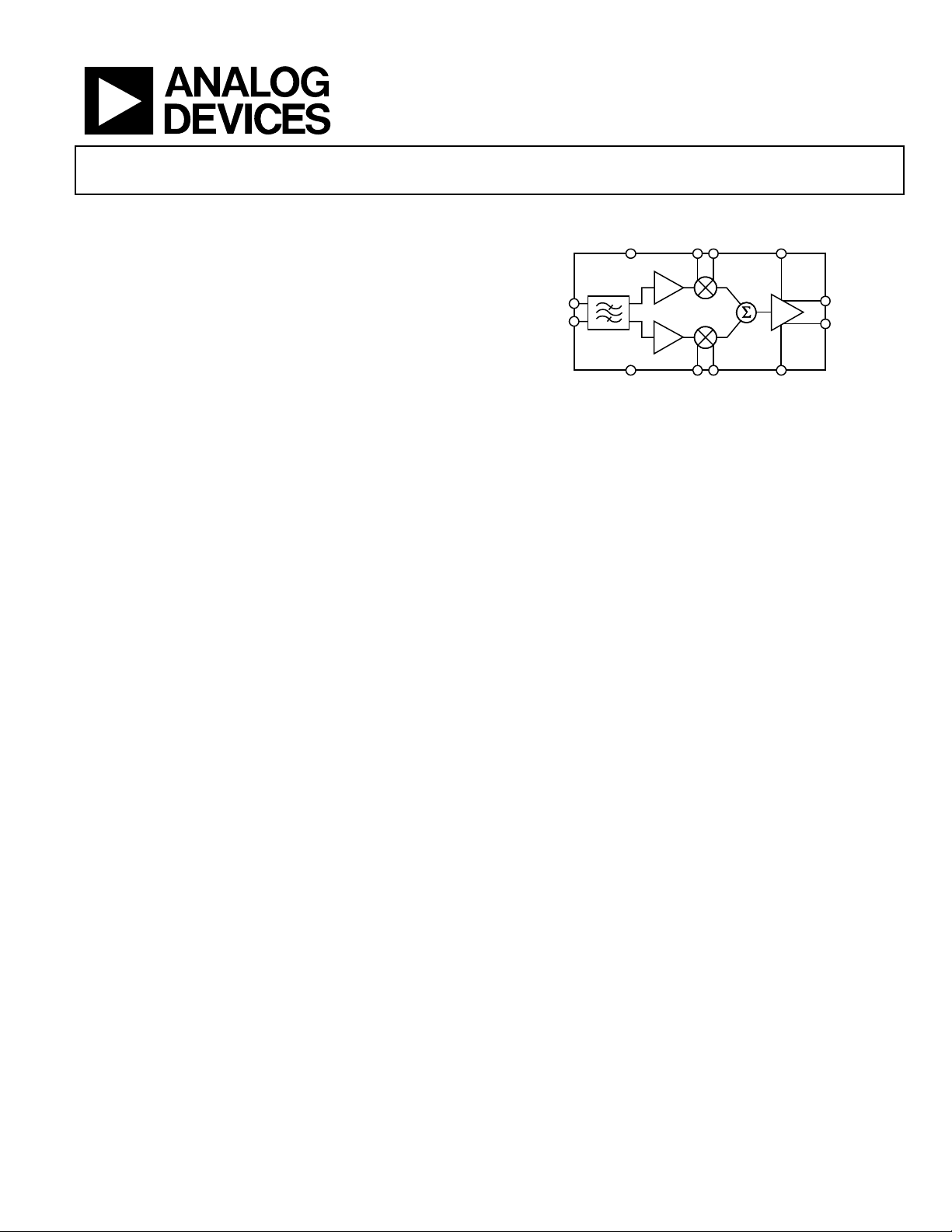
RF Vector Modulator
AD8340
FUNCTIONAL BLOCK DIAGRAM
VPRF
90°
RFIP
RFIM
0°
CMOP
Figur e 1.
Both the RF inputs and outputs can be used differentially or
single-ended and must be ac-coupled. The RF input and output
impedances are nominally 50 Ω over the operating frequency
range. The DSOP pin allows the output stage to be disabled
quickly in order to protect subsequent stages from overdrive.
The AD8340 operates off supply voltages from 4.75 V to 5.25 V
while consuming approximately 130 mA.
The AD8340 is fabricated on Analog Devices’ proprietary, high
performance 25 GHz SOI complementary bipolar IC process. It
is available in a 24-lead Pb-free LFCSP package and operates
over a −40°C to +85°C temperature range. Evaluation boards
are available.
VPS2OBBMQBBP
RFOP
RFOM
DSOPIBBMIBBP
04699-0-001
Rev. 0
Information furnished by Analog Devices is believed to be accurate and reliable.
However, no responsibility is assumed by Analog Devices for its use, nor for any
infringements of patents or other rights of third parties that may result from its use.
Specifications subject to change without notice. No license is granted by implication
or otherwise under any patent or patent rights of Analog Devices. Trademarks and
registered trademarks are the property of their respective owners.
One Technology Way, P.O. Box 9106, Norwood, MA 02062-9106, U.S.A.
Tel: 781.329.4700
Fax: 781.326.8703 © 2004 Analog Devices, Inc. All rights reserved.
www.analog.com
Page 2

AD8340
TABLE OF CONTENTS
Specifications..................................................................................... 3
RF Frequency Range.................................................................. 11
Absolute Maximum Ratings............................................................ 4
ESD Caution.................................................................................. 4
Pin Configuration and Function Descriptions............................. 5
Typical Performance Characteristics ............................................. 6
Theory of Operation ...................................................................... 10
RF Quadrature Generator......................................................... 10
I-Q Attenuators and Baseband Amplifiers.............................. 11
Output Amplifier........................................................................ 11
Noise and Distortion.................................................................. 11
Gain and Phase Accuracy .......................................................... 11
REVISION HISTORY
6/04—Revision 0: Initial Version
Applications..................................................................................... 12
Using the AD8340 ...................................................................... 12
RF Input and Matching ............................................................. 12
RF Output and Matching .......................................................... 13
Driving the I-Q Baseband Controls......................................... 13
Interfacing to High Speed DACs.............................................. 14
CDMA2000 Application............................................................ 14
Evaluation Board............................................................................ 16
Outline Dimensions....................................................................... 20
Ordering Guide .......................................................................... 20
Rev. 0 | Page 2 of 20
Page 3

AD8340
SPECIFICATIONS
V = 5 V, T = 25°C, Z = 50 Ω, f = 880 MHz, single-ended, ac-coupled source drive to RFIP through 5.6 nH series inductor, RFIM
S A O
ac-coupled through 5.6 nH series inductor to common, differential-to-single-ended conversion at output using 1:1 balun.
Table 1.
Parameter Conditions Min Typ Max Unit
OVERALL FUNCTION
Frequency Range 700 1000 MHz
Maximum Gain Maximum gain setpoint for all phase setpoints −2 dB
Minimum Gain V
Gain Control Range Relative to maximum gain 30 dB
Phase Control Range Over 30 dB control range 360 °
Gain Flatness Over any 60 MHz bandwidth 0.25 dB
Group Delay Flatness Over any 60 MHz bandwidth 10 ps
RF INPUT STAGE RFIM, RFIP (Pins 21 and 22)
Input Return Loss From RFIP to CMRF (with 5.6 nH series inductors) 20 dB
CARTESIAN CONTROL INTERFACE (I & Q) IBBP, IBBM, QBBP, QBBM (Pins 16, 15, 3, 4)
Gain Scaling 2 1/V
Modulation Bandwidth 250 mV p-p sinusoidal baseband input single-ended 230 MHz
Second Harmonic Distortion 250 mV p-p, 1 MHz, sinusoidal baseband input differential 47 dBc
Third Harmonic Distortion 250 mV p-p, 1 MHz, sinusoidal baseband input differential 45 dBc
Step Response
RF OUTPUT STAGE RFOP, RFOM (Pins 9, 10)
Output Return Loss Measured through balun 7.5 dB
f = 880 MHz
Gain Maximum gain setpoint −2 dB
Output Noise Floor Maximum gain setpoint, no input −149 dBm/Hz
P
Output IP3 f1 = 880 MHz, f2 = 877.5 MHz, maximum gain setpoint 24 dBm
ACPR
Output 1 dB Compression Point Maximum gain 11 dBm
POWER SUPPLY VPS2 (Pin 5, 6, 14); RFOP, RFOM (Pins 9, 10)
Positive Supply Voltage 4.75 5 5.25 V
Total Supply Current Includes load current 110 130 150 mA
OUTPUT DISABLE DSOP (Pin 13)
Disable Threshold 2.5 V
Maximum Attenuation DSOP = 5 V 40 dB
Enable Response Time
Disable Response Time
= V
BBI
For gain setpoint from 0.1 to 0.9
(V
For gain setpoint from 0.9 to 0.1
(V
IN
IS-95, single carrier, P
= 0 V −32 dB
BBQ
45 ns
= 0.5 V, V
BBP
= 0.55 V to 0.95 V)
BBM
47 ns
= 0.5 V, V
BBP
= 0.95 V to 0.55 V)
BBM
= 0 dBm, frequency offset = 20 MHz −147 dBm/Hz
= 0 dBm, maximum gain,
OUT
62 dBc
phase setpoint = 45°
Delay following high-to-low transition until device
15 ns
meets full specifications
Delay following low-to-high transition until device
10 ns
produces full attenuation
Rev. 0 | Page 3 of 20
Page 4
AD8340
ABSOLUTE MAXIMUM RATINGS
Table 2.
Parameters Rating
Supply Voltage VPRF, VPS2 5.5 V
DSOP 5.5 V
IBBP, IBBM, QBBP, QBBM 2.5 V
RFOP, RFOM 5.5V
RF Input Power at Maximum Gain 13 dBm, re: 50 Ω
(RFIP or RFIM, Single-Ended Drive)
Equivalent Voltage 2.8 V p-p
Internal Power Dissipation 825 mW
θJA (With Pad Soldered to Board) 59 °C/W
Maximum Junction Temperature 125°C
Operating Temperature Range −40°C to +85°C
Storage Temperature Range −65°C to +150°C
Lead Temperature Range (Soldering 60 sec) 300°C
ESD CAUTION
ESD (electrostatic discharge) sensitive device. Electrostatic charges as high as 4000 V readily accumulate on the
human body and test equipment and can discharge without detection. Although this product features proprietary ESD protection circuitry, permanent damage may occur on devices subjected to high energy electrostatic
discharges. Therefore, proper ESD precautions are recommended to avoid performance degradation or loss of
functionality.
Stresses above those listed under Absolute Maximum Ratings
may cause permanent damage to the device. This is a stress
rating only; functional operation of the device at these or any
other conditions above those indicated in the operational
section of this specification is not implied. Exposure to absolute
maximum rating conditions for extended periods may affect
device reliability.
Rev. 0 | Page 4 of 20
Page 5

AD8340
PIN CONFIGURATION AND FUNCTION DESCRIPTIONS
VPRF
CMRF
RFIP
RFIM
CMRF
2322212019
PIN 1
INDICATOR
11
10
RFOP
RFOM
CMOP
CMOP
VPRF
12
CMOP
18
17
16
15
14
13
IFLP
IFLM
IBBP
IBBM
VPS2
DSOP
04699-0-002
24
QFLP
1
2
QFLM
3
QBBP
QBBM
VPS2
VPS2
4
5
6
AD8340
TOP VIEW
(Not to Scale)
789
CMOP
Figure 2. 24-Lead Lead Frame Chip Scale Package (LFCSP)
Table 3. Pin Function Descriptions
Pin No. Mnemonic Function
1, 2 QFLP, QFLM
Q Baseband Input Filter Pins. Connect optional capacitor to reduce Q baseband channel low-pass
corner frequency.
3, 4 QBBP, QBBM Q Channel Differential Baseband Inputs.
5, 6, 14, 19, 24 VPS2, VPRF Positive Supply Voltage. 4.75 V − 5.25 V.
7, 8, 11, 12, 20, 23 CMOP, CMRF Device Common. Connect via lowest possible impedance to external circuit common.
9, 10 RFOP, RFOM Differential RF Outputs. Must be ac-coupled. Differential impedance 50 Ω nominal.
13 DSOP Output disable. Pull high to disable output stage.
15, 16 IBBM, IBBP I Channel Differential Baseband Inputs.
17, 18 IFLM, IFLP
I Baseband Input Filter Pins. Connect optional capacitor to reduce I baseband channel low-pass
corner frequency.
21, 22 RFIM, RFIP Differential RF Inputs. Must be ac-coupled. Differential impedance 50 Ω nominal.
Rev. 0 | Page 5 of 20
Page 6
AD8340
TYPICAL PERFORMANCE CHARACTERISTICS
0
–5
–10
–15
–20
GAIN (dB)
–25
–30
–35
–40
0.1
0 0.3 0.5 0.9 1.00.80.70.60.40.2
Figure 3. Gain Magnitude vs. Gain Setpoint at Different Phase Setpoints,
4
3
2
1
0
–1
–2
–3
–4
–5
GAIN CONFORMANCE ERROR (dB)
–6
–7
0 0.1 1.00.2 0.3 0.4 0.5 0.6 0.7 0.8
Figure 4. Gain Conformance E rror vs. Gain Setpoint at
0
–2
–4
–6
–8
–10
–12
GAIN (dB)
–14
–16
–18
–20
–22
–24
Figure 5. Gain Magnitude vs. Phase Setpoint at Different Gain Setpoints
PHASE SETPOINT = 0°
PHASE SETPOINT = 270°
PHASE SETPOINT = 180°
GAIN SETPOINT
RF Frequency = 880 MHz
PHASE SETPOINT = 135°
PHASE SETPOINT = 45°
PHASE SETPOINT = 90°
PHASE SETPOINT = 0°
PHASE SETPOINT = 315°
PHASE SETPOINT = 270°
PHASE SETPOINT = 180°
PHASE SETPOINT = 225°
GAIN SETPOINT
Different Phase Setpoints
GAIN SETPOINT = 1.0
GAIN SETPOINT = 0.5
GAIN SETPOINT = 0.1
45
PHASE SETPOINT (Degrees)
PHASE SETPOINT = 90°
0.9
315270 36018090 135 2250
04699-0-003
04699-0-004
04699-0-005
0.4
0.2
0.0
–0.2
–0.4
–0.6
–0.8
–1.0
–1.2
–1.4
–1.6
GAIN CONFORMANCE ERROR (dB)
–1.8
–2.0
GAIN SETPOINT = 0.1
45 315270 36018090 135 2250
PHASE SETPOINT (Degrees)
GAIN SETPOINT = 1.0
GAIN SETPOINT = 0.5
Figure 6. Gain Conformance Error vs. Phase Setpoint at Diffe rent Gain Setpoints
360
330
300
270
240
210
180
GAIN SETPOINT = 0.1
150
PHASE (Degrees)
120
90
60
30
0
0 30 60 90 120 150 180 210 240 270 300 330 360
GAIN SETPOINT = 1.0
GAIN SETPOINT = 0.5
PHASE SETPOINT (Degrees)
Figure 7. Phase vs. Phase Setpo int at Different Gain Setpoi nts
6
4
2
0
–2
–4
–6
PHASE ERROR (Degrees)
–8
–10
–12
0 45 90 135 360180 225 270 315
GAIN SETPOINT = 0.1
GAIN SETPOINT = 1.0
GAIN SETPOINT = 0.5
04699-0-008
PHASE SETPOINT (Degrees)
Figure 8. Phase Error vs. Phase Setpoint at D ifferent Gain Setpoints
04699-0-006
04699-0-007
Rev. 0 | Page 6 of 20
Page 7

AD8340
–142
–143
–144
–145
–146
–147
–148
–149
NOISE FLOOR (dBm/Hz)
–150
–151
–152
0.1
0 0.3 0.5 0.9 1.00.80.70.60.40.2
RF PIN = +5dBm
RF PIN = –5dBm
RF PIN = 0dBm
NO RF INPUT
GAIN SETPOINT
Figure 9. Output Noise Floor vs. Gain, Noise in dBm/Hz, No Carrier,
With Carrier (20 MHz Offset ) Pin = −5, 0, and +5 dBm
0
–2
–4
–6
–8
–10
–12
GAIN (dB)
–14
–16
–18
–20
–22
–24
700 1000950900850800750
GAIN SETPOINT = 1.0
GAIN SETPOINT = 0.5
GAIN SETPOINT = 0.1
04699-0-010
FREQUENCY (MHz)
Figure 10. Gain vs. Frequency at Different Gain Setpoints (700 MHz to 1000 MHz),
Phase Setpoint = 0°
–145
–146
04699-0-009
0
–0.5
–1.0
–1.5
GAIN FLATNESS (dB)
–2.0
–2.5
700 750 800 850 1000900 950
FREQUENCY (MHz)
Figure 12. Gain Flatness vs. Frequency, Maximum Gain, Phase Setpoint = 0°
0
–10
–20
–30
–40
–50
–60
–70
–80
–90
RF OUTPUT AM SIDEBAND POWER (dBm)
–100
100 200 300 400 500 600 700 800 900 1000
FUNDAMENTAL POWER, 879MHz, 881MHz
SECOND BASEBAND HARMONIC PRODUCT,
878MHz, 882MHz
THIRD BASEBAND HARMONIC PRODUCT,
877MHz, 883MHz
DIFFERENTIAL BASEBAND INPUT LEVEL (mV p-p)
(I OR Q CHANNEL DRIVEN AT 1MHz)
Figure 13. Baseband Harmonic Distortion (I and Q Channel, RF Input = 0 dBm,
Balun and Cable Losses of Approximately 2 dB Not Accounted for in Plot)
14
12
TEMP = +25°C
TEMP = –40°C
04699-0-012
04699-0-013
–147
–148
–149
NOISE (dBm/Hz)
–150
–151
–152
700 750 800 850 1000900 950
RF FREQUENCY (MHz)
Figure 1 1. Output Noise Floo r vs. Freque ncy, Maximu m Gain,
No RF Carrier, Phase Setpoint = 0°
04699-0-011
Rev. 0 | Page 7 of 20
10
8
6
OP1dB (dBm)
4
2
0
700 750 800 850 1000900 950
FREQUENCY (MHz)
TEMP = +85°C
Figure 14. Output 1dB Compression Point vs. Frequency and Temperature,
Maximum Gain, Phas e Setpoint = 0°
04699-0-014
Page 8

AD8340
30
28
26
24
22
20
OIP3 (dBm)
18
16
14
12
10
700 750 800 850 1000900 950
TEMP = +85°C
FREQUENCY (MHz)
Figure 15. Output IP3 vs. Frequency and Temperature, Maximum Ga in, I Only
0
–5
1V p-p BB INPUT
–10
500mV p-p BB INPUT
–15
–20
–25
RF OUTPUT AM SIDEBAND POWER (dBm)
–30
0 50 100 150 400200 250 300 350
200mV p-p BB INPUT
FREQUENCY (MHz)
Figure 16. I/Q Modulation Bandwidth vs. Baseband Magnitude
14
12
10
8
6
4
2
0
–2
OP1dB (dBm)
–4
–6
–8
–10
–12
0
GAIN SETPOINT = 1.0
GAIN SETPOINT = 0.5
GAIN SETPOINT = 0.1
9045
180
135
PHASE SETPOINT (Degrees)
Figure 17. Output 1dB Compression Point vs. Gain and Phase Setpoints
225
TEMP = –40°C
TEMP = +25°C
315
270
360
04699-0-015
04699-0-016
04699-0-017
30
25
20
15
OIP3 (dBm)
10
5
0
0 45 90 135 360180 225 270 315
GAIN SETPOINT = 1.0
GAIN SETPOINT = 0.5
GAIN SETPOINT = 0.1
PHASE SETPOINT (Degrees)
Figure 18. Output IP3 vs. Gain and Phase Setpoints, 2.5 MHz Carrier Sp acing
RBW 30kHz
REF LVL
0 dBm
0
–10
–20
–30
–40
–50
–60
–70
OUTPUT POWER (dBm)
–80
SECOND BASEBAND HARMONIC
–90
–100
CENTER 880 MHz 500 kHz/ SPAN 5 MHz
DESIRED SIDEBAND
VBW 30kHz
SWT 100ms
RF FEEDTHROUGH
FREQUENCY (MHz)
RF ATT 20dB
MIXER –10dBm
UNIT dBm
UNDESIRED SIDEBAND
A
1 RM
SECOND BASEBAND HARMONIC
04699-0-019
Figure 19. Single-Sideband Performance, 880 MHz, −10 dBm RF Input;
1 MHz, 500 mV p-p Differential BB Drive
90
60
500MHz
300
30
330
0
04699-0-020
180
150
210
120
1.5GHz
1.5GHz
500MHz
240
270
IMPEDANCE CIRCLE
S11 RF PORT WITH 5.6nH INDUCTORS
S11 RF PORT WITHOUT INDUCTORS
Figure 20. Input and Output Impedance Smith Chart (with Frequency Markers)
04699-0-018
Rev. 0 | Page 8 of 20
Page 9

AD8340
90
500MHz
300
60
30
0
330
180
150
210
120
1.5GHz
500MHz
1.5GHz
240
270
IMPEDANCE CIRCLE
S22 PORT WITH 1 TO 1 TRANSFORMER
SDD22 PORT DIFFERENTIAL
Figure 21. Output Impedance Smith Chart (with Frequency Markers)
6
4
2
0
–2
–4
–6
–8
PHASE ERROR (Degrees)
–10
–12
–14
PHASE SETPOINT = 45°
PHASE SETPOINT = 0°
PHASE SETPOINT = 90°
1.00 0.1 0.2 0.3 0.4 0.5 0.6 0.7 0.8 0.9
GAIN SETPOINT
Figure 22. Phase Error vs. Gain Setpoint by Phase Setpoint, 5 V dc, 25°C, 880 MHz
135
134
133
132
131
130
129
128
SUPPLY CURRENT (mA)
127
126
125
5.25V
5V
4.75V
20
TEMPERATURE (°C)
4030
60 70 8050–40 –30 –20 –10 0 10
Figure 23. Supply Current vs. Temperature
04699-0-021
04699-0-022
04699-0-023
0
–5
–10
–15
–20
–25
–30
–35
RF OUTPUT POWER (dBm)
–40
–45
–50
0.5
0 1.5 2.5 4.5 5.04.03.53.02.01.0
Figure 24. Power Shutdown Attenuation
TEK FAST ACQ SAMPLE
200mV/DIV
CHAN 1/3 (V)
3
RF OUTPUT
CH1 200mV Ω
CH3 2.0V
Figure 25. Power Shutdown Response Time
DSOP VOLTAGE (V)
M 10.0ns 5.0GS/s
A CH2 160mV
TIME (10ns/DIV)
2V/DIV
DSOP
ET 200ps/pt 74.0ns
04699-0-024
04699-0-025
Rev. 0 | Page 9 of 20
Page 10

AD8340
(
)
V
THEORY OF OPERATION
The AD8340 is a linear RF vector modulator with Cartesian
baseband controls. In the simplified block diagram given in
Figure 26, the RF signal propagates from the left to the right
while baseband controls are placed above and below. The RF
input is first split into in-phase (I) and quadrature (Q) components. The variable attenuators independently scale the I and Q
components of the RF input. The attenuator outputs are then
summed and buffered to the output.
By controlling the relative amounts of I and Q components that
are summed, continuous magnitude and phase control of the
gain is possible. Consider the vector gain representation of the
AD8340 expressed in polar form in Figure 27. The attenuation
factors for the I and Q signal components are represented on
BBI
and
BBI
and
the x- and y-axis, respectively, by the baseband inputs, V
. The resultant of their vector sum represents the vector
V
BBQ
gain, which can also be expressed as a magnitude and phase. By
applying different combinations of baseband inputs, any vector
gain within the unit circle can be programmed.
or V
A change in sign of V
BBI
can be viewed as a change in
BBQ
sign of the gain or as a 180° phase change. The outermost
circle represents the maximum gain magnitude of unity. The
circle origin implies, in theory, a gain of 0. In practice, circuit
mismatches and unavoidable signal feedthrough limit the
minimum gain to approximately −40 dB. The phase angle
between the resultant gain vector and the positive x-axis is defined as the phase shift. Note that there is a nominal, systematic
insertion phase through the AD8340 to which the phase shift is
added. In the following discussions, the systematic insertion
phase is normalized to 0°.
The correspondence between the desired gain and phase setpoints, Gain
V
, is given by simple trigonometric identities
BBQ
and PhaseSP, and the Cartesian inputs, V
SP
2
()
[]
SP
BBI
()
VVPhase /arctan=
BBI
BBQSP
//
VVVVGain +=
OBBQO
2
where:
V
is the baseband scaling constant (500 mV).
O
V
and V
BBI
are the differential I and Q baseband voltages,
BBQ
respectively.
Note that when evaluating the arctangent function, the proper
phase quadrant must be selected. For example, if the principal
value of the arctangent (known as the Arctangent(x)) is used,
quadrants 2 and 3 would be interpreted mistakenly as quadrants
4 and 1, respectively. In general, both V
and V
BBI
are needed
BBQ
in concert to modulate the gain and the phase.
Pure amplitude modulation is represented by radial movement
of the gain vector tip at a fixed angle, while pure phase modulation is represented by rotation of the tip around the circle at a
fixed radius. Unlike traditional I-Q modulators, the AD8340 is
designed to have a linear RF signal path from input to output.
Traditional I-Q modulators provide a limited LO carrier path
through which any amplitude information is removed.
BBI
LINEAR
ATTENUATOR
LINEAR
ATTENUATOR
VBBQ
V
q
+0.5
|A|
–0.5
A
θ
I-V
OUTPUT
DISABLE
SINGLE-ENDED OR
DIFFERENTIAL
50Ω OUTPUT
V
i
+0.5–0.5
04699-0-027
SINGLE-ENDED OR
DIFFERENTIAL
50Ω INPUT Z
MIN GAIN < –30dB
I CHANNEL INPUT
V-I
0°/90°
V-I
Q CHANNEL INPUT
Figure 26. Simplified Architecture of the AD8340
MAX GAIN = 0dB
Figure 27. Vector Gain Representation
RF QUADRATURE GENERATOR
The RF input is directly coupled differentially or single-ended
to the quadrature generator, which consists of a multistage RC
polyphase network tuned over the operating frequency range of
700 MHz to 1000 MHz. The recycling nature of the polyphase
network generates two replicas of the input signal, which are in
precise quadrature, i.e., 90°, to each other. Since the passive
network is perfectly linear, the amplitude and phase information
contained in the RF input is transmitted faithfully to both channels. The quadrature outputs are then separately buffered to
drive the respective attenuators. The characteristic impedance
of the polyphase network is used to set the input
impedance to the AD8340.
04699-0-026
Rev. 0 | Page 10 of 20
Page 11

AD8340
I-Q ATT ENUATO R S AN D BA SEBAND AMPLIFIERS
The proprietary linear-responding attenuator structure is an
active solution with differential inputs and outputs that offer
excellent linearity, low noise, and greater immunity from mismatches than other variable attenuator methods. The gain, in
linear terms, of the I and Q channels is proportional to its control
voltage with a scaling factor designed to be 2/V, i.e., a full-scale
gain setpoint of 1.0 (−2 dB) for V
of 500 mV. The control
BBI (Q)
voltages can be driven differentially or single-ended. The combination of the baseband amplifiers and attenuators allows for
maximum modulation bandwidths in excess of 200 MHz.
OUTPUT AMPLIFIER
The output amplifier accepts the sum of the attenuator outputs
and delivers a differential output signal into the external load.
The output pins must be pulled up to an external supply,
preferably through RF chokes. When the 50 Ω load is taken
differentially, an output P1dB and IP3 of 11 dBm and 24 dBm is
achieved, respectively, at 880 MHz. The output can be taken in
single-ended fashion, albeit at lower performance levels.
NOISE AND DISTORTION
The output noise floor and distortion levels vary with the gain
magnitude but do not vary significantly with the phase. At the
higher gain magnitude setpoints, the OIP3 and the noise floor
vary in direct proportion with the gain. At lower gain magnitude setpoints, the noise floor levels off while the OIP3
continues to vary with the gain.
GAIN AND PHASE ACCURACY
There are numerous ways to express the accuracy of the
AD8340. Ideally, the gain and phase should precisely follow the
setpoints. Figure 3 illustrates the gain error in dB from a best fit
line, normalized to the gain measured at the gain setpoint = 1.0,
for the different phase setpoints. Figure 6 shows the gain error
in a different form; the phase setpoint is swept from 0° to 360°
for different gain setpoints. Figure 8 and Figure 22 show analogous errors for the phase error as a function of gain and phase
setpoints. The accuracy clearly depends on the region of operation within the vector gain unit circle. Operation very close to
the origin generally results in larger errors as the relative
accuracy of the I and Q vectors degrades.
RF FREQUENCY RANGE
The frequency range on the RF input is limited by the internal
polyphase quadrature phase-splitter. The phase-splitter splits
the incoming RF input into two signals, 90° out of phase, as
previously described in the RF Quadrature Generator section.
This polyphase network has been designed to ensure robust
quadrature accuracy over standard fabrication process parameter variations for the 700 MHz to 1 GHz specified RF frequency
range. Using the AD8340 as a single-sideband modulator and
measuring the resulting sideband suppression is a good gauge
of how the quadrature accuracy is maintained over RF
frequency. A typical plot of sideband suppression from
500 MHz to 1.5 GHz is shown in Figure 28. The level of sideband suppression degradation outside the 700 MHz to 1 GHz
specified range will be subject to manufacturing process
variations.
0
–5
–10
–15
–20
–25
SB SUPPRESSION (dBc)
–30
–35
500 150014001300120011001000900800600 700
FREQUENCY (MHz)
Figure 28. Sideband Suppression vs. Frequency
04699-0-028
Rev. 0 | Page 11 of 20
Page 12

AD8340
APPLICATIONS
USING THE AD8340
The AD8340 is designed to operate in a 50 Ω impedance
system. Figure 30 illustrates an example where the RF input is
driven in a single-ended fashion while the differential RF output is converted to a single-ended output with a RF balun. The
baseband controls for the I and Q channels are typically driven
from differential DAC outputs. The power supplies, VPRF and
VPS2, should be bypassed appropriately with 0.1 µF and 100 pF
capacitors. Low inductance grounding of the CMOP and CMRF
common pins is essential to prevent unintentional peaking of
the gain.
RF INPUT AND MATCHING
The input impedance of the AD8340 is defined by the characteristics of the polyphase network. The capacitive component of
the network causes its impedance to roll-off with frequency
albeit at a slower rate than 6 dB/octave. By using matching
inductors on the order of 5.6 nH in series with each of the RF
inputs, RFIP and RFIM, a 50 Ω match is achieved with a return
loss of >10 dB over the operating frequency range. Different
matching inductors can improve matching over a narrower
frequency range. The single-ended and differential input
impedances are exactly the same.
5.6nH
RF
50Ω
100pF
100pF
5.6nH
RFIM
~1VDC
RFIP
PHASE
Figure 29. RF Input Interface to the AD8340 Showing
Coupling Capacitors and Matching Inductors
The RFIP and RFIM should be ac-coupled through low loss
series capacitors as shown in Figure 29. The internal dc levels
are at approximately 1 V. For single-ended operation, one input
is driven by the RF signal while the other input is ac grounded.
VP
RC
04699-0-029
IBBM
IBBP
INPUT
QBBP
QBBM
VP
RF
VP
C3
0.1µF
C6
100pF
C5
100pF
C8
0.1µF
100pF
L3
5.6nH
L4
5.6nH
C4
C7
100pF
C12
(SEE TEXT)
IFLP
VPRF
CMRF
RFIM
RFIP
CMRF
VPRF
P
L
Q
F
C11
(SEE TEXT)
IFLM
AD8340
QFLM
100pF
IBBP
QBBP
C2
IBBM
QBBM
DSOP
VPS2
VPS2
VPS2
C9
100pF
C1
0.1µF
CMOP
CMOP
RFOM
RFOP
CMOP
CMOP
C10
0.1µF
120nH
L1
VP
A
OUTPUT
DISABLE
B
L2
120nH
C14
0.1µF
C17
100pF
C18
100pF
VP
ETC1-1-13
RF
OUTPUT
04699-0-030
Figure 30. Basic Connections
Rev. 0 | Page 12 of 20
Page 13

AD8340
–
RF OUTPUT AND MATCHING
The RF outputs of the AD8340, RFOP and RFOM, are open
collectors of a transimpedance amplifier which need to be
pulled up to the positive supply, preferably with RF chokes as
shown in Figure 31. The nominal output impedance looking
into each individual output pin is 25 Ω. Consequently, the
differential output impedance is 50 Ω.
V
P
R
T
RFOM
±I
SIG
G
M
RFOP
R
T
Figure 31. RF Output Interface to the AD8340 Showing
Coupling Capacitors, Pull-Up RF Chokes, and Balun
Since the output dc levels are at the positive supply, ac coupling
capacitors will usually be needed between the AD8340 outputs
and the next stage in the system.
A 1:1 RF broadband output balun, such as the ETC1-1-13
(M/A-COM), converts the differential output of the AD8340
into a single-ended signal. Note that the loss and balance of the
balun directly impact the apparent output power, noise floor,
and gain/phase errors of the AD8340. In critical applications,
narrow-band baluns with low loss and superior balance are
recommended.
If the output is taken in a single-ended fashion directly into a
50 Ω load through a coupling capacitor, there will be an impedance mismatch. This can be resolved with a 1:2 balun to convert
the single-ended 25 Ω output impedance to 50 Ω. If loss of
signal swing is not critical, a 25 Ω back termination in series
with the output pin can also be used. The unused output pin
must still be pulled up to the positive supply. The user may load
it through a coupling capacitor with a dummy load to preserve
balance. The gain of the AD8340 when the output is singleended varies slightly with dummy load value as shown in Figure 32.
120nH
100pF
100pF
50Ω
DIFFERENTIAL
1:1
RF
OUTPUT
04699-0-031
0.5
–1.0
–1.5
–2.0
–2.5
–3.0
–3.5
GAIN (dB)
–4.0
–4.5
–5.0
–5.5
–6.0
R
= SHORT
L2
= 50Ω
R
L2
= OPEN
R
L2
FREQUENCY (MHz)
04699-0-032
900800700
1000
Figure 32. Gain of the AD8340 Using a Single-Ended Output with Different Dummy
Loads, RL2 on the Unused O utput
The RF output signal can be disabled by raising the DSOP pin
to the positive supply. The shutdown function provides >40 dB
attenuation of the input signal even at full gain. The interface
to DSOP is high impedance and the shutdown and turn-on
response times are <100 ns. If the disable function is not
needed, the DSOP should be tied to ground.
DRIVING THE I-Q BASEBAND CONTROLS
The I and Q inputs to the AD8340 set the gain and phase between input and output. These inputs are differential and should
normally have a common-mode level of 0.5 V. However, when
differentially driven, the common mode can vary from 250 mV
to 750 mV while still allowing full gain control. Each input pair
has a nominal input swing of ±0.5 V differential around the
common-mode level. The maximum gain of unity is achieved if
the differential voltage is equal to +500 mV or −500 mV. So
with a common-mode level of 500 mV, IBBP and IBBM will
each swing between 250 mV and 750 mV.
The I and Q inputs can also be driven with a single-ended
signal. In this case, one side of each input should be tied to a
low noise 0.5 V voltage source (a 0.1 µF decoupling capacitor
located close to the pin is recommended), while the other input
swings from 0 V to 1 V. Differential drive generally offers superior even-order distortion and lower noise than single-ended
drive.
The bandwidth of the baseband controls exceeds 200 MHz even
at full-scale baseband drive. This allows for very fast gain and
phase modulation of the RF input signal. In cases where lower
modulation bandwidths are acceptable or desired, external filter
capacitors can be connected across Pins IFLP to IFLM and
QFLP to QFLM to reduce the ingress of baseband noise and
spurious signal into the control path.
Rev. 0 | Page 13 of 20
Page 14

AD8340
The 3 dB bandwidth is set by choosing C
according to the
FLT
following equation:
nF10kHz45
f
≈
3dB
C
This equation has been verified for values of C
external
×
+
pF0.5
from 10 pF to
FLT
0.1 µF (bandwidth settings of approximately 4.5 kHz to 43 MHz).
INTERFACING TO HIGH SPEED DACs
The AD977x family of dual DACs is well suited to driving the I
and Q vector controls of the AD8340. While these inputs can in
general be driven by any DAC, the differential outputs and bias
level of the ADI TxDAC® family allows for a direct connection
between DAC and modulator.
The AD977x family of dual DACs have differential current outputs. The full-scale current is user programmable and is usually
set to 20 mA, that is, each output swings from 0 mA to 20 mA.
The basic interface between the AD9777 DAC outputs and the
AD8340 I and Q inputs is shown in Figure 33. The Resistors R1
and R2 set the dc bias level according to the equation:
Bias Level = Average Output Current × R1
For example, if the full-scale current from each output is 20 mA,
each output will have an average current of 10 mA. Therefore to
set the bias level to the recommended 0.5 V, R1 and R2 should
be set to 50 Ω each. R1 and R2 should always be equal.
If R3 is omitted, this will result in an available swing from
the DAC of 2 V p-p differential, which is twice the maximum
voltage range required by the AD8340. DAC resolution can be
maximized by adding R3, which scales down this voltage
according to the following equation:
=SwingScaleFull
R2
()
MAX
AD9777 AD8340
I
OUTA1
I
OUTB1
()
R1
R2
⎡
R3R2R1I
−×+×
1||2
⎢
⎣
OPTIONAL
LOW-PASS
FILTER
⎤
⎥
+
R3R2
⎦
IBBP
R3
IBBM
1.15
1.13
1.10
1.08
1.05
1.02
1.00
0.97
0.95
0.92
0.90
0.88
0.85
0.82
0.80
0.77
0.75
DIFFERENTIAL PEAK-TO-PEAK SWING (R3)
0.72
0.70
R3
13050 55 60 65 70 75 80 85 90 100 105 115 120110 12595
04699-0-034
Figur e 34. Pe ak-to- Peak DAC Outpu t Swing vs.
Swing Scaling Resistor R3 (R1 = R2 = 50 Ω)
Figure 34 shows the relationship between the value of R3 and
the peak baseband voltage with R1 and R2 equal to 50 Ω.
From Figure 34, it can be seen that a value of 100 Ω for R3 will
provide a peak-to-peak swing of 1 V p-p differential into the
AD8340’s I and Q inputs.
When using a DAC, low-pass image reject filters are typically
used to eliminate the Nyquist images produced by the DAC.
They also provide the added benefit of eliminating broadband
noise that might feed into the modulator from the DAC.
CDMA2000 APPLICATION
To test the compliance to the CDMA2000 base station standard,
a single-carrier CDMA2000 test model signal (forward pilot,
sync, paging, and six traffic as per 3GPP2 C.S0010-B, Table
6.5.2.1) was applied to the AD8340. A cavity tuned filter was
used to reduce noise from the signal source being applied to the
device. The 4.6 MHz pass band of this filter is apparent in the
subsequent spectral plots.
Figure 35 shows a plot of the spectrum of the output signal under nominal conditions. P
0.353 V, i.e., VIBBP − VIBBM = VQBBP − VQBBM = 0.353 V.
Adjacent channel power is measured in 30 kHz resolution
bandwidth at 750 KHz and 1.98 MHz carrier offset. Noise floor
is measured at ±4 MHz carrier offset.
is equal to −5 dBm and VI = VQ =
OUT
I
OUTA2
I
OUTB2
R1
R2
OPTIONAL
LOW-PASS
FILTER
R3
Figure 33. Basic AD9777 to AD8340 Interface
QBBP
QBBM
04699-0-033
Rev. 0 | Page 14 of 20
Page 15

AD8340
BS, 1X, C0 : ADJ CHANNEL
REF –12dBm
OFFSET 0.5 dB
–20
–30
–40
–50
–60
SWP 50 OF 50
–70
–80
–90
–100
2
–110
*RBW 30kHz
*VBW 30kHz
*SWT 100ms*ATT 5dB
MARKER 2 [T1 NOI]
–148.76dBm/Hz
876.009615385MHz
CH PWR
–5.17dBm
ACP LOW
–60.94dB
ACP UP
–60.08dB
ALT1 LOW
–86.40dB
ALT1 UP
–86.80dB
MARKER 1 [T1 NOI]
–148.89dBm/Hz
884.006410256MHz
SPAN 10MHz1MHz/CENTER 880MHz
LVL
NOR
1
04699-0-035
Figure 35. Output Spectrum, Single-Carrier CDMA2000 Test Model at −5 dBm,
= VQ = 0.353 V, ACP Measured at 750 kHz and 1.98 KHz Carrier Offset,
V
I
Noise Measured at ± 4 MHz Carrier Offset, Input Sign al Filtered Using a
Cavity Tuned Filter (Pass Band = 4.6 MHz)
Holding the I and Q control voltages steady at 0.353 V, input
power was swept. Figure 36 shows the resulting output power,
noise floor, and adjacent channel power ratio. Noise floor is
presented as noise in a 1 MHz bandwidth as defined by the
3GPP2 specification.
–30
–40
–50
–60
–70
–80
ACP – dBc (30kHz RBW)
–90
–100
–30 50–5–10–15–20–25
ACP – 750kHz OFFSET, 30kHz RBW
ACP – 1.98MHz OFFSET, 30kHz RBW
NOISE – 4MHz OFFSET, 1MHz RBW
OUTPUT POWER (dBm)
Figure 36. Noise and ACP vs. Output Power, Single-Carrier CDMA2000 Test Model,
= VQ = 0.353, ACP Measured in 30 kHz RBW at ±750 kHz and ±1.98 KHz Carrier Offset,
V
I
Noise Measured at ±4 MHz Carrier Offs et
–30
–40
–50
–60
–70
–80
–90
–100
04699-0-036
NOISE – dBm @ 4MHz CARRIER OFFSET (1MHz RBW)
The results show that at an output power of +3 dBm, ACP is still
in compliance with the standard (<−45 dBc @ 750 MHz and
<−60 dBc @ 1.98 MHz). At low output power levels, ACP at
1.98 MHz carrier offset degrades as the noise floor of the
AD8340 becomes the dominant contributor to measured ACP.
Measured noise at 4 MHz carrier offset begins to increase
sharply above 0 dBm output power. This increase is not due to noise
but results from increased carrier-induced distortion. As output
power drops below 0 dBm, the noise floor drops towards −90 dBm.
With a fixed input power of 2.4 dBm, the output power was
again swept by exercising the I and Q inputs. V
and VQ were
I
kept equal and were swept from 10 mV to 500 mV. The resulting output power, ACP, and noise floor are shown in Figure 37.
10
P
vs. V
OUT
0
–10
–20
–30
–40
OUTPUT POWER (dBm)
–50
–60
–70
0 50 100 150 200 250 300 350 400 450 500
ACP – 750kHz OFFSET, 30kHz RBW
ACP – 1.98MHz OFFSET, 30kHz RBW
NOISE – 4MHz OFFSET, 1MHz RBW
IN
= VQ=VIN (mV)
V
I
–50
–55
–60
–65
–70
–75
ACP – dBc (30kHz RBW)
–80
–85
–90
NOISE – 4MHz CARRIER OFFSET – dBm (1MHz RBW)
04699-0-037
Figure 37. Output Power, Noise, and ACP vs. I and Q Control Voltages, CDMA2000 Test
= VQ, ACP Measured in 30 kHz RBW at ±750 kHz and ±1.98 kHz Carrier Offset,
Model, V
I
Noise Measured at ±4 MHz Carrier Offs et
In contrast to Figure 36, Figure 37 shows that for a fixed input
power, ACP remains fairly constant as gain and phase are
changed (this is not true for very high input powers). The noise
floor still drops with decreasing gain, but it never reaches the
−90 dBm level in Figure 37.
Figure 38 shows the output spectrum for a 3-carrier
CDMA2000 spectrum. Again, the signal being applied to the
AD8340 is filtered by a cavity-tuned filter with a −3 dB bandwidth of 4.6 MHz. To reduce distortion, the total output carrier
power has been reduced to approximately −8 dBm (per-carrier
power = −12.6 dBm). Adjacent channel power ratios of −61 dBc
(2 MHz from center of spectrum) and −82 dBc (3.23 MHz from
center of spectrum) were measured. The noise floor, measured
at 5.25 MHz carrier offset, is approximately −149 dBm/Hz
(−89 dBm in a 1 MHz bandwidth). So while some dynamic
range has been lost due to output power back-off, ACP stays
approximately equal and noise floor improves slightly.
*RBW 30kHz
*VBW 300kHz
*SWT 5s*ATT 5dBREF –15 dBm
–20
–30
–40
–50
–60
–70
–80
–90
–100
–110
OFFSET 0.5dB
Figure 38. Output Spectrum, 3-Carrier CDMA2000 Test Model at −12.5 dBm/Carrier,
VI = VQ = 0.353 V, ACP Measured at 2 MHz and 3.23 KHz Offset from Center of
Spectrum, Noise Meas ured at 5.25 MHz Carrier Offs et, Input Signal Filtered
Using a Cavity Tuned Filter (Pass Band = 4.6 MHz)
MARKER 1 [T1 NOI]
–148.83dBm/Hz
885.252403846MHz
CH1
–12.65dBm
CH2
–12.58dB
CH3
–12.87dB
TOTAL
–7.93dB
ACP LOW
–61.41dB
ACP UP
–61.87dB
ALT1 LOW
–82.36dB
ALT1 UP
–81.92dB
1
SPAN 15MHz1.5MHz/CENTER 880MHz
A
SOL
LVL
NOR
04699-0-038
Rev. 0 | Page 15 of 20
Page 16

AD8340
EVALUATION BOARD
The evaluation board circuit schematic for the AD8340 is
shown in Figure 39.
The evaluation board is configured to be driven from a
single-ended 50 Ω source. Although the input of the AD8340 is
differential, it may be driven single-ended, with no loss of
performance.
The low-pass corner frequency of the baseband I and Q channels can be reduced by installing capacitors in the C11 and C12
positions. The low-pass corner frequency for either channel is
approximated by
nF10kHz45
f
≈
3dB
C
On this evaluation board, the I and Q baseband circuits are
identical to each other, so the following description applies
equally to each. The connections and circuit configuration for
the Q baseband inputs are described in Table 4.
external
×
+
pF0.5
The baseband input of the AD8340 requires a differential voltage drive. The evaluation board is set up to allow such a drive by
connecting the differential voltage source to QBBP and QBBM.
The common-mode voltage should be maintained at approximately 0.5 V. For this configuration, Jumpers W1 to W4 should
be removed.
The baseband input of the evaluation board may also be driven
with a single-ended voltage. In this case, a bias level is provided
to the unused input from Potentiometer R10 by installing either
W1 or W2.
Setting SW1 in Position B disables the AD8340 output amplifier.
With SW1 set to Position A, the output amplifier is enabled.
With SW1 set to Position A, an external voltage signal, such as a
pulse, can be applied to the DSOP SMA connector to exercise
the output amplifier enable/disable function.
Rev. 0 | Page 16 of 20
Page 17

AD8340
Table 4. Evaluation Board Configuration Options
Components Function Default Conditions
R7, R9, R11,
R14, R15, R19,
R20, R21, C15,
C19, W3, W4
R1, R3, R10,
R12, R13, R16,
R17, R18, C16,
C20, W1, W2
C11, C12
T1, C17, C18,
L1, L2
L3, L4, C5, C6
C2, C4, C7,
C9, C14, C1,
C3, C8, C10,
R2, R4, R5, R6
R8, SW1
I Channel Baseband Interface. Resistors R7 and R9 may be installed to accommodate a
baseband source that requires a specific terminating impedance. Capacitors C15 and C19
are bypass capacitors.
For single-ended baseband drive, the Potentiometer R11 can be used to provide a bias level
to the unused input (install either W3 or W4).
Q Channel Baseband Interface. See the I Channel Baseband Interface section.
Baseband Low-Pass Filtering. By adding Capacitor C11 between QFLP and QFLM, and C12
between IFLP and IFLM, the 3 dB low-pass corner frequency of the baseband interface can
be reduced from 230 MHz (nominal). See equation in text.
Output Interface. The 1:1 balun transformer, T1, converts the 50 Ω differential output to
50 Ω single-ended. C17 and C18 are dc blocks. L1 and L2 provide dc bias for the output.
Input Interface. The input impedance of the AD8340 requires 5.6 nH inductors in series
with RFIP and RFIM for optimum return loss when driven by a single-ended 50 Ω line. C5
and C6 are dc blocks.
Supply Decoupling.
Output Disable Interface. The output stage of the AD8340 is disabled by applying a high
voltage to the DSOP pin by moving SW1 to Position B. The output stage is enabled moving
SW1 to Position A. The output disable function can also be exercised by applying an external high or low voltage to the DSOP SMA connector with SW1 in Position A.
R7, R9 = Not Installed
R11 = Potentiometer, 2 kΩ,
10 Turn (Bourns)
R14 = 4 kΩ (Size 0603)
R15 = 44 kΩ (Size 0603)
R19, R20, R21 = 0 Ω
(Size 0603)
C15, C19 = 0.1 µF
(Size 0603)
W3 = Jumper (Installed)
W4 = Jumper (Open)
R1, R3 = Not Installed
R10 = Potentiometer, 2 kΩ,
10 Turn (Bourns)
R12 = 4 kΩ (Size 0603)
R13 = 44 kΩ (Size 0603)
R16, R17, R18 = 0 Ω
(Size 0603)
C16, C20 = 0.1 µF
(Size 0603)
W1 = Jumper (Installed)
W2 = Jumper (Open)
C11, C12 = Not Installed
C17, C18 = 100 pF
(Size 0603)
T1 = ETC1-1-13 (M/A-COM)
L1, L2 = 120 nH
(Size 0603)
L3, L4 = 5.6 nH (Size 0402)
C5, C6 = 100 pF (Size 0603)
C2, C4, C7, C9, C14 = Open
(Size 0603)
C1, C3, C8, C10 = 0.1 µF
(Size 0603)
R2, R4, R5, R6 = 0 Ω
(Size 0603)
R8 = 10 kΩ (Size 0603)
SW1 = SPDT (Position A,
Output Enabled)
Rev. 0 | Page 17 of 20
Page 18

AD8340
W4
C15
0.1µF
R14
4kΩ
IFLM
AD8340
QFLM
R19
0Ω
R11
2kΩ
IBBP
QBBP
C19
0.1µF
W3
IBBM
QBBM
44kΩ
RFIN
VP
VP
C7
(OPEN)
C4
(OPEN)
C6
100pF
C5
100pF
R9
(OPEN)
R21
0Ω
C12
(OPEN)
L3
5.6nH
L4
5.6nH
C8
0.1µF
C3
0.1µF
IFLP
VPRF
CMRF
RFIM
RFIP
CMRF
VPRF
F
Q
P
L
C11
(OPEN)
R5
0Ω
R4
0Ω
R15
R7
(OPEN)
R20
0Ω
DSOP
VPS2
VPS2
VPS2
IBBMIBBP
VS
CMOP
CMOP
RFOM
RFOP
CMOP
CMOP
C10
0.1µF
R6
0Ω
TEST POINT
C2
(OPEN)
R2
0Ω
C1
0.1µF
R8
10kΩ
L1
120nH
C14
0.1µF
C9
(OPEN)
VP
SW1
L2
120nH
B
A
100pF
GND
TEST POINT
C17
100pF
C18
VP
T1
ETC1-1-13
M/A-COM
DSOP
RFOP
R12
R10
C16
2kΩ
R16
0Ω
C20
0.1µF
R13
44kΩ
W1
R18
0Ω
R3
OPEN
VS
QBBM
04699-0-039
QBBP
R17
0Ω
R1
OPEN
4kΩ
0.1µF
W2
Figure 39. Evaluation Board Schematic
Rev. 0 | Page 18 of 20
Page 19

AD8340
Figure 40. Component Side Layout
04699-0-040
Figure 41. Component Side Silkscreen
04699-0-041
Rev. 0 | Page 19 of 20
Page 20

AD8340
OUTLINE DIMENSIONS
0.08
0.60 MAX
19
18
BOTTOM
13
12
VIEW
24
7
1
6
2.50 REF
PIN 1
INDICATOR
2.25
2.10 SQ
1.95
0.25 MIN
PIN 1
INDICATOR
1.00
0.85
0.80
SEATING
PLANE
12° MAX
4.00
BSC SQ
TOP
VIEW
0.80 MAX
0.65TYP
COMPLIANT TOJEDEC STANDARDSMO-220-VGGD-2
0.30
0.23
0.18
3.75
BSC SQ
0.20 REF
0.60 MAX
0.05 MAX
0.02 NOM
0.50
BSC
0.50
0.40
0.30
COPLANARITY
Figure 42. 24-Lead Lead Frame Chip Scale Package [LFCSP]
(CP-24)
Dimensions shown in millimeters
ORDERING GUIDE
Models Temperature Range Package Description Package Option Order Multiple
AD8340ACPZ-WP
AD8340ACPZ-REEL71 −40°C to +85°C 24-Lead Lead Frame Chip Scale Package (LFCSP) CP-24 1,500
AD8340-EVAL Evaluation Board 1
1
Z = Pb-free part.
2
WP = Waffle pack.
1, 2
−40°C to +85°C 24-Lead Lead Frame Chip Scale Package (LFCSP) CP-24 64
© 2004 Analog Devices, Inc. All rights reserved. Trademarks and registered trademarks are the property of their respective owners.
D04699–0–6/04(0)
Rev. 0 | Page 20 of 20
 Loading...