

Page 1
DC to 25 MHz,
Quad I/Q Demodulator and Phase shifter
Preliminary Technical Data
FEATURES
Quad Integrated I/Q Demodulator
16 Phase Select on each Output (22.5° per step)
Quadrature Demodulation Accuracy
Phase Accuracy ±1°
Amplitude Balance ±0.25 dB
Bandwidth
4LO: LF to 100 MHz; RF: LF to 25 MHz
Baseband: determined by external filtering
Output Dynamic Range 158 dB/Hz
LO Drive > –10 dBm (50 Ω); 200 mVpp
Supply: ±5 V
Power Consumption 73 mW/channel (290 mW total)
Power Down via SPI (Each Channel and Complete Chip)
APPLICATIONS
Medical Imaging (CW Ultrasound Beamforming)
Phased Array Systems
Radar
Adaptive Antennas
Communication Receivers
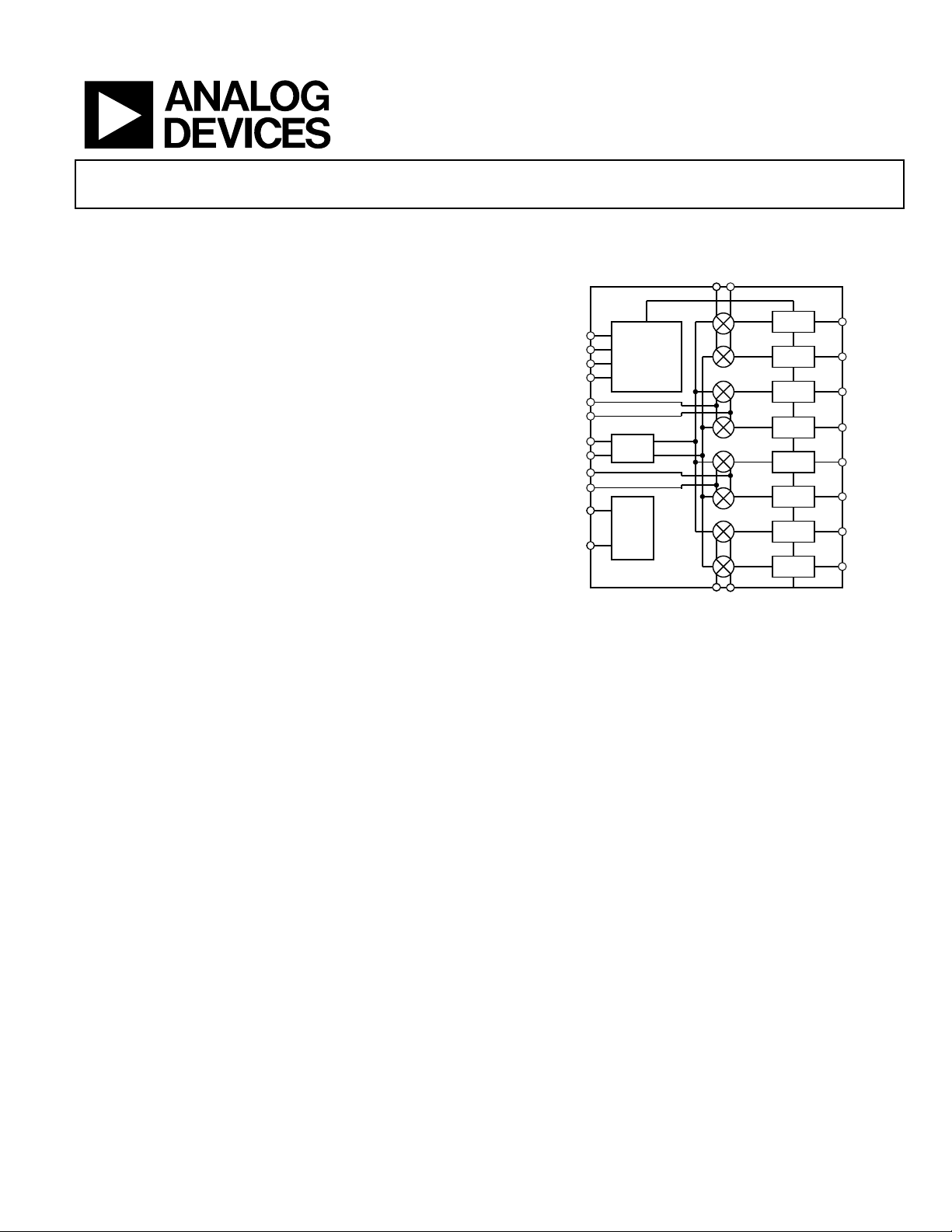
FUNCTIONAL BLOCK DIAGRAM
CH1
RF
– +
AD8339
SCLK
CH2
RF
4Х
LO
CH3
RF
VPOS
VNEG
SDI
SDO
CSB
+
–
+
–
+
–
SERIAL
INTERFACE
0°
÷4
90°
BIAS
CH4
RF
+–
AD8339
Φ
Φ Q1
Φ I2
Φ
Φ
Φ Q3
Φ I4
Φ Q4
I1
Q2
I3
GENERAL DESCRIPTION
The AD8339 is a Quad I/Q demodulator intended to be driven
by a low noise preamplifier with differential outputs; it is
optimized for the LNA in the AD8332/4/5 family of VGAs. The
part consists of four identical I/Q demodulators with a 4× local
oscillator (LO) input that divides this signal and generates the
necessary 0° and 90° phases of the internal LO that drive the
mixers. The four I/Q demodulators can be used independently
of each other (assuming that a common LO is acceptable) since
each has a separate RF input.
The major application is continuous wave (CW) analog
beamforming in ultrasound. Since in a beamforming
application the outputs of many channels are summed
coherently, the signals need to be phase aligned. A reset pin for
the LO divider that synchronizes multiple ICs to start in the
same quadrant is provided. Sixteen discrete phase rotations in
22.5° increments can be selected independently for each
channel. For example, if CH1 is used as a reference and CH2
has an I/Q phase lead of 45°, then by choosing the correct code
one can phase align CH2 with CH1.
Rev. PrB - 5/24/07
Information furnished by Analog Devices is believed to be accurate and reliable.
However, no responsibility is assumed by Analog Devices for its use, nor for any
infringements of patents or other rights of third parties that may result from its use.
Specifications subject to change without notice. No license is granted by implication
or otherwise under any patent or patent rights of Analog Devices. Trademarks and
registered trademarks are the property of their respective companies.
The mixer outputs are provided in current form so that they can
be easily summed. The summed current outputs, one each for
the I and Q signals, are externally converted to a voltage by a
high dynamic range current-to-voltage (I to V) converter. A
good choice for this transimpedance amplifier is the AD8021
because of its low noise. Following the current summation the
combined signal is presented to a high resolution AD converter
(ADC) like the AD7665 (16b/570 ksps).
An SPI compatible serial interface is provided for ease of
programming the phase of each channel; the interface allows
daisy-chaining by shifting the data through each chip from SDI
to SDO. The SPI also allows for power down of each individual
channel and the complete chip. During power down the serial
interface remains active so that the device can be programmed
again.
The dynamic range is >158 dB/Hz at the I and Q outputs. The
AD8339 is available in a 6x6 mm 40 pin LFCSP, for the
industrial temperature range of -40 C to +85 C
.
One Technology Way, P.O. Box 9106, Norwood, MA 02062-9106, U.S.A.
Tel: 781.329.4700
Fax: 781.326.8703 © 2007 Analog Devices, Inc. All rights reserved.
Figure 1. Functional Block Diagram.
www.analog.com
Page 2

AD8339 Preliminary Technical Data
TABLE OF CONTENTS
FUNCTIONAL BLOCK DIAGRAM......................................... 1
AD8339 Specifications.................................................................... 3
Absolute Maximum Ratings............................................................ 5
ESD Caution.................................................................................. 5
Pin Configuration and Function Descriptions............................. 6
Equivalent Input Circuits ................................................................ 7
Typical Performance Characteristics ............................................. 8
Test Circuits....................................................................................... 9
Theory of Operation ...................................................................... 10
Quadrature Generation ............................................................. 10
I/Q Demodulator and Phase Shifter ........................................ 11
Dynamic Range and Noise........................................................ 11
REVISION HISTORY
Summation of Multiple Channels (Analog Beamforming).. 12
Phase Compensation and Analog Beamforming................... 12
Serial Interface ............................................................................ 13
ENBL Bits ................................................................................ 13
Applications..................................................................................... 15
Logic Inputs and Interfaces....................................................... 15
Reset Input .................................................................................. 15
Evaluation Board ............................................................................ 16
Connections to the Board ......................................................... 16
Using the SPI Port .................................................................. 19
Hard-wired Jumpers .............................................................. 20
Outline Dimensions ....................................................................... 29
Rev. PrB | Page 2 of 29
Page 3

Preliminary Technical Data AD8339
AD8339 SPECIFICATIONS
Table 1. VS = ±5 V, TA = 25°C, 4×f
unless otherwise noted. Single channel AD8021 LPF values R
= 20 MHz, f
LO
= 5.01 MHz, f
RF
= 10 kHz, P
BB
= 1.58 kΩ and C
FILT
≥ 0 dBm, per channel performance, dBm (50 Ω)
LO
= 1 nF (see Figure 9).
FILT
Parameter Conditions Min Typ Max Unit
OPERATING CONDITIONS
Local Oscillator Frequency Range 4× Internal LO at pins 4LOP and 4LON
Square wave LF 100 MHz
Sine wave TBD 100 MHz
RF Frequency Range Mixing LF 25 MHz
Baseband Bandwidth Limited by external filtering LF 25 MHz
LO Input Level 0 13 dBm
V
(VS)
SUPPLY
±4.5 ±5 ±5.5
Temperature Range -40 +85
V
°C
DEMODULATOR PERFORMANCE
Input Impedance RF—Differential 7||7
LO—Differential 100||1
Transconductance
Demodulated I
; each Ix or Qx output after
OUT/VIN
kΩ||pF
kΩ||pF
low—pass filtering measured from RF inputs
All phases 1.1 mS
Dynamic Range IP1dB minus input referred noise (dBm) 158
dB (1Hz
BW)
Max Input Swing
Differential; inputs biased at 2.5V; pins RFxP,
2.7 Vpp
RFxN
Peak Output Current (No Filtering)
Input P1dB
Third Order Intermodulation (IM3)
0° Phase shift ±2.4
45° Phase shift ±3.3
Ref = 50 Ω
Ref = 1V
f
RMS
= 5.010 MHz, f
RF1
= 5.015 MHz, fLO = 5.023
RF2
14.5 dBm
1.5 dBV
mA
mA
MHz
Equal Input Levels Baseband tones: -7 dBm @ 8 kHz and 13 kHz -75 dBc
Unequal Input Levels
Baseband tones: -1 dBm @ 8 kHz and -31 dBm
TBD dBc
@13 kHz
Third Order Input Intercept (IIP3) Same conditions as IM3 30 dBm
LO Leakage
Measured at RF inputs, worst phase, measured
TBD dBm
into 50 •
Measured at baseband outputs, worst phase,
TBD dBm
AD8021 disabled, measured into 50 •
Conversion Gain All codes, see Figure XX 4.7 dB
Input Referred Noise
Output Current Noise
Output Noise ÷ Conversion Gain (see Figure XX)
Output noise ÷ 1.58 kΩ
TBD
TBD
nV/√Hz
pA/√Hz
Noise Figure With AD8332 LNA
= 50 Ω, RFB = ∞
R
S
= 50 Ω, RFB = 1.1k Ω
R
S
= 50 Ω, RFB = 274 Ω
R
S
TBD dB
TBD dB
Bias Current Pins 4LOP and 4LON -2
Pins RFxP and RFxN -35
TBD dB
μA
μA
LO Common Mode Range Pins 4LOP and 4LON (each pin) 0.2 3.8 V
RF Common Mode Voltage
For maximum differential swing; Pins RFxP and
2.5 V
RFxN (DC-coupled to AD8332 output)
Output Compliance Range Pins IxOP and QxOP -1.5 0.7 V
Rev. PrB Page 3 of 29
Page 4

AD8339 Preliminary Technical Data
PHASE ROTATION PERFORMANCE One CH is reference, others are stepped
Phase Increment 16 Phase Steps per Channel 22.5
Quadrature Phase Error
I/Q Amplitude Imbalance
Channel-to-Channel Matching
Ix to Qx; all phases, 1σ ±1
Ix to Qx; all phases, 1σ
Phase Match I-to-I and Q-to-Q; -40°C < T
Ampl. Match I-to-I and Q-to-Q; -40°C < T
< 85°C ±1
A
< 85°C ±0.5
A
0.25 dB
LOGIC INTERFACES Pins SDI,CSB,SCLK, RSTS,RSET
Logic Level High 1.5 V
Logic Level Low 0.9 V
Bias Current Logic high (pulled to +5V) 0.5
Logic low (pulled to GND) 0
Input Resistance 4
LO Divider RSET Setup Time
RSET rising edge to 4LOP-4LON (Differential)
5 ns
rising edge
LO Divider RSET High Pulse Width 20 ns
LO Divider RSET Setup Time
RSET falling edge prior to 4LOP-4LON
5 ns
(Differential) rising edge
Phase Response Time Measured from CSB going high TBD
Enable Response Time
Measured from CSB going high (with 0.1 μF cap
15
on pin LODC)
Output Pin SDO
Logic Level High Loaded with 5 pF and next SDI input 1.7 1.9 V
Logic Level Low Loaded with 5 pF and next SDI input 0.2 0.5 V
SPI TIMING CHARACTERISTICS
SCLK Frequency f
CSB to SCLK Setup Time T
Pins SDI,SDO,CSB,SCLK, RSTS
CLK
1
TBD ns
SCLK High Pulse Width T2 TBD ns
SCLK Low Pulse Width T3 TBD ns
Data Access Time after SCLK Falling Edge T
4
Data Setup Time Prior to SCLK Rising Edge T5 TBD ns
Data Hold Time after SCLK Rising Edge T6 TBD ns
CSB High Pulse Width T7 TBD ns
SCLK Fall to CSB Fall Hold Time T8 TBD ns
SCLK Fall to CSB Rise Hold Time T9 TBD
POWER SUPPLY Pins VPOS,VNEG
Supply Voltage
±4.5 ±5 ±5.5
Quiescent Current VPOS, all phase bits = 0 37.5 mA
VNEG, all phase bits = 0 -21 mA
Over Temperature
-40°C < T
< 85°C
A
TBD TBD mA
Quiescent Power Per Channel, all phase bits = 0 73 mW
Per Channel max (depends on phase bits) TBD mW
Disable Current All Channels Disabled; SPI stays on 2.6 mA
PSRR VPOS to Ix/Qx outputs (meas. @ AD8021 output) TBD dB
VNEG to Ix/Qx outputs (meas. @ AD8021 output) TBD dB
°
°
°
dB
μA
μA
MΩ
μs
μs
10 MHz
TBD ns
V
Rev. PrB| Page 4 of 29
Page 5
AD8339 Preliminary Technical Data
ABSOLUTE MAXIMUM RATINGS
Table 2.
Parameter Rating
Voltages
Supply Voltage V
S
±6 V
RF Inputs +6 V, GND
4LO Inputs +6 V, GND
Outputs (IxOP, QxOP) +1 V, -6 V
Digital Inputs +6 V, GND
SDO Output +6 V, GND
LODC Pin +6 V (max)
VPOS –1.5 V (min)
Thermal Data —4 Layer Jedec Board
No Air Flow (Exposed Pad Soldered
to PC Board)
θ
JA
θ
JB
θ
JC
Ψ
JT
Ψ
JB
Maximum Junction Temperature
TBD°C/W
TBD°C/W
TBD°C/W
TBD°C/W
TBD°C/W
150°C
Maximum Power Dissipation TBD W
(Exposed Pad Soldered to PC Board)
Operating Temperature Range
Storage Temperature Range
–40°C to +85°C
–65°C to +150°C
Lead Temperature Range (Soldering 60 sec) 300°C
Stresses above those listed under Absolute Maximum Ratings
may cause permanent damage to the device. This is a stress
rating only; functional operation of the device at these or any
other conditions above those indicated in the operational
section of this specification is not implied. Exposure to absolute
maximum rating conditions for extended periods may affect
device reliability.
ESD CAUTION
ESD (electrostatic discharge) sensitive device. Electrostatic charges as high as 4000 V readily accumulate on the
human body and test equipment and can discharge without detection. Although this product features
proprietary ESD protection circuitry, permanent damage may occur on devices subjected to high energy
electrostatic discharges. Therefore, proper ESD precautions are recommended to avoid performance
degradation or loss of functionality.
Rev PrB Page 5 of 29
Page 6
AD8339 Preliminary Technical Data
PIN CONFIGURATION AND FUNCTION DESCRIPTIONS
RF1P
RF1N
RF2N
RF2P
COMM
COMM
SCLK
VPOS
VPOS
RF3P
RF3N
40 39 38 37 36 35 34 33 32 31
1 30
2
PIN 1
INDICATOR
3
4 27
5
CSB
6
7 24
8
9
10
AD8339
TOP VIEW
(Not to Scale)
11 12 13 14 15 16 17 18 19 20
Q2OP
29
I2OP
28
VPOS
VPOS
26
4LOP
25
4LON
VNEG
23
VNEG
22
I3OP
21
Q3OP
VPOS RSTS
SDO SDI
RF4P
RF4N
VPOS VPOS
COMM COMM
LODC RSET
I4OP I1OP
Q4OP Q1OP
VNEG VNEG
Figure 2. 40-Lead LFCSP
Table 3. Pin Function Descriptions
Pin No. Mnemonic Description
1, 2, 9, 10,
13, 14, 37,
RF1P-RF4P
RF1N-RF4N
RF Inputs. No internal bias. The optimum common mode voltage for maximum symmetrical input differential
swing is 2.5 V if ±5 V supplies are used.
38
3, 4, 15, 36 COMM Ground
5 SCLK Serial Interface – Clock
6 CSB Serial Interface – Chip Select Bar. Active Low.
7, 8, 11,
16, 27, 28,
35
VPOS
Positive Supply. These pins should be decoupled with a ferrite bead in series with the supply, plus a 0.1 μF
and 1 nF capacitor between the VPOS pins and ground. Since the VPOS pins are internally connected, one set
of supply decoupling components on each side of the chip should be sufficient.
12 SDO Serial Interface – Data Output. Normally connected to SDI of next chip or left open.
17 LODC
Decoupling Pin for LO. A 0.1 μF capacitor should be connected between this pin and ground. Value of cap
does influence chip enable/disable times.
18, 19, 21, I1OP-I4OP, I/Q Outputs. These outputs provide a bidirectional current that can be converted back to a voltage via a
22, 29, 30, Q1OP-Q4OP transimpedance amplifier. Multiple outputs can be summed together through simply connecting them
32, 33 (Wire-OR). The bias voltage should be set to 0 V or less by the transimpedance amplifier, see 0.
20, 23, 24,
31
VNEG
Negative Supply. These pin should be decoupled with a ferrite bead in series with the supply, plus a 0.1 μF
and 1 nF capacitor between the pin and ground. Since the VNEG pins are internally connected, one set of
supply decoupling components should be sufficient.
25, 26 4LOP, 4LON
LO Inputs. No internal bias; optimally biased by an LVDS driver. For best performance, these inputs should be
driven differentially.
34 RSET LO Interface - Reset. Logic threshold is at about 1.1 V and therefore can be driven by >1.8 V CMOS logic.
39 SDI
Serial Interface – Data Input. Logic threshold is at about 1.1 V and therefore can be driven by >1.8 V CMOS
logic.
40 RSTS
Reset for SPI Interface. Logic threshold is at about 1.1 V and therefore can be driven by >1.8 V CMOS logic. For
quick testing without the need to program the SPI, the voltage on the RSTS pin should be pulled to -1.4 V; this
enables all four channels in the Phase (I=1,Q=0) state.
Rev. PrB Page 6 of 29
Page 7
AD8339 Preliminary Technical Data
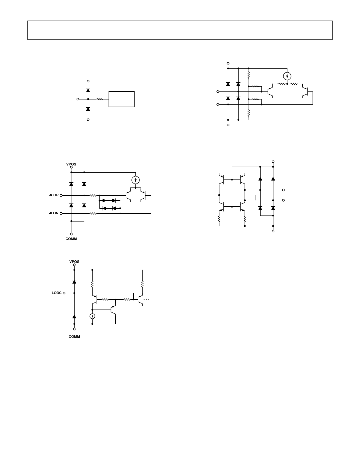
EQUIVALENT INPUT CIRCUITS
VPOS
VPOS
PHxx
ENBL
RSET
COMM
Figure 3. Logic Inputs
Figure 4. Local Oscillator Inputs
LOGIC
INTERFACE
RFxP
RFxN
COMM
Figure 6. RF Inpu ts
COMM
VNEG
Figure 7. Output Drivers
IxNO
QxNO
IxPO
QxPO
Figure 5. LO Decoupling Pin
Rev. PrB Page 7 of 29
Page 8

AD8339 Preliminary Technical Data
TYPICAL PERFORMANCE CHARACTERISTICS
VS = ±5 V, TA = 25°C, 4fLO = 20 MHz, fLO = 5 MHz, fRF= 5.01 MHz, fBB = 10 kHz, P
performance, differential voltages, dBm (50), phase select code = 0000, unless otherwise noted (see default test circuit).
≥ 0 dBm (50); single-ended sine wave; per channel
LO
Rev. PrB Page 8 of 29
Page 9

AD8339 Preliminary Technical Data
TEST CIRCUITS
Rev. PrB Page 9 of 29
Page 10

Preliminary Technical Data AD8339
THEORY OF OPERATION
RF2N
RF2P
COMM
COMM
SCLK
CSB
VPOS
VPOS
RF3P
RF3N
1
2
3
4
5
6
7
8
9
10
40
SERIAL
INTERFACE
(SPI)
90
BIAS
AD8339
39
0
38 37
36
0
V TO I
V TO I
0
LOCAL OSCILLATOR DIVIDE BY 4
90
V TO I
V TO I
34
35 33
32
CURRENT
MIRROR
CURRENT
MIRROR
CURRENT
MIRROR
CURRENT
MIRROR
CURRENT
MIRROR
CURRENT
MIRROR
CURRENT
MIRROR
CURRENT
MIRROR
31
30
Q2OP
29
I2OP
28
VPOS
27
VPOS
4LOP
26
25
4LON
24
VNEG
23
VNEG
22
I3OP
21
Q3OP
11 13 14
Figure 8. AD8339 Block Diagram
The AD8339 is a quad I/Q demodulator with a programmable
phase shifter for each channel. The primary application is
phased array beamforming in medical ultrasound. Other
potential applications might be phased array radar, and smart
antennas for mobile communications. The AD8339 can also be
used in applications that require multiple well-matched I/Q
demodulators. The AD8339 is architecturally very similar to its
predecessor – the AD8333. The major differences are:
1. the addition of a serial (SPI) interface that allows daisychaining of multiple devices
2. reduced power per channel at the expense of a slight
decrease in dynamic range
Figure 8 shows the block diagram and pinout of the AD8339.
Four RF inputs accept signals from the RF sources, and a local
oscillator (applied to differential input pins marked 4LOP and 4
LON) common to all channels, comprise the analog inputs.
Rev. PrB Page 10 of 29
15
16 19 2012 17 18
Each channel has the option to program 16 delay states/360° (or
22.5°/step) selectable via the SPI port. The part has two reset
inputs: RSET is used to synchronize the LO dividers in multiple
AD8339s used in arrays; RSTS is used to set the SPI port bits to
all zeros. This can be useful in testing or when one quickly
wants to turn off the device without first programming the SPI
port.
Each of the current formatted I and Q outputs sum together for
beamforming applications. Multiple channels are summed and
converted to a voltage using a transimpedance amplifier. If
desired, channels can also be used individually.
QUADRATURE GENERATION
The internal 0° and 90° LO phases are digitally generated by a
divide-by-four logic circuit. The divider is dc-coupled and
inherently broadband; the maximum LO frequency is limited
only by its switching speed. The duty cycle of the quadrature LO
Page 11

AD8339 Preliminary Technical Data
signals is intrinsically 50% and is unaffected by the asymmetry
of the externally connected 4×LO input. Furthermore, the
divider is implemented such that the 4×LO signal re-clocks the
final flip-flops that generate the internal LO signals and thereby
minimizes noise introduced by the divide circuitry.
For optimum performance, the 4xLO input is driven
differentially, but can also be driven single-ended. A good
choice for a drive is an LVDS device. The common-mode range
on each pin is approximately 0.2 V to 3.8 V with the nominal
±5 V supplies.
The minimum 4×LO level is frequency dependent. For
optimum noise performance it is important to ensure that the
LO source has very low phase noise (jitter) and adequate input
level to assure stable mixer-core switching. The gain through
the divider determines the LO signal level vs. RF frequency. The
AD8339 can be operated to very low frequencies at the LO
inputs if a square wave is used to drive the LO.
Beamforming applications require a precise channel-to-channel
phase relationship for coherence among multiple channels. A
reset pin is provided to synchronize the LO divider circuits in
different AD8339s when they are used in arrays. The RSET pin
resets the dividers to a known state after power is applied to
multiple AD8339s. A logic input must be provided to the RSET
pin when using more than one AD8339. Note that at least one
channel must be enabled for the LO interface to also be enabled
and the LO reset to work. See the Reset Input section in the
applications section for more detail.
I/Q DEMODULATOR AND PHASE SHIFTER
The I/Q demodulators consist of double-balanced Gilbert cell
mixers. The RF input signals are converted into currents by
transconductance stages that have a maximum differential input
signal capability of 2.7 V p-p. These currents are then presented to
the mixers, which convert them to baseband: RF − LO and
RF + LO. The signals are phase shifted according to the codes
programmed into the SPI latch (see Table 4); the phase bits are
labeled PHx0 through PHx3 where ‘0’ indicates LSB and ‘3’
indicates MSB. The phase shift function is an integral part of the
overall circuit (patent pending). The phase shift listed in Column 1
of Table 4 is defined as being between the baseband I or Q channel
outputs. As an example, for a common signal applied to a pair of
RF-inputs to an AD8339, the baseband outputs are in phase for
matching phase codes. However, if the phase code for Channel 1 is
0000 and that of Channel 2 is 0001, then Channel 2 leads Channel 1
by 22.5°.
Following the phase shift circuitry, the differential current
signal is converted from differential to single-ended via a
current mirror. An external transimpedance amplifier is needed
to convert the I and Q outputs to voltages.
Rev PrB Page 11 of 29
Table 4. Phase Select Code for Channel-to-Channel Phase
Shift
φ-Shift
0º
22.5º
45º
67.5º
90º
112.5º
135º
157.5º
180º
202.5º
225º
247.5º
270º
292.5º
315º
337.5º
PHx3 (MSB) PHx2 PHx1 PHx0 (LSB)
0
0
0
0
0
0
0
0
1
1
1
1
1
1
1
1
0
0
0
0
1
1
1
1
0
0
0
0
1
1
1
1
0
0
1
1
0
0
1
1
0
0
1
1
0
0
1
1
0
1
0
1
0
1
0
1
0
1
0
1
0
1
0
1
DYNAMIC RANGE AND NOISE
Figure 9 is an interconnection block diagram of two channels
(1/2 of the AD8339), more channels are easily added to the
summation (up to 16 when using an AD8021 as the summation
amplifier) by wire-or connecting the outputs as shown for two
channels. For optimum system noise performance, the RF
input signal is provided by a very low noise amplifier such as
the LNA of the AD8332/AD8334 or the preamplifier of the
AD8335. In beamformer applications, the I and Q outputs of a
number of receiver channels are summed (for example, the two
channels illustrated in Figure 9). The dynamic range of the
system increases by the factor 10log
number of channels (assuming random uncorrelated noise.)
The noise in the two channel example of Figure 9 is increased
by 3 dB while the signal doubles (+6 dB), yielding an aggregate
SNR improvement of (+6 − 3) = +3 dB. For four channels the
dynamic range will increase by +6 dB and so on.
Judicious selection of the RF amplifier ensures the least
degradation in dynamic range. The input referred spectral
voltage noise density (e
nV/√Hz. For the noise of the AD8339 to degrade the
TBD
) of the AD8339 is nominally about
n
system noise figure (NF) by 1 dB, the combined noise of the
source and the LNA should be about twice that of the AD8339
nV/√Hz. If the noise of the circuitry before the AD8339
or TBD
is less than TBD
nV/√Hz then the system NF degrades more
than 1 dB. For example, if the noise contribution of the LNA
and source is equal to the AD8339, or TBD
degradation is 3 dB. If the circuit noise preceding the AD8339 is
1.3× as large as that of the AD8339 (or about TBD nV/√Hz) the
degradation is 2 dB. For a circuit noise 1.45× that of the
AD8339 (TBD
nV/√Hz) the degradation is 1.5 dB.
To determine the input referred noise it is important to know the
active low pass filter (LPF) values R
Typical filter values for a single channel are 1.58 kΩ and 1 nF, and
implement a 100 kHz single-pole LPF. In the case that two channels
are summed as is done on the evaluation board, the values would
(N), where N is the
10
nV/√Hz, the
FILT
and C
, shown in Figure 9.
FILT
Page 12

Preliminary Technical Data AD8339
be the same as for a single channel of the AD8333, namely 787 Ω
and 2.2 nF.
If the RF and LO are offset by 10 kHz, the demodulated signal is 10
kHz and is passed by the LPF. The single-channel mixing gain,
from the RF input to the AD8021 output (for example, I1´, Q1´) is
approximately 1.7 (4.7 dB). This together with the TBD
AD8339 noise results in about TBD
output. Since the AD8021, including the 1.58 kΩ feedback resistor,
contributes another 6.3 nV/√Hz, the total output referred noise is
nV/√Hz at the AD8021
nV/√Hz of
about TBD
filter resistor while maintaining the corner frequency, thereby
increasing the gain. The factor limiting the magnitude of the gain is
the output swing and drive capability of the op-amp selected for the
I-to-V converter, in this instance the AD8021.
Because any amplifier has limited drive capability there will be a
finite number of channels that can be summed. This is explained in
great detail in the section below called – Channel Summing.
nV/√Hz. This value can be adjusted by increasing the
Figure 9. Interconnection Block Diagram for ½ of AD8339
SUMMATION OF MULTIPLE CHANNELS (ANALOG
BEAMFORMING)
Beamforming, as applied to medical ultrasound, is defined as the
phase alignment and summation of signals generated from a
common source, but received at different times by a multielement ultrasound transducer. Beamforming has two functions:
it imparts directivity to the transducer, enhancing its gain and it
defines a focal point within the body from which the location of
the returning echo is derived. The primary application for the
AD8339 is in analog beamforming circuits for ultrasound.
PHASE COMPENSATION AND ANALOG
BEAMFORMING
Modern ultrasound machines used for medical applications
employ an array of receivers for beamforming, with typical CW
Rev. PrB Page 12 of 29
Doppler array sizes up to 64 receiver channels phase-shifted
and summed together to extract coherent information. When
used in multiples, the desired signals from each of the channels
can be summed to yield a larger signal (increased by a factor N,
where N is the number of channels), while the noise is
increased by the square root of the number of channels. This
technique enhances the signal to noise performance of the
machine. The critical elements in a beamformer design are the
means to align the incoming signals in the time domain, and
the means to sum the individual signals into a composite whole.
In traditional analog beamformers incorporating Doppler, a
V-to-I converter per channel and a cross-point switch precede
passive delay lines used as a combined phase shifter and
summing circuit. The system operates at the receive frequency
(RF) through the delay line which also sums the signals from
Page 13

AD8339 Preliminary Technical Data
the various channels, and then the combined signal is downconverted by a very large dynamic range I/Q demodulator.
The resultant I and Q signals are filtered and then sampled by
two high resolution AD converters. The sampled signals are
processed to extract the relevant Doppler information.
Alternatively, the RF signal can be processed by downconversion on each channel individually, phase shifting the
down-converted signal, and then combining all channels. The
AD8333 and the AD8339 provide the means to implement this
architecture. The down-conversion is done by an I/Q
demodulator on each channel, and the summed current output
is the same as in the delay line approach. The subsequent filters
after the I-to-V conversion and the AD converters are similar.
The AD8339 integrates the phase shifter, frequency conversion,
and I/Q demodulation into a single package, and directly yields
the baseband signal.
Figure 10 is a simplified diagram showing the idea for two
channels. The ultrasound wave USW is received by two
transducer elements, TE1 and TE2, in an ultrasound probe and
generates signals E1 and E2. In this example, the phase at TE1
leads the phase at TE2 by 45°.
Figure 10. Simplified Example of the AD8339 Phase Shifter
In a real application, the phase difference depends on the
element spacing, λ (wavelength), speed of sound, angle of
incidence, and other factors. The signals ES1 and ES2 are
amplified 19 dB by the low-noise amplifiers in the AD8332; for
lower performance portable ultrasound applications, the
combination of the AD8335 and the AD8339 result in the
lowest power per channel. For optimum signal-to-noise
performance, the output of the LNA is applied directly to the
input of the AD8339. In order to sum the signals ES1 and ES2,
ES2 is shifted 45° relative to ES1 by setting the phase code in
Channel 2 to 0010. The phase aligned current signals at the
output of the AD8333 are summed in an I-to-V converter to
provide the combined output signal with a theoretical
improvement in dynamic range of 3 dB for the sum of two
channels.
SERIAL INTERFACE
The AD8339 contains a 4-wire SPI compatible digital interface
(SDI, SCLK, CSB, and SDO). The interface is comprised of a 20bit shift register plus a latch. The shift register needs to be loaded
MSB first. The data allows control over each channel’s phases,
plus the last four bits shifted into the register determine the
enable state of the individual channels. Figure 11 shows a block
Rev PrB Page 13 of 29
diagram of the serial interface, and Figure 12 its timing
diagram. The shift direction is to the “right” with MSB first. As
soon as CSB goes low, the data is latched and new data can be
loaded into the shift register.
20 bits are required to program each AD8339 and the data is
latched when CSB goes high. Depending on the data, the
corresponding channels are enabled, and the phases are
selected. Figure 12 illustrates the timing for two sequentially
programmed devices.
ENBL Bits
If all four ENBL bits are set to ‘0’, then only the SPI port is
powered up. This feature allows for very low power
consumption (about 13 mW per AD8339 or 3.25 mW per
channel) when the CW Doppler function is not needed. Since
the SPI port stays alive even when the rest of the chip is
powered down, the part can be awakened again by simply
programming the port. As soon as the CSB signal goes high, the
part turns on again. It should be pointed out that this will take a
fair amount of time because of the external capacitor on the
LODC pin. It will take about 10-20 μs with the recommended
0.1 μF decoupling cap. The decoupling cap on this pin is
intended to reduce bias noise contribution in the LO divider
Page 14

Preliminary Technical Data AD8339
chain. The user can experiment with the value of this
decoupling capacitor to see what the smallest value can be
without any dynamic range degradation within the frequency
band of interest.
The SPI also has an additional pin that can be used in a test
mode, or as a quick way to reset the SPI and de-power the chip.
All bits in both the shift register and the latch can be reset to ‘0’
Figure 11. Serial Interface Showing the 20 Bit shift Register and Latch
when pin RSTS is pulled above about 1.2 V. For quick testing
without the need to program the SPI, the voltage on the RSTS
pin should be first pulled high and then pulled to -1.4 V; this
enables all four channels in the (I=1,Q=0) state (all phase bits
are 0000).
C43
C40
C33
C41
C42
C32
C23
C22
C30
C31
C21
C12
C11
C13
C20
C10
EN3
C43
C40
C33
C41
C42
EN1
EN0
EN2
C43
C42
C41
C40
C33
C32
C32
C31
C31
C30
C30
C23
C23
C22
C22
C21
C21
C20
C20
C13
C13
C12
C12
C11
C11
C10
C10
EN3
EN3
EN2
EN2
EN1
EN1
EN0
EN0
C43
C42
Figure 12. Timing Diagram
Rev. PrB Page 14 of 29
Page 15

AD8339 Preliminary Technical Data
APPLICATIONS
The AD8339 is the key component of a phase-shifter system
that aligns time-skewed information contained in RF signals.
Combined with a variable gain amplifier (VGA) and low noise
amplifier (LNA) as in the AD8334/5 VGA family, the AD8339
forms a complete analog receiver for a high-performance
ultrasound system.
LOGIC INPUTS AND INTERFACES
All logic inputs of the AD8339 including the SPI and RSET pins
are CMOS compatible down to 1.8 V. Each logic input pin has a
Schmitt trigger activated input that contains a threshold that is
centered at about 1.1 V with a hysteresis of ±0.1 V around this
value.
The LO divider RSET pin has a slightly higher threshold at
about 1.3 V and a hysteresis of about ±0.1 V. This input also can
still be driven by 1.8 V CMOS logic.
The only logic output, SDO, generates a signal that has a logic
low level of about 0.2 V and a logic high level of about 1.9V to
allow for easy interfacing to the next AD8339 SDI input.
RESET INPUT
The RSET pin is used to synchronize the LO dividers in
AD8339 arrays. Because they are driven by the same internal
LO, the four channels in any AD8339 are inherently
synchronous. However, when multiple AD8339s are used it is
possible that their dividers wake up in different phase states.
The function of the RSET pin is to phase align all the LO signals
in multiple AD8339s.
The 4 × LO divider of each AD8339 can initiate in one of four
possible states - 0°, 90°, 180°, and 270° relative to other
AD8339s. The internally generated I/Q signals of each AD8339
LO are always at a 90° angle relative to each other, but a phase
shift can occur during power up between the internal local
oscillators of multiple AD8339s used in a common array.
The LO divider reset function has been improved in the
AD8339 over the AD8333. The RSET pin still provides an
asynchronous reset of the LO dividers by forcing the internal
LO to "hang", however, now the LO reset function is fast and
does not require a shutdown of the 4 x LO input signal.
The RSET mechanism also allows the measurement of nonmixing gain from the RF input to the output.
The rising edge of the active high RSET pulse can occur at any
time; however, the duration should be ≥ 20 ns minimum. When
the RSET pulse transitions from high to low, the LO dividers are
reactivated on the next rising edge of the 4 x LO clock. To
guarantee synchronous operation of an array of AD8339s the
RSET pulse needs to go low on all devices before the next rising
edge of the 4 x LO clock. Therefore it is best to have the RSET
pulse go low on the falling edge of the 4 x LO clock; at the very
least the t
would be for the RSET pulse to go high on a 4 x LO falling edge
should be ≥ 5 ns. An optimal timing set-up
SET-UP
and go low on a 4×LO falling edge; this gives 10 ns of set-up
time even at a 4×LO frequency of 50 MHz (12.5 MHz internal
LO).
Check the synchronization of multiple AD8339s using the
following procedure:
1. Activate at least one channel per AD8339 by setting
the appropriate channel enable bit in the serial
interface.
2. Set the phase code of all AD8339 channels the same,
for example, 0000.
3. Apply the same test signal to all devices that generates
a sine wave in the baseband output and measure the
output of one channel per device.
4. Apply a RSET pulse to all AD8339s.
5. Since all the phase codes of the AD8339s should be
the same, the combined signal of multiple devices
should be N times bigger than a single channel. If the
combined signal is less than N times one channel,
then the LO phases of the individual AD8339s are
most likely in error.
Rev PrB Page 15 of 29
Page 16

Preliminary Technical Data AD8339
EVALUATION BOARD
Figure 13 is a photo of the AD8339 evaluation board, and the
schematic diagram is shown in Figure 18, Figure 19 and
Figure 20. Four single-ended rf inputs may be phase aligned
using the LNA inputs of an AD8334, and the 16 phase
adjustment options the AD8339. The rf input signals may be
derived from three sources, user selectable by jumpers. Test
points enable signal tracing at various circuit nodes. The
AD8339 requires dual power supplies, the AD8334 and digital
section only a single supply. A 3.3V on-board regulator provides
power for the USB and EEPROM devices. The AD8339 may be
configured using the software provided on the CD-ROM
included with the board, or using an external digital pattern
generator via the 20-pin flat-cable connector.
Figure 13. AD8339 Evaluation Board
CONNECTIONS TO THE BOARD
Table 5 is a list of equipment required to activate the board with
suggested test equipment, and Figure 16 shows a typical setup.
In order to phase align any two rf input signals, the rf and clock
inputs must be coherent, i.e., from the same timing source.
Many laboratory signal generators have this capability,
including the Rohde and Schwartz model shown in the table.
Rev. PrB Page 16 of 29
Other signal generators may also used; the only requirement is
that they have external clock inputs and outputs. Selecting the
frequency of the generators is quite simple. As an example,
select an rf frequency of interest, for example 5 MHz. Then
select the 4LO frequency, which is four times the rf frequency,
in this example 20 MHz. The output frequency is 0 Hz – note
that the eval-board cannot provide a dc component. To detect
Page 17

AD8339 Preliminary Technical Data
an output, advance or retard the rf frequency by the desired
baseband frequency. A baseband frequency of 10 kHz at the
output will result from an rf frequency of 5.01MHz.
Table 5. Recommended Equipment List
Description Suggested Equipment
Signal Generators (2), with synchronizing connectors. Rohde and Schwartz, SMT3 or equivalent
4 Channel Oscilloscope, Tektronix DPO7104, or equivalent
Power Supplies Agilent E3631A or Equivalent
Scope Probes (4) Tektronix P6104 or Equivalent
TEST CONFIGURATIONS
The three test configuration options for the AD8339-EVALZ
are common input, independent input and AD9271 drive.
Common Input Signal Drive
Figure 14 is a block diagram showing the simplest way to use
the eval board, with a common signal applied to all four
AD8339 inputs in parallel. Boards are configured this way as
shipped. The inputs of each of the channels are connected in
common by means of jumpers as shown in the Table 4,
although they can be just as easily connected to any of the
AD8334 LNA outputs. Figure 14 is a block diagram of the
connection. As seen in Figure 19, two pairs of summing
amplifiers provide the I and Q outputs so channels 1 and 2 can
be observed, independently of channels 3 and 4.
Using a common input signal source as shown in Figure 16, the
same input is applied to all four channels of the AD8339. To
observe an output at the I or Q connectors, simply enable the
appropriate channel or channels using the menu shown in
Figure 17. For example if channels 1 is enabled and the phases
set to 0°, a waveform will be seen at the I1+I2 and Q1+Q2
outputs. If channel 2 is enabled, with the phase also set to 0°,
the amplitude of the waveforms will double. If channel 1 is 0°
and channel 2 phase set to 180°, the output will become zero
because the phases of the two channels will cancel.
When using the common input drive mode it is important that
only the top two positions of P4A and P4B are used in order to
avoid shorting the LNA outputs together.
Independent Channel Drive
Independent input mode simply means that each channel is
driven by an LNA. Of course the LNA inputs of the AD8334
may be driven by up to 4 independent signal generators, or
from a single generator. If the user opts for this mode, it is
important to not connect the LNA inputs in parallel, because of
the active matching feature. Any standard splitter may be used.
AD9271 Input Drive
Connectors P3A, P3B and P$A, P4B are configured to route
input signals from the AD8334 LNA outputs, or from an
AD9271 eval board. When using an AD9271 as an input drive,
consult the AD9271 data sheet for setup details.
The AD9271 board is attached to the AD8339 by inserting the
three plastic stand-offs into the three guide holes in the
AD8339-EVALZ board; all the jumpers in P3 and P4 are
removed. The bottom connectors of the AD9271 board will
engage P3 and P4 and route the LNA outputs of the AD9271 to
the AD8339. Figure 15 is a photo of the two boards attached.
Table 6. P3, P4 Input Jumper Configuration
Common Input Independent AD9271 Input
Input
P4A-1 to P4B-1, P3A-1 to P3B-1
Top 2 positions (2) P4A-1 to P4B-1
RF12N, RF12P, P3A-1 to P3B-1,
RF23N, RF23P, P4A-1 to P4B-1,
RF34N, RF34P all positions (8)
Rev PrB Page 17 of 29
Page 18

Preliminary Technical Data AD8339
COMMON
SIGNAL
PATH
AD8334
LNA
AD8339
CH1
RF
CH2
RF
CH3
RF
CH4
RF
Figure 14. AD8339 Test Configuration – Common Signal Input Drive
I1
Q1
I2
Q2
I3
Q3
I4
Q4
Q1 + Q2
I TO V
I1 + I2
I TO V
I TO V
I3 + I4
Q3 + Q4
I TO V
Figure 15. AD8339-EVALZ with AD9271 Attached as Input Source
Rev. PrB Page 18 of 29
Page 19

AD8339 Preliminary Technical Data
TOP:
SIGNAL GENERATOR FOR 4LO INPUT e.g. 20MHz, 1V
BOTTOM:
SIGNAL GENERATOR FOR RF INPUT e.g. 5.01 MHz
P-P
SYNCHRONIZE
GENERATORS
POWER
SPLITTER
USB
CABLE
PERSONAL
COMPUTER
+5 V
POWER SUPPLY
-5 V
4LO
INPUT
Figure 16. AD8339-EVALZ Typical Test Setup
Using the SPI Port
Channel and phase selection are accessed via the SPI port on
the AD8339 and the eval board provides two means of access. If
it is desired to exercise the SPI input with custom waveforms,
the SDI, SCLK and CSB are available at the auxiliary connector
P1. A digital pattern generator may be programmed in
Rev PrB Page 19 of 29
OUTPUTS
conformance with the timing diagram as shown in Figure 12.
The most convenient way to select channels and phase delays is
the executable program provided on the CD ROM or ADI
website. Copy the .EXE and .MSI files into the same folder on
the PC. Double-click on the ‘.EXE’ file and the program will
self-install and place a short cut on the desktop. Double-clicking
Page 20

Preliminary Technical Data AD8339
on the desktop icon will bring up the control menu, as shown in clicking on the boxes in the list, and the 16 phase options are
Figure 17. The menu consists of an array of radio buttons,
which are self-explanatory. Channels are enabled or disabled by
Figure 17. SPI Software Control Menu
selected from a drop-down menu for each of the channels.
Hard-wired Jumpers
Hard-wired jumpers provide for interconnection of channels
and as a means for measuring output voltages at various
strategic modes.
When shipped, the board is configured so as to connect all the
AD8339 rf inputs to a single LNA output. In this configuration,
Table 7. Jumper and Header List
Jumper, Header Description
AxSHT Shorts the Current Summing Outputs – Shipped Omitted
CSB Connects the Chip Select Input to the Connector or the USB Inputs – Normally Connected to USB (Test)
CSBG Grounds the CSB Input – Shipped Omitted
EN12, EN34 Enables or Disables Channels 1 through 4 – Boards Shipped Enabled
G12, G34 Connects Gain Pin for Channels 1 through 4 to Ground - Boards are Shipped with these Jumpers Inserted
I1234 Sums All Four I Channel Current Outputs Together – Shipped Omitted
Q1234 Sums All Four Q Channel Current Outputs Together – Shipped Omitted
RF1 Through RF4 Test Points for the LNA Outputs – A Differential Probe Will Fit These
RSTS Resets the SPI Input – Shipped Omitted
RSET Resets the Local Oscillator Inpyt – Shipped Omitted
SDIG Grounds the SDI Input
SCLK Connects the S-Clock Input to the Connector or the USB Inputs – Normally Connected to the USB (Test)
SDI Connects the Serial Data Input to the Connector or the USB Input – Normally Connected to the USB (Test)
SLKG Grounds the S-Clock Input – Shipped Omitted
VO1 Through VO4 Test Points for the VGA Outputs – A Differential Probe Will Fit These
4LO Test Pins for the 4LO Level Shifter Output – A Differential probe Will fit These
the phases of the four channels can be shifted throughout the
full range and the outputs viewed on a multichannel scope
using one of the channels as a reference. To operate all the LNA
channels independently it is only necessary to move the input
shorting jumpers to the channel rf outputs.
Rev. PrB Page 20 of 29
Page 21

AD8339 Preliminary Technical Data
LOP1 LON1
IN2
LON2
LOP2
LOP3
LON3
C61
0.1
120nH
IN3
L7
120nH
5V
F
L8
IN2S
RF2
RF3
IN3S
CFB2
18nF
RFB2
274Ω
R44
20Ω
R43
20Ω
L16
120nH
L17
120nH
C46
0.1 F
R46
20Ω
R45
20Ω
RFB3
274Ω
CFB3
18nF
0.1 F
C10
22pF
C88
IN1
C60
0.1
C8
22pF
C43
0.1 F
C44
0.1 F
0.1 F
C87
0.1 F
C47
0.1 F
C48
0.1
IN4
F
C45
F
L10
120nH
IN1S
1
2
3
4
7
8
9
10
11
12
13
14
15
16
L9
120nH
5
6
INH2
LMD2
COM2X
LON2
LOP2
VIP2
VIN2
VPS2
VPS3
VIN3
VIP3
LOP3
LON3
COM3X
LMD3
INH3
IN4S
0.1
64
COM2
COM3
17
C67
F
C6
22pF
63
COM1
PIN 1
IDENTIFIER
COM4
18
C62
0.1 F
C12
22pF
62
INH1
INH4
19
CFB1
18nF
C68
0.1 F
CFB4
18nF
61
20
LMD1
LMD4
RFB1
274Ω
C55
0.1 F
RFB4
274Ω
60
COM1X
COM4X
21
R47
20Ω
R50
20Ω
59
LON1
LON4
22
RF4
58
23
0.1
LOP1
LOP4
0.1
RF1
C54
C49
R48
20Ω
R49
20Ω
C53
0.1 F
F
57
VIP1
U1
AD8334
VIP4
24
F
C50
0.1 F
120nH
5V
F
52
29
EN
EN12 EN34
51
EN12
EN34
HILO
VCM4
30
C56
0.1 F
L13
120nH
C86
F
0.1
C66
0.1
R??
0Ω
53
54
55
56
VIN1
VPS1
GAIN12
CLMP12
VIN4
VPS4
26
25
R64
0Ω
L12
GAIN34
27
C63
0.1 F
C85
0.1 F
CLMP34
28
C58
0.1 F
50
31
VCM1
VCM3
C57
0.1 F
EN
DISDIS
VCM2
COM12
COM12
COM34
VPS34
COM34
5V
C59
0.1
49
VOH1
VOL1
VPS12
VOL2
VOH2
MODE
NC
VOH3
VOL3
VOL4
VOH4
NC
32
F
48
47
NC
46
NC
45
44
NC
43
NC
42
41
40
39
38
NC
37
36
35
NC
34
NC
33
120 nH
C65
0.1 F
C64
0.1 F
L14
L15
120 nH
5V
5V
5V
LON4 LOP4
Figure 18. Schematic - LNA Section
Rev PrB Page 21 of 29
Page 22

Preliminary Technical Data AD8339
R35
5.23kΩ
R29
4.22kΩ
R68
5.23kΩ
RF2N
RF2P
R66
4.22kΩ
5V
R67
5.23kΩ
VPOS
RF3P
RF3N
R65
4.22kΩ
RF1P
5V
R31
2.8kΩ
R32
2.8kΩ
5V
RF12N RF12P
R60
0Ω
R71
2.8kΩ
R59
0Ω
R72
2.8kΩ
RF23P
R58
0Ω
R69
2.8kΩ
R70
2.8kΩ
R57
0Ω
VPOS
RF1N
W12
W13
N12
P12
R1
1kΩ
R3
1kΩ
CSB
CSBG
SLKG
SDI
RSTS
CSB
(SHT3)
SCLK
SCLK
(SHT3)
W4
W2
W1
SDI
(SHT3)
RF1P RF1N
R61
0Ω
403839
RSTS
VPOS
11
SDI
PIN 1
IDENTIFIER
SDO
12
1
RF2N
2
RF2P
3
COMM
4
COMM
5
SLKG
RF23N
SCLK
CSBG
6
CSB
C16
0.1 F VNEG
7
VPOS
8
VPOS
9
RF3P
10
RF3N Q3OP
RF34P
RF1P
RF4P
13
37
RF1N
RF4N
14
RF34N
0.1
RF2P
C17
SDO
F
RF2N
W10
W11
P23
SDO
SDO
RF3P
N23
W9
5V
R56
0Ω
RF3N
P34
W8
R34
2.8kΩ
W6
N34
R4
1kΩ
R62
0Ω
R51
0Ω
0.1
R33
2.8kΩ
W7
5V
VPIS
VPOS
C1
F
36
35
VPOS
COMM
DUT
AD8339
COMM
VPOS
15
16
VPOS
P1
12
4
3
6
5
8
10
12
14
16
18
20
L2
RSET
7
9
11
13
15
17
19
5V
120nH
VNIS
SDO
120nH
C31
0.1 F
VNEG
34
33
32
31
I1OP
RSET
LODC
17
C19
0.1
C18
0.1
R36
5.23kΩ
R30
4.22kΩ
COMPONENTS SHOWN IN
Q1OP
VNEG
I4OP
Q4OP
VNEG
F
F
5V
VNEG
GRAY ARE NOT
INSTALLED
Q2OP
I2OP
VPOS
VPOS
4LOP
4LON
VNEG
VNEG
I3OP
R6
0Ω
R5
0Ω
L1
C27
0.1 F
C20
0.1
30
29
VPOS
28
27
26
25
24
23
22
21
-5V
R21
0Ω
R20
0Ω
R19
0Ω
R18
0Ω
4LO
R8
0Ω
R7
0Ω
Q4OP
F
Q1OP
C30
0.1 F
C29
0.1 F
I4OP
I1OP
VA
R15
0Ω
VA
R12
0Ω
I1234 Q1234
DSC90C401
R27
100Ω
VA
R9
0Ω
R2
0Ω
U7
VA
C24
0.1 F
3
2
2 7
-
1
AD8021
8
+
3
4
2 7
-
1
AD8021
8
+
3
4
2 7
-
1
AD8021
8
+
3
4
2 7
-
U6
1
AD8021
8
+
3
4
C26
0.1
VPOS
4
C22
0.1 F
C52
0.1
C25
0.1
5
C84
5PF
F
C23
0.1 F
5
C82
5PF
R28
3.48kΩ
R37
1.5kΩ
C21
0.1 F
5
C80
5PF
C51
0.1
5
C33
5PF
F
R16
787
C83
2.2nF
F
R17
6
0
Q1+Q2
-VA
R13
787
C81
2.2nF
R14
6
0
I1+I2
-VA
C28
0.1 F
R10
787
C79
2.2nF
R11
6
49.9Ω
0
LOP
R54
I3+I4
-VA
R42
787
C32
F
2.2nF
R38
Q3+Q4
6
0
-VA
P4A
P4B
5V
22
1
1
FROM AD9271
1
P3A
1
P3B
C34
0.1 F
8
U7
DSC90C401
1
7
6
LOP1
LON1
LOP2
LON2
LOP3
LON3
LOP4
LON4
5
Rev. PrB Page 22 of 29
Page 23

AD8339 Preliminary Technical Data
Figure 19. Schematic - IQ Demodulator and Phase Shifter
Rev PrB Page 23 of 29
Page 24

Preliminary Technical Data AD8339
5VS -5VS VAS -VAS
RED ORG GRN BLUE
PLUS
C13
10 F
+
25V
L6
120nH
C37
0.1 F
L5
5V
NC NC
GND
PD7/FD15
PD6/FD14
CY7C68013A-56LFXC
PB0/FD0
NC
C73
0.1
PB2/FD2
PB1/FD1
20
NC
NC
F
-5V
50 4956 55 51 54 53 52
NC
MINUS
+
C11
10 F
25V
L4
120nH
C36
0.1 F
0.1 F
VA
NC NC
48 47 4346 45 44
PD5/FD13
PD4/FD12
PD3/FD11
U2
PB3/FD3
PB4/FD4
PB5/FD5
23
NC
NC
NC
R22
R23
R24
R25
R26
C15
10 F
25V
120nH
C35
NC
2415 16
+
L15
PD2/FD10
PB6/FD6
NC
R41
-VA
100k
NC
NC
PD1/FD9
PD0/FD8
PA7/FLAGD/SLCS
GND
PB7/FD7
25 26 27
NC
GND1 GND4 GND3 GND2
-VAS
VAS
-5VS
5VS
3.3V
C5
22pF
VCC
WAKEUP
RESET#
PA6/PKTEND
PA5/FIFOADR1
PA4/FIFOADR0
PA3/WU2
PA2/SLOE
PA1/INT1#
PA0/INT0#
CTL2/FLAGC
CTL1/FLAGB
CTL0/FLAGA
GND
VCC
28
C74
0.1
3.3V
GND
VCC
F
C76
0.1 F
42
41
40
39
38
37
36
35
34
33
32
31
30
29
NC
NC
NC
NC
NC
NC
NC
NC
3.3V
R40
100k
C4
22pF
CSB(SHT2)
SCLK(SHT2)
SDI (SHT2)
3.3V
C75
0.1 F
GND6 GND5 GND7 GND8
BLK
TEST
LOOP
(8)
C78
0.1 F
A7
USB TYPE B
GND
5V
W3
3 12
IN
C3
12 pF
D+
23
4
1
24LC00/P
VBUS
Z1
OUT
OUT
TAB
Y1
24MHz
D-
C9
1 F
10V
+
GND
ADP3339AKC-3.3
3.3V
C69
0.1 F
C2
12 pF
3.3V
C70
0.1 F
5V
555
3.3V
499
C71
0.1 F
CR1
R39
10k
C72
0.1
F
A0
A1
A2
VSS
VCC
WP
SCL
SDA
8
7
6
5
1
2
3
4
L11
120 nH
A6
1
NC
RDY0/SLRD
2
RDY1/SLWR
NC
3
AVCC
4
XTALOUT
5
XTALIN
6
GND
7
AVCC
8
DPLUS
9
DMINUS
10
GND
11
VCC
12
GND
13
IFCLK/PE0/TOUT
NC
14
RESERVED
3.3V
22.1k
R53
22.1k
R52
C77
0.1 F
GND
+
C14
10 F
25V
120nH
C38
0.1 F
3.3V
C7
0.1
F
NC
VCC
CLKOUT/PE1/T1OUT
SDA
SCL
VCC
17 18 19 21 22
3.3V
Figure 20. Schematic – USB
Rev. PrB Page 24 of 29
Page 25

AD8339 Preliminary Technical Data
AD8339-EVALZ ARTWORK
Figures xxx, are the artwork for the Ad8339-EVALZ
Figure 21. AD8339-EVALZ Component Side Copper
Figure 22. AD8339-EVALZ Wiring Side Copper
Rev PrB Page 25 of 29
Page 26

Preliminary Technical Data AD8339
Figure 23. AD8339-EVALZ Component Side Silkscreen
Figure 24. AD8339-EVALZ Assembly
Rev. PrB Page 26 of 29
Page 27

AD8339 Preliminary Technical Data
Qt y Name Description Reference Designator Manufacturer Mfg. Part
Number
1 Test Loop Green −5VS Components Corp. TP-104-01-05
1 Test Loop Blue −VAS Components Corp. TP-104-01-06
24
Header
1
Test Loop
1
Integrated
Circuit
1
Connector
63
Capacitor
2
Capacitor
6
Capacitor
1
Capacitor
4
Capacitor
4
Capacitor
4
Capacitor
4
Capacitor
1
LED
13
Test Loop
1
Integrated
Circuit
7
Header
9
Test Loop
9
Connector
17
Bead
1
Connector
3
Connector
2
Connector
2
Connector
3
Resistor
31
Resistor
4
Resistor
BERG 2
Red
3.3V REGULATOR
Rt Angle USB, Type B, 4
Pos
0.1 µF, 16 V, 0603 X7R
12pF 50V 5% 0603
22pF 50V 5% 0603
1 µF, 6.3 V 10% 0603
Tantalum 10 µF, 10 V,
20%, 3216 SMD
2.2nF 50V 10% 0603
5pF 50V 0603
0.018υF 10% 50V X7R
0603
Green USS Type LNJ314
0603
Purple
Quad I/Q Demodulator
Berg 3
Black
SMA right angle
Ferrite 120υHy
20 Pin RT/A Latch Eject
Header Vert .1" 1X4 30AU
Header Vert.1" 3X4P 30AU
Header.100 Dual Str 2 x 4
0603 1.0KΩ 1% 1/16W
0Ω 5% 1/10W 0603
787Ω 1% 1/16W 0603
4LO, I1234, IN1S, IN2S, IN3S, IN4S, MINUS,
PLUS, Q1234, RF1, RF2, RF3, RF4, RF12N,
RF12P, RF23N, RF23P, RF34N, RF34P, VNIS,
VPIS, WQ3, W18, W19
+VS
A6
A7
C1, C7, C16, C17, C18, C19, C20, C21, C22,
C23, C24, C25, C26, C27, C28, C29, C30,
C31, C34, C35, C36, C37,C38, C43, C44,
C45, C46, C47, C48, C49, C50, C51, C52,
C53, C54, C55, C56, C57, C58, C59, C60,
C61, C62, C63, C64, C65, C66, C67, C68,
C69, C70, C71, C72, C73, C74, C75, C76,
C77, C78, C85, C86, C87, C88
C2, C3
C4, C5, C6, C8, C10, C12
C9
C11,C13,C14,C15
C32, C79, C81, C83
C33, C80, C82, C84
CFB1, CFB2, CFB3, CFB4
CR1
CSB, CSB-TP, I1OP, I4OP, Q1OP, Q4OP,
RESET, RSTS-TP, SCLK-TP, SDI, SDI-TP, SDOTP
U8
EN12, EN34, SDO, W1, W2, W4, W5
GND1, GND2, GND3, GND4, GND5, GND6,
GND7, GND8, GND9
I1+I2, I3+I4, IN1, IN2, IN3, IN4, LOP, Q1+Q2,
Q3+Q4
L1, L2, L3, L4, L5, L6, L7, L8, L9, L10, L11,
L12, L13, L14, L15, L16, L17
P1
P2 Positions W14-W15, Positions W16-
W17
Positions 3A-3B, Positions 4A, 4B
Positions S W10-W13, Positions W6-W9
R1, R3, R4
R2, R5, R6, R7, R8, R9, R11, R12, R14, R15,
R17, R18, R19, R20, R21, R22, R23, R24,
R25, R26, R38, R51, R56, R57, R58, R59,
R60, R61, R62, R63, R64
R10, R13, R16, R42
Molex
Components Corp.
Analog Devices
Tyco
Kemet
AVX
Panasonic
Panasonic
Nichicon
Panasonic
Panasonic
AVX
Panasonic
Components Corp.
Analog Devices
Molex
Components Corp.
Amphenol
Murata
3M
Molex
Samtec
Sullens
Panasonic
Panasonic
Panasonic
22-10-2021
TP-104-01-02
AD3339AKCZ-
3.3-RL
292304-1
C0603C104K4RA
CTU
06035A120JAT2A
ECJ-1VC1H220J
ECJ-1VB0J105K
F931A106MAA
ECJ-1VB1H222K
ECJ-1VC1H050C
06035C183KAT2
A
LNJ314G8TRA
TP-104-01-07
AD8339ACPZ
22-10-2031
TP-104-01-00
901-143-6RFX
BLM18BA750SN1
D
3428-5603
22-10-2041
TSW-104-14-G-T
S2011E-04-ND
ERJ-3EKF1001V
ERJ-2GE0R00X
ERJ-3EKF7870V
Rev PrB Page 27 of 29
Page 28

Preliminary Technical Data AD8339
1 Resistor 100Ω 1% 1/16W 0603 R27 Panasonic ERJ-3EKF1000V
1 Resistor 3.48kΩ 1% 1/16W 0603 R28 Panasonic ERJ-3EKF3.48K
1 Resistor
1 Resistor 10kΩ 1% 1/16W 0603 R39
Resistor
2
Resistor
8
Resistor
2
Resistor
1
Resistor
1
Resistor
4
1
Integrated
Circuit
1
Integrated MCU USB peripheral HI
Circuit Speed 56QFN
4
Integrated
Circuit
1
Integrated
Circuit Semiconductor
1 Test Loop Orange VAS Components Corp TP-104-01-03
1 Crystal
1
Integrated
Circuit
1.5kΩ 1% 1/16W 0603
100kΩ 1% 1/16W 0603 R40, R41
20.0 Ω 1% 1/16W 0603 R43, R44, R45, R46, R47, R48, R49, R50
22.1 kΩ 1% 1/16W 0603 R52, R53
49.9Ω 1% 1/16W R54
499Ω 1% 1/16W 0603 R55
274Ω 1% 1/16W 0603 RFB1, RFB2, RFB3, RFB4
Quad VGA U1 Analog Devices
Amplifier U3, U4, U5, U6 AD8021ARZ
LVDS Driver U7
24.00 MHz 12pF HC49/US
EEPROM Z1 24LC00/P
R37 Panasonic ERJ-3EKF1501V
Panasonic
Panasonic
Panasonic
Panasonic
Panasonic
Panasonic
Panasonic
U2 Cyprus
National
Y1 Eclip ECS-240-12-4X
ERJ-3EKF1002V
ERJ-3EKF1003V
ERJ-3EKF20R0V
ERJ-3EKF2212V
ERJ-3EKF49R9V
ERJ-3EKF4990V
ERJ-3EKF2740V
AD8334ACPZ-
REEL7
CY7C68013A-
56LFXC
DS90C401M
Rev. PrB Page 28 of 29
Page 29

AD8339 Preliminary Technical Data
OUTLINE DIMENSIONS
PIN 1
INDICATOR
1.00
0.85
0.80
12° MAX
SEATING
PLANE
6.00
BSC SQ
TOP
VIEW
0.80 MAX
0.65 TYP
0.30
0.23
0.18
COMPLIANT TO JEDEC STANDARDS MO-220-VJJD-2
5.75
BCS SQ
0.20 REF
0.05 MAX
0.02 NOM
COPLANARITY
0.60 MAX
0.50
BSC
0.50
0.40
0.30
0.08
0.60 MAX
31
30
EXPOSED
(BOT TOM VIEW)
21
20
PAD
4.50
REF
PIN 1
40
10
11
INDICATOR
1
4.25
4.10 SQ
3.95
0.25 MIN
101306-A
Figure 25 40-Lead Lead Frame Chip Scale Package [LFCSP_VQ]
6 x 6 mm Body, Very Thin Quad
(CP-40-1)
Dimensions shown in millimeters
ORDERING GUIDE
Model Temperature Range Package Description Package Option
AD8339ACPZ
AD8339ACPZ-R7
AD8339ACPZ-RL
AD8339-EVALZ
1
Z = Pb-free part.
1
1
−40°C to +85°C
1
−40°C to +85°C
1
−40°C to +85°C
40-Lead Lead Frame Chip Scale Package [LFCSP_VQ]
40-Lead Lead Frame Chip Scale Package [LFCSP_VQ]
40-Lead Lead Frame Chip Scale Package [LFCSP_VQ]
Evaluation Board
CP-40-1
CP-40-1
CP-40-1
©2006 Analog Devices, Inc. All rights reserved. Trademarks and
registered trademarks are the property of their respective owners.
PR06585-0-5/07(PrB)
Rev PrB Page 29 of 29
 Loading...