


General-Purpose, Low Cost,
V
V
www.BDTIC.com/ADI
FEATURES
Low noise
Voltage noise = 2.2 nV/√Hz
Current noise = 4.8 pA/√Hz (positive input)
Wide bandwidth (−3 dB) = 280 MHz
Nominal gain range: 0 dB to 24 dB (preamp gain = 6 dB)
Gain scaling: 19.7 dB/V
DC-coupled
Single-ended input and output
High speed uncommitted op amp input
Supplies: +5 V, ±2.5 V, or ±5 V
Low power: 78 mW with ±2.5 V supplies
APPLICATIONS
Gain trim
PET scanners
High performance AGC systems
I/Q signal processing
Video
Industrial and medical ultrasound
Radar receivers
DC-Coupled VGA
FUNCTIONAL BLOCK DIAGRAM
AD8337
GAIN CONTROL
7
INTERFACE
PREAMP
INPP
INPN
VCOM
(PrA)
3
+
–
4
2
5
PRAO
EIGHT SECT IONS
6
VNEG
Figure 1.
POS
8
8
AD8337
18dB
OUTGAIN
1
05575-001
GENERAL DESCRIPTION
The AD8337 is a low noise, single-ended, linear-in-dB, generalpurpose variable gain amplifier (VGA) usable at frequencies
from dc to 100 MHz; the −3 dB bandwidth is 280 MHz.
Excellent bandwidth uniformity across the entire gain range
and low output-referred noise makes the AD8337 ideal for
gain trim applications and for driving high speed analog-todigital converters (ADCs).
Excellent dc characteristics combined with high speed make the
AD8337 particularly suited for industrial ultrasound, PET
scanners, and video applications. Dual-supply operation enables
gain control of negative-going pulses, such as those generated
by photodiodes or photomultiplier tubes.
The AD8337 uses the popular and versatile X-AMP® architecture,
exclusively from Analog Devices, Inc., with a gain range of 24 dB.
The gain control interface provides precise linear-in-dB scaling
of 19.7 dB/V, referenced to VCOM.
The AD8337 includes an uncommitted operational currentfeedback preamplifier (PrA) that operates in inverting or
noninverting configurations. Using external resistors, the device
can be configured for gains of 6 dB or greater. The AD8337 is
characterized by a noninverting PrA gain of 2× using two external
100 Ω resistors. The attenuator has a range of 24 dB, and the
output amplifier has a fixed gain of 8× (18.06 dB). The lowest
nominal gain range is 0 dB to 24 dB and can be shifted up or down
by adjusting the preamp gain. Multiple AD8337 devices can be
connected in series for larger gain ranges, interstage filtering to
suppress noise and distortion, and nulling offset voltages.
The operating temperature range of the AD8337 is −40°C to
+85°C, and is available in an 8-lead, 3 mm × 3 mm LFCSP.
Rev. C
Information furnished by Analog Devices is believed to be accurate and reliable. However, no
responsibility is assumed by Analog Devices for its use, nor for any infringements of patents or other
rights of third parties that may result from its use. Specifications subject to change without notice. No
license is granted by implication or otherwise under any patent or patent rights of Analog Devices.
Trademarks and registered trademarks are the property of their respective owners.
One Technology Way, P.O. Box 9106, Norwood, MA 02062-9106, U.S.A.
Tel: 781.329.4700 www.analog.com
Fax: 781.461.3113 ©2005–2008 Analog Devices, Inc. All rights reserved.

AD8337
www.BDTIC.com/ADI
TABLE OF CONTENTS
Features .............................................................................................. 1
Applications ....................................................................................... 1
Functional Block Diagram .............................................................. 1
General Description ......................................................................... 1
Revision History ............................................................................... 2
Specifications ..................................................................................... 3
Absolute Maximum Ratings ............................................................ 5
ESD Caution .................................................................................. 5
Pin Configuration and Function Descriptions ............................. 6
Typical Performance Characteristics ............................................. 7
Test Circuits ..................................................................................... 14
Theory of Operation ...................................................................... 18
Overview ...................................................................................... 18
Preamplifier ................................................................................. 18
VGA .............................................................................................. 18
Gain Control ............................................................................... 18
Output Stage ................................................................................ 19
Attenuator .................................................................................... 19
Single-Supply Operation and AC Coupling ........................... 19
Noise ............................................................................................ 19
Applications Information .............................................................. 20
Preamplifier Connections ......................................................... 20
Driving Capacitive Loads .......................................................... 20
Gain Control Considerations ................................................... 21
Thermal Considerations ............................................................ 22
PSI (Ψ) ......................................................................................... 22
Board Layout ............................................................................... 22
Evaluation Boards ........................................................................... 23
Circuit Options ........................................................................... 24
Output Protection ...................................................................... 24
Measurement Setup.................................................................... 25
Board Layout Considerations ................................................... 25
Bill of Materials ........................................................................... 27
Outline Dimensions ....................................................................... 29
Ordering Guide .......................................................................... 29
REVISION HISTORY
9/08—Rev. B to Rev. C
Changes to Table 1 ............................................................................ 3
Added Exposed Pad Note to Figure 2 and Table 3 ....................... 6
Changes to Figure 49 ...................................................................... 14
Changes to Evaluation Boards Section ........................................ 23
Changes to Circuit Options Section ............................................. 24
Changes to Output Protection Section ........................................ 24
Changes to Measurement Setup Section ..................................... 25
Changes to Board Layout Considerations Section ..................... 25
Changes to Bill of Materials Section ............................................ 27
Updated Outline Dimensions, Changes to Ordering Guide .... 29
2/07—Rev. A to Rev. B
Changes to Figure 30, Figure 31, and Figure 32 ......................... 11
Changes to Single-Supply Operation and
AC Coupling Section ..................................................................... 19
Moved Noise Section to Page ........................................................ 19
Changes to Ordering Guide .......................................................... 24
6/06—Rev. 0 to Rev. A
Updated Format .................................................................. Universal
Changes to Table 3 ............................................................................. 6
Changes to Figure 22, Figure 25, and Figure 26 ......................... 10
Changes to Figure 39 and Figure 40............................................. 13
Changes to Figure 74 and Figure 75............................................. 23
Updated Outline Dimensions ....................................................... 25
Changes to Ordering Guide .......................................................... 25
9/05—Revision 0: Initial Version
Rev. C | Page 2 of 32

AD8337
www.BDTIC.com/ADI
SPECIFICATIONS
VS = ±2.5 V, TA = 25°C, PrA gain = +2, V
otherwise specified.
Table 1.
Parameter Conditions Min Typ Max Unit
GENERAL PARAMETERS
−3 dB Small Signal Bandwidth V
−3 dB Large Signal Bandwidth V
Slew Rate V
V
Input Voltage Noise f = 10 MHz 2.15 nV/√Hz
Input Current Noise f = 10 MHz 4.8 pA/√Hz
Noise Figure V
V
Output-Referred Noise V
V
Output Impedance DC to 10 MHz 1 Ω
Output Signal Range
Output Offset Voltage V
DYNAMIC PERFORMANCE
Harmonic Distortion V
HD2 f = 1 MHz −72 dBc
HD3 −66 dBc
HD2 f = 10 MHz −62 dBc
HD3 −63 dBc
HD2 f = 45 MHz −58 dBc
HD3 −56 dBc
Input 1 dB Compression Point V
V
Two-Tone Intermodulation Distortion (IMD3) V
V
V
V
Output Third-Order Intercept V
V
V
V
Overload Recovery V
Group Delay Variation 1 MHz < f < 100 MHz, full gain range ±1 ns
= GND, f = 10 MHz, CL = 5 pF, RL = 500 Ω, including a 20 Ω snubbing resistor, unless
COM
= 10 mV p-p 280 MHz
OUT
= 1 V p-p 100 MHz
OUT
= 2 V p-p 625 V/μs
OUT
= 1 V p-p 490 V/μs
OUT
= 0.7 V, RS = 50 Ω, unterminated 8.5 dB
GAIN
= 0.7 V, RS = 50 Ω, shunt terminated with 50 Ω 14 dB
GAIN
= 0.7 V (gain = 24 dB) 34 nV/√Hz
GAIN
= −0.7 V (gain = 0 dB) 21 nV/√Hz
GAIN
≥ 500 Ω, VS = ±2.5 V, +5 V
R
L
≥ 500 Ω, VS = ±5 V
R
L
= 0.7 V (gain = 24 dB) −25 ±5 +25 mV
GAIN
= 0 V, V
GAIN
= −0.7 V, f = 10 MHz (preamp limited) 8.2 dBm
GAIN
= +0.7 V, f = 10 MHz (VGA limited) −9.4 dBm
GAIN
= 0 V, V
GAIN
= 0 V, V
GAIN
= 0 V, V
GAIN
= 0 V, V
GAIN
= 0 V, V
GAIN
= 0 V, V
GAIN
= 0 V, V
GAIN
= 0 V, V
GAIN
= 0.75 V, VIN = 50 mV p-p to 500 mV p-p 50 ns
GAIN
= 1 V p-p
OUT
= 1 V p-p, f1 = 10 MHz, f2 = 11 MHz −71 dBc
OUT
= 1 V p-p, f1 = 45 MHz, f2 = 46 MHz −57 dBc
OUT
= 2 V p-p, f1 = 10 MHz, f2 = 11 MHz −58 dBc
OUT
= 2 V p-p, f1 = 45 MHz, f2 = 46 MHz −45 dBc
OUT
= 1 V p-p, f = 10 MHz 34 dBm
OUT
= 1 V p-p, f = 45 MHz 28 dBm
OUT
= 2 V p-p, f = 10 MHz 35 dBm
OUT
= 2 V p-p, f = 45 MHz 26 dBm
OUT
V
± 1.3
COM
V
± 2.4
COM
V
V
Rev. C | Page 3 of 32

AD8337
www.BDTIC.com/ADI
Parameter Conditions Min Typ Max Unit
DYNAMIC PERFORMANCE VS = ±5 V
Harmonic Distortion V
HD2 f = 1 MHz −85 dBc
HD3 −75 dBc
HD2 f = 10 MHz −90 dBc
HD3 −80 dBc
HD2 f = 35 MHz −75 dBc
HD3 −76 dBc
Input 1 dB Compression Point V
V
Two-Tone Intermodulation Distortion (IMD3) V
V
V
V
Output Third-Order Intercept V
V
V
V
Overload Recovery V
ACCURACY
Absolute Gain Error −0.7 V < V
−0.6 V < V
−0.5 V < V
0.5 V < V
0.6 V < V
GAIN CONTROL INTERFACE
Gain Scaling Factor −0.6 V < V
Gain Range 24 dB
Intercept V
Input Voltage (V
) Range No foldover −VS +VS V
GAIN
Input Impedance 70 MΩ
Bias Current −0.7 V < V
Response Time 24 dB gain change 200 ns
POWER SUPPLY
Supply Voltage V
VS = ±2.5 V
Quiescent Current Each supply (VPOS and VNEG) 10.5 15.5 23.5 mA
Power Dissipation No signal, VPOS to VNEG = 5 V 78 mW
PSRR V
VS = ±5 V
Quiescent Current Each supply (VPOS and VNEG) 13.5 18.5 25.5 mA
Power Dissipation No signal, VPOS to VNEG = 10 V 185 mW
PSRR V
= 0 V, V
GAIN
= −0.7 V, f = 10 MHz 14.5 dBm
GAIN
= +0.7 V, f = 10 MHz −1.7 dBm
GAIN
= 0 V, V
GAIN
= 0 V, V
GAIN
= 0 V, V
GAIN
= 0 V, V
GAIN
= 0 V, V
GAIN
= 0 V, V
GAIN
= 0 V, V
GAIN
= 0 V, V
GAIN
= 0.7 V, VIN = 0.1 V p-p to 1 V p-p 50 ns
GAIN
= 0 V 12.65 dB
GAIN
to V
POS
= 0.7 V, f = 1 MHz −40 dB
GAIN
= 0.7 V, f = 1 MHz −40 dB
GAIN
= 1 V p-p
OUT
= 1 V p-p, f1 = 10 MHz, f2 = 11 MHz −74 dBc
OUT
= 1 V p-p, f1 = 45 MHz, f2 = 46 MHz −60 dBc
OUT
= 2 V p-p, f1 = 10 MHz, f2 = 11 MHz −64 dBc
OUT
= 2 V p-p, f1 = 45 MHz, f2 = 46 MHz −49 dBc
OUT
= 1 V p-p, f = 10 MHz 35 dBm
OUT
= 1 V p-p, f = 45 MHz 28 dBm
OUT
= 2 V p-p, f = 10 MHz 36 dBm
OUT
= 2 V p-p, f = 45 MHz 28 dBm
OUT
< −0.6 V 0.7 to 3.5 dB
GAIN
< −0.5 V −1.25 ±0.35 +1.25 dB
GAIN
< +0.5 V −1.0 ±0.25 +1.0 dB
GAIN
< 0.6 V −1.25 ±0.35 +1.25 dB
GAIN
< 0.7 V −0.7 to −3.5 dB
GAIN
< +0.6 V 19.7 dB/V
GAIN
< +0.7 V 0.3 μA
GAIN
(dual- or single-supply operation) 4.5 5 10 V
NEG
Rev. C | Page 4 of 32

AD8337
www.BDTIC.com/ADI
ABSOLUTE MAXIMUM RATINGS
Table 2.
Parameter Rating
Voltage
Supply Voltage (VPOS, VNEG) ±6 V
Input Voltage (INPx) VPOS, VNEG
GAIN Voltage VPOS, VNEG
Power Dissipation
(Exposed Pad Soldered to PCB)
Temperature
Operating Temperature Range −40°C to +85°C
Storage Temperature Range −65°C to +150°C
Lead Temperature (Soldering, 60 sec) 300°C
Thermal Data, 4-Layer JEDEC Board
No Air Flow Exposed Pad Soldered to PCB
θJA 75.4°C/W
θJB 47.5°C/W
θJC 17.9°C/W
ΨJT 2.2°C/W
ΨJB 46.2°C/W
866 mW
Stresses above those listed under Absolute Maximum Ratings
may cause permanent damage to the device. This is a stress
rating only; functional operation of the device at these or any
other conditions above those indicated in the operational
section of this specification is not implied. Exposure to absolute
maximum rating conditions for extended periods may affect
device reliability.
ESD CAUTION
Rev. C | Page 5 of 32

AD8337
www.BDTIC.com/ADI
PIN CONFIGURATION AND FUNCTION DESCRIPTIONS
VOUT
VCOM
INPP
INPN
NOTES
1. FOR BEST THERMAL PERFORMANCE, EXPOSED PAD
MUST BE SOLDERED TO PCB.
PIN 1
1
AD8337
2
TOP VIEW
3
(Not to Scale)
4
Figure 2. Pin Configuration
VPOS
8
7
GAIN
6
VNEG
5
PRAO
05575-002
Table 3. Pin Function Descriptions
Pin No. Mnemonic Description
1 VOUT VGA Output.
2 VCOM
Common Ground When Using Plus and Minus Supply Voltages. For single-supply operation, provide half the
positive supply voltage at the VPOS pin to VCOM pin.
3 INPP Positive Input to Preamplifier.
4 INPN Negative Input to Preamplifier.
5 PRAO Preamplifier Output.
6 VNEG Negative Supply (−VPOS for Dual-Supply; GND for Single-Supply).
7 GAIN Gain Control Input Centered at VCOM.
8 VPOS Positive Supply.
EP Exposed Pad For best thermal performance, exposed pad must be soldered to PCB.
Rev. C | Page 6 of 32
AD8337
www.BDTIC.com/ADI
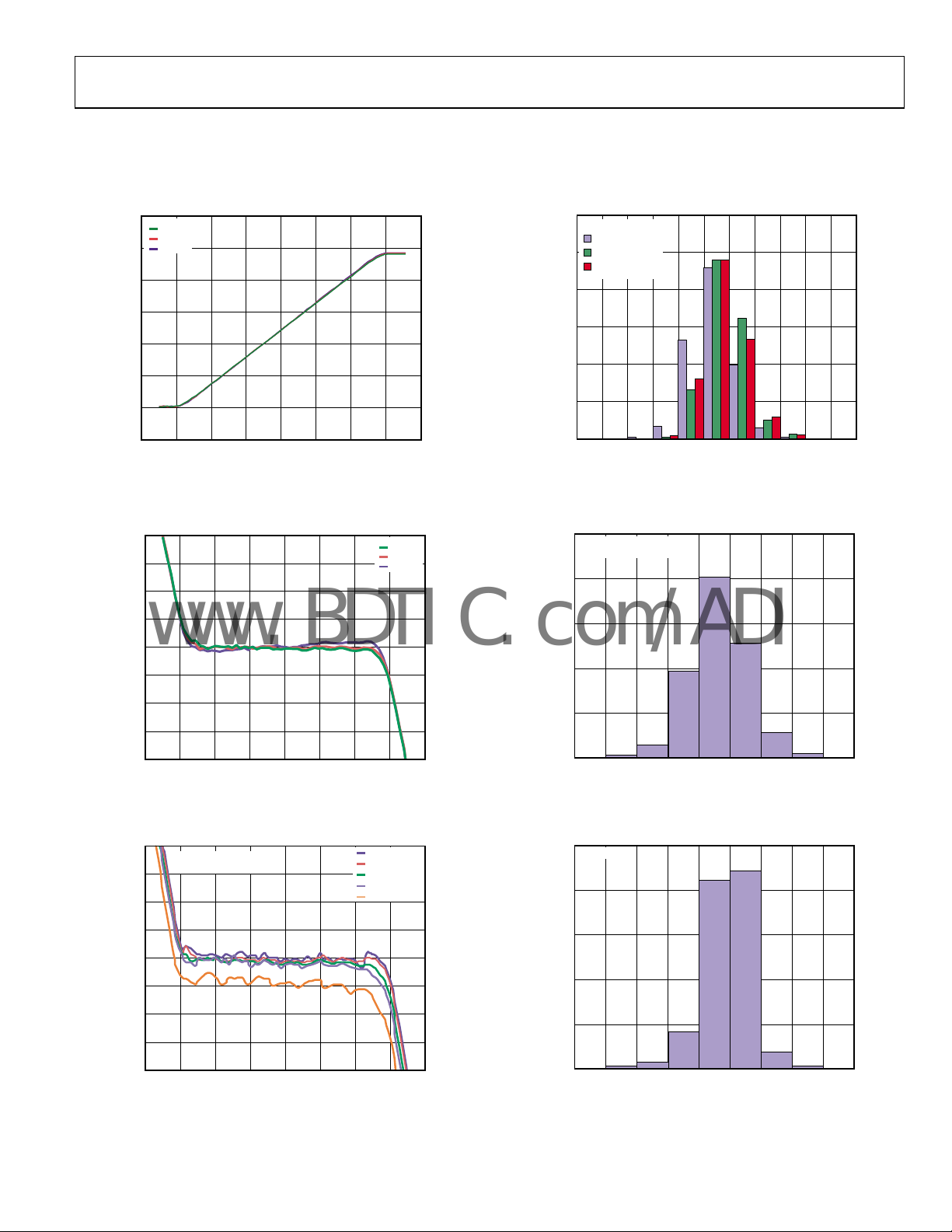
TYPICAL PERFORMANCE CHARACTERISTICS
VS = ±2.5 V, TA = 25°C, RL = 500 Ω, including a 20 Ω snubbing resistor, f = 10 MHz, CL = 2 pF, VIN = 10 mV p-p, noninverting
configuration, unless otherwise noted.
% OF UNITS
60
50
40
30
20
10
500 UNITS
V
GAIN
V
GAIN
V
GAIN
= –0.4V
=0V
= +0.4V
30
+85°C
+25°C
25
–40°C
20
15
10
GAIN (dB)
5
0
–5
–600 –200–400 400 600200 800
–800
Figure 3. Gain vs. V
2.0
1.5
1.0
0.5
0
–0.5
GAIN ERROR (dB)
–1.0
–1.5
–2.0
–600 –200–400 400 600200 800
–800
Figure 4. Gain Error vs. V
2.0
RELATIVE TO BEST FIT
LINE FOR 10MHz
1.5
1.0
0
(mV)
V
GAIN
at Three Temperatures
GAIN
(See Figure 44)
0
(mV)
V
GAIN
at Three Temperatures
GAIN
(See Figure 44)
+85°C
+25°C
–40°C
f = 1MHz
f = 10MHz
f = 70MHz
f = 100MHz
f = 150MHz
05575-003
0
–0.2
–0.3
–0.4
–0.5
0
–0.1
GAIN ERROR (dB)
0.1
0.3
0.2
Figure 6. Gain Error Histogram for Three Values of V
50
500 UNITS
–0.4V ≤ V
40
30
20
% OF UNITS
10
05575-004
0
GAIN
≤ +0.4V
19.7 20.120.019.919.819.619.3 19.4 19.5
GAIN SCALING (dB/V)
0.4
GAIN
05575-006
0.5
05575-007
Figure 7. Gain Scaling Histogram
50
500 UNITS
40
0.5
0
–0.5
GAIN ERROR (dB)
–1.0
–1.5
–2.0
–600 –200–400 400 600200 800
Figure 5. Gain Error vs. V
0–800
V
(mV)
GAIN
at Five Frequencies
GAIN
05575-005
30
20
% OF UNITS
10
0
Figure 8. Intercept Histogram
(See Figure 44)
Rev. C | Page 7 of 32
12.6
INTERCEPT (d B)
05575-008
13.012.912.812.712.512.2 12.3 12.4
AD8337
www.BDTIC.com/ADI
30
eIN = 10mV p-p
25
20
15
10
GAIN (dB)
5
0
–5
100k 500M
= +0.7
V
GAIN
V
= +0.5
GAIN
= +0.2
V
GAIN
= 0
V
GAIN
= –0.2
V
GAIN
V
= –0.5
GAIN
V
= –0.7
GAIN
1M 10M 100M
FREQUENCY (Hz)
Figure 9. Frequency Response for Various Values of V
(See Figure 45)
GAIN
05575-009
30
V
= 0V
GAIN
25
20
15
10
GAIN (dB)
5
CL = 47pF
= 22pF
C
L
0
= 10pF
C
L
= 0pF
C
L
–5
100k 500M
1M 10M 100M
FREQUENCY (Hz)
Figure 12. Frequency Response for Three Values of CL
with a 20 Ω Snubbing Resistor (See Figure 45)
05575-012
20
15
10
5
0
GAIN (dB)
–5
–10
eIN = 10mV p-p
–15
100k 500M
V
= +0.7
GAIN
V
= +0.5
GAIN
= +0.2
V
GAIN
= 0
V
GAIN
= –0.2
V
GAIN
V
= –0.5
GAIN
V
= –0.7
GAIN
1M 10M 100M
FREQUENCY (Hz)
Figure 10. Frequency Response for Various Values of V
(See Figure 58)
30
V
= 0V
GAIN
= 10mV p-p
e
IN
25
20
15
10
GAIN (dB)
5
CL = 47pF
C
= 22pF
L
0
C
= 10pF
L
C
= 0pF
L
–5
100k 500M
1M 10M 100M
FREQUENCY (Hz)
Figure 11. Frequency Response for Three Values of CL
(See Figure 45)
—Inverting Input
GAIN
10
VS = ±2.5V
= ±5V
V
S
8
6
GAIN (dB)
4
2
05575-010
0
100k 500M
1M 10M 100M
FREQUENCY (Hz)
05575-013
Figure 13. Frequency Response—Preamp
(See Figure 46)
25
20
15
10
5
GROUP DELAY (ns)
0
–5
05575-011
–10
1M 100M
10M
FREQUENCY (Hz)
05575-014
Figure 14. Group Delay vs. Frequency
(See Figure 47)
Rev. C | Page 8 of 32
AD8337
www.BDTIC.com/ADI
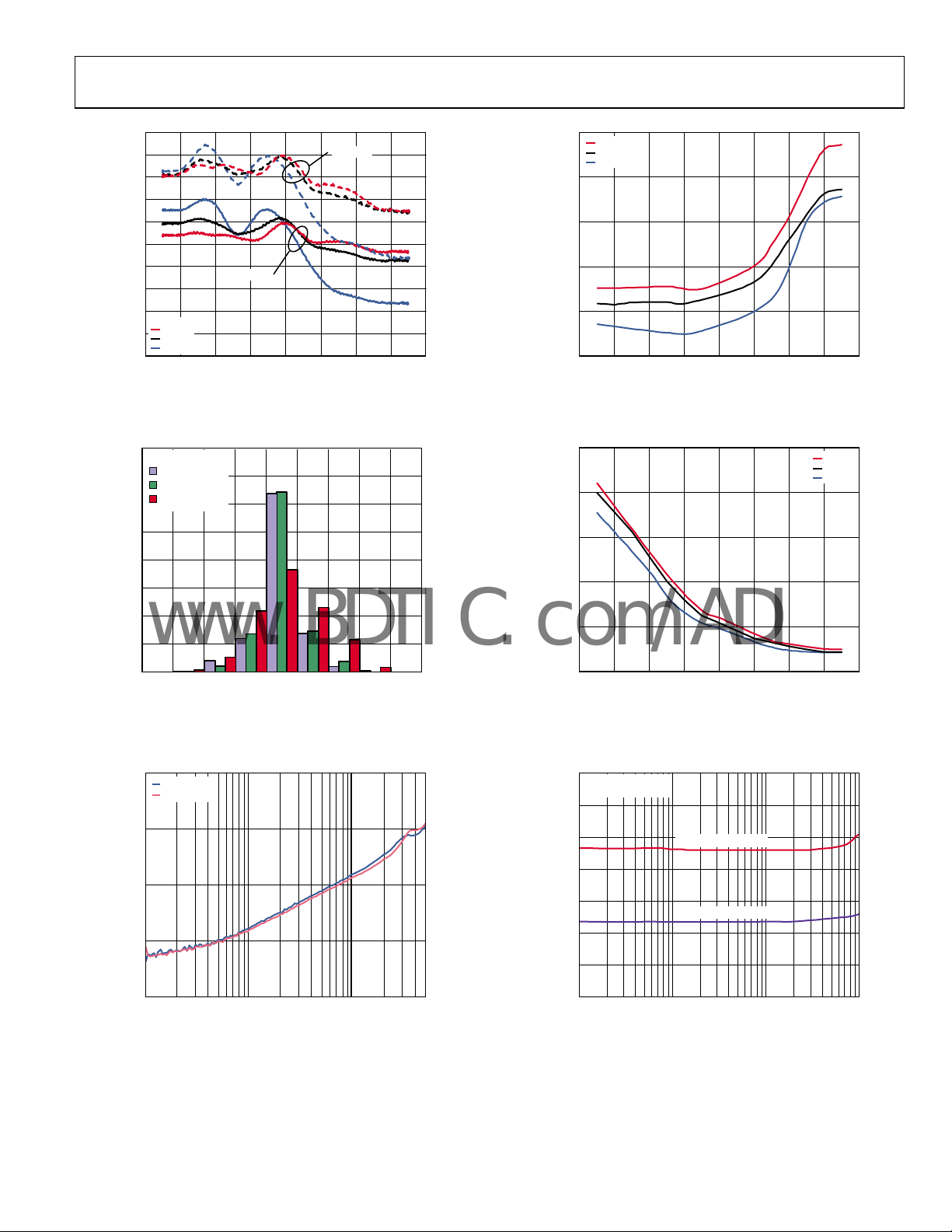
10
8
6
4
2
0
–2
–4
OFFSET VOLTAGE (mV)
–6
+85°C
–8
+25°C
–40°C
–10
–800 800
–600 –400 –200 0 200 400 600
Figure 15. Offset Voltage vs. V
VS = ±2.5V
V
GAIN
GAIN
VS = ±5V
(mV)
at Three Temperatures
(See Figure 48)
05575-015
40
+85°C
+25°C
–40°C
35
30
25
NOISE (nV/√Hz)
20
15
–800 800
–600 –200–400 400 600200
Figure 18. Output-Referred Noise vs. V
V
GAIN
0
(mV)
at Three Temperatures
GAIN
(See Figure 50)
05575-018
80
500 UNITS
V
= –0.4V
GAIN
70
60
50
40
% OF UNITS
30
20
10
0
=0V
V
GAIN
= +0.4V
V
GAIN
–15 –10 –5 0 5 10 15 20 25
OUTPUT OFFSET VOLTAGE (mV)
Figure 16. Output Offset Voltage Histogram for Three Values of V
1k
VS = ±2.5V
V
= ±5V
S
100
10
IMPEDANCE (Ω)
1
GAIN
25
20
15
10
NOISE (nV/√Hz)
5
05575-016
0
–800 800
–600 –200–400 400 600200
V
GAIN
0
(mV)
Figure 19. Short-Circuit, Input-Referred Noise at Three Temperatures
+85°C
+25°C
–40°C
05575-019
(See Figure 50)
7
V
= 0.7V
GAIN
R
= R
FB2
= 100Ω
PREAMP GAIN = –1
PREAMP GAIN = +2
FB1
6
5
4
3
NOISE (nV /√Hz)
2
1
0.1
1M 500M
FREQUENCY (Hz)
100M10M
Figure 17. VGA Output Impedance vs. Frequency
(See Figure 49)
05575-017
0
100k 100M
Figure 20. Short-Circuit, Input-Referred Noise vs. Frequency at Maximum
Gain—Inverting and Noninverting Preamp Gain = −1 and +2
Rev. C | Page 9 of 32
1M 10M
FREQUENCY (Hz)
(See Figure 50)
05575-020
AD8337
www.BDTIC.com/ADI
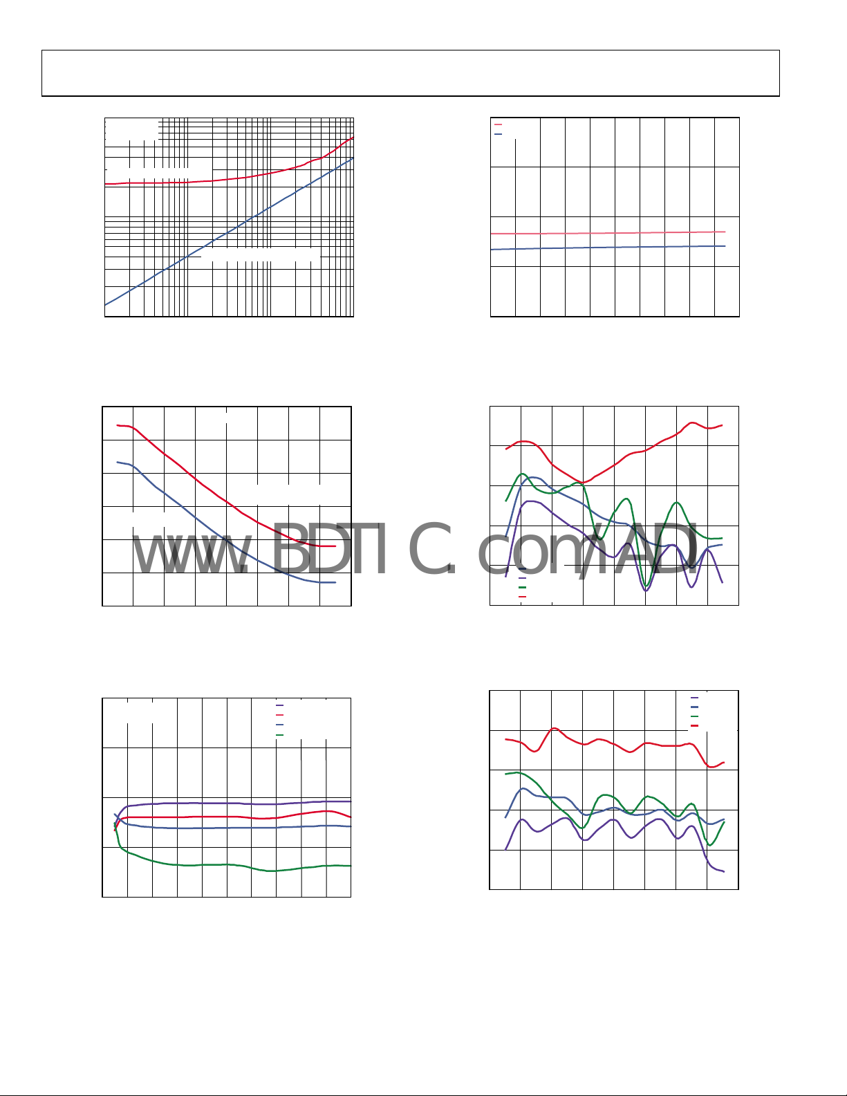
10
f = 10MHz,
V
= 0.7V
GAIN
–40
HD3
HD2
INPUT-REFE RRED NOISE
1
RS THERMAL NOISE ALONE
INPUT-REFE RRED NOISE (n V/√Hz)
0.1
11
Figure 21. Input-Referred Noise vs. R
10 100 k
SOURCE RESISTANCE (Ω)
S
05575-021
–50
–60
–70
HARMONIC DIST ORTION (dBc)
–80
05 4010 3515 3020
Figure 24. Harmonic Distortion vs. Load Capacitance
(See Figure 61)
35
30
25
20
15
NOISE FI GURE (dB)
10
5
–800
50Ω SOURCE
WITH 50Ω SHUNT
TERMINATI ON AT INPUT
UNTERMI NATED
–600 –200–400 400 600200 800
Figure 22. Noise Figure vs. V
V
GAIN
0
(mV)
GAIN
05575-022
SECOND-ORDER HARMO NIC DISTORT ION (dBc)
–30
–40
–50
–60
–70
–80
–800
–600 800–400 600–200 4000
Figure 25. HD2 vs. V
1MHz
10MHz
35MHz
100MHz
(See Figure 51)
25
LOAD CAPACITANCE (pF)
(See Figure 52)
V
GAIN
200
(mV)
GAIN
at Four Frequencies
(See Figure 52)
45 50
05575-024
05575-025
THIRD-ORDER HARMO NICDISTO RTION (dBc)
–30
–40
–50
–60
–70
–80
–800
–600 800–400 600–200 4000
Figure 26. HD3 vs. V
(See Figure 52)
–40
V
OUT
V
GAIN
–50
dBc)
–60
–70
HARMONIC DISTORTION (
–80
200 400 600 800
0
= 1V p-p
= 0V
LOAD RESIST ANCE (
HD3 VS = ±2.5V
HD3 V
HD2 V
HD2 V
Ω
)
Figure 23. Harmonic Distortion vs. RL and Supply Voltage
(See Figure 52)
= ±5V
S
= ±2.5V
S
= ±5V
S
05575-023
2.0k1.0k 1.2k 1.4k 1.6k 1.8k
Rev. C | Page 10 of 32
V
200
(mV)
GAIN
at Four Frequencies
GAIN
1MHz
10MHz
35MHz
100MHz
05575-026

AD8337
www.BDTIC.com/ADI
–30
V
= 2V p-p
OUT
= 1V p-p
V
OUT
= 0.5V p-p
V
OUT
–40
–50
–60
–70
–80
SECOND-ORDER HARMONIC DISTORT ION (dBc)
–90
–600 800–400 600–200 4000
–800
Figure 27. HD2 vs. V
–30
V
= 2V p-p
OUT
V
= 1V p-p
OUT
= 0.5V p-p
V
OUT
–40
LIMIT ED BY
MAXIMUM PREAMP
OUTPUT SWING
200
(mV)
V
GAIN
for Three Levels of Output Voltage
GAIN
(See Figure 52)
LIMITED BY
MAXIMUM PREAMP
OUTPUT SWING
05575-027
50
40
30
20
OUTPUT-REFERRED IP3 (d Bm)
10
V
= 1V p-p
OUT
TONES SEPARAT ED BY 100kHz
0
–800 –600 800–400 600–200 4000
V
GAIN
Figure 30. Output-Referred IP3 (OIP3) vs. V
at Five Frequencies (See Figure 64)
50
40
(mV)
200
GAIN
1MHz
10MHz
45MHz
70MHz
100MHz
05575-030
–50
–60
–70
–80
THIRD-ORDER HARMO NIC DISTO RTION (d Bc)
–90
–600 800–400 600–200 4000
–800
Figure 28. HD3 vs. V
–20
V
= 1V p-p
OUT
V
= 0V
GAIN
TONES SEPARATED BY 100kHz
–30
–40
–50
IMD3 (dBc)
–60
–70
–80
1M
Figure 29. IMD3 vs. Frequency
200
(mV)
V
GAIN
for Three Levels of Output Voltage
GAIN
(See Figure 52)
10M
FREQUENCY (Hz)
(See Figure 64)
VS = ±2.5V
= ±5V
V
S
100M
30
20
OUTPUT-REFERRED IP3 (dBm)
10
= ±5V
V
S
V
= 1V p-p
OUT
05575-028
TONES SEP ARATED BY 100kHz
0
–800 –600 800–400 600–200 4000
V
GAIN
200
(mV)
Figure 31. Output-Referred IP3 (OIP3) vs. V
, VS = ±5 V
GAIN
1MHz
10MHz
45MHz
70MHz
100MHz
05575-031
at Five Frequencies (See Figure 64)
20
V
= ±2.5V
S
= ±5V
V
S
15
10
5
0
–5
INPUT-REFERRED P1dB (dBm)
–10
05575-029
–15
–800 –600 800–400 600–200 4000
Figure 32. Input-Referred P1dB (IP1dB) vs. V
PREAMP LIMITED
GAIN
200
(mV)
V
GAIN
05575-032
(See Figure 63)
Rev. C | Page 11 of 32

AD8337
www.BDTIC.com/ADI
80
V
= 0.7V
GAIN
60
40
8
6
4
800
600
400
CL = 0pF
= 10pF
C
L
= 22pF
C
L
= 47pF
C
L
80
60
40
20
(mV)
0
OUT
V
–20
INPUT
–40
OUTPUT
–60
–80
–20
0
–10 302010 50 6040
TIME (ns)
Figure 33. Small Signal Pulse Response
(See Figure 53)
80
V
= 0.7V
GAIN
60
INPUT
40
20
(mV)
0
OUT
V
–20
–40
OUTPUT
–60
–80
0–20 –10 302010 50 6040
TIME (ns)
Figure 34. Small Signal Pulse Response—Inverting Feedback
(See Figure 59)
2
0
(mV)
IN
V
–2
–4
–6
–8
70
05575-033
(mV)
OUT
V
200
–200
–400
–600
–800
0
INPUT
OUTPUT
VS = ±2.5V
= 0.7V
V
GAIN
–20
0
–10 302010 50 6040 70
TIME (ns)
20
0
–20
–40
–60
–80
(mV)
IN
V
05575-036
Figure 36. Large Signal Pulse Response for Three Capacitive Loads
(See Figure 53)
(mV)
OUT
V
800
600
400
200
–200
–400
–600
–800
CL = 0pF
= 10pF
C
L
= 22pF
C
L
= 47pF
C
L
0
INPUT
OUTPUT
VS = ±5V
= 0.7V
V
GAIN
–20
0
–10 302010 50 6040
TIME (ns)
8
6
4
2
0
(mV)
IN
V
–2
–4
–6
–8
70
05575-034
80
60
40
20
0
(mV)
IN
V
–20
–40
–60
–80
70
05575-037
Figure 37. Large Signal Pulse Response for Three Capacitive Loads, VS = ±5 V
(See Figure 53)
(mV)
OUT
V
800
600
400
200
–200
–400
–600
–800
V
= 0.7V
GAIN
0
INPUT
OUTPUT
–20
0
–10 302010 50 6040 70
TIME (ns)
Figure 35. Large Signal Pulse Response
(See Figure 53)
80
60
40
20
0
(mV)
IN
V
–20
–40
–60
–80
05575-035
Rev. C | Page 12 of 32
0.8
0.6
0.4
0.2
0
(V)
–0.2
–0.4
–0.6
V
GAIN
–0.8
–0.5 0 0.5 1.0 1.5 2.0
V
OUT
TIME (µs)
Figure 38. Gain Response
(See Figure 54)
05575-038

AD8337
www.BDTIC.com/ADI
1.5
V
= 0.7V
GAIN
1.0
0.5
0
(V)
–0.5
–1.0
–1.5
–0.3 –0.1 0.1 0.3 0.5 0.7 0.9 1.1 1.3 1.5 1.7
TIME (µs)
Figure 39. Preamp Overdrive Recovery
(See Figure 55)
(V)
V
IN
V
(V)
OUT
05575-039
10
V
= +0.7V, VS= ±2.5V
GAIN
= +0.7V, VS= ±5V
V
GAIN
PSRR (dB)
–10
–20
–30
–40
–50
–60
–70
–80
0
100k
= 0V, VS= ±2.5V
V
GAIN
V
= 0V, VS= ±5V
GAIN
= –0.7V, VS= ±2.5V
V
GAIN
= –0.7V, VS= ±5V
V
GAIN
1M 100M10M
FREQUENCY (Hz)
Figure 42. PSRR vs. Frequency of Negative Supply
(See Figure 60)
05575-042
1.5
V
= 0.7V
GAIN
1.0
0.5
0
(V)
–0.5
–1.0
–1.5
–0.3 –0.1 0.1 0.3 0.5 0.7 0.9 1.1 1.3 1.5 1.7
TIME (µs)
Figure 40. VGA Overdrive Recovery
(See Figure 56)
10
V
= +0.7V, VS= ±2.5V
GAIN
= +0.7V, VS= ±5V
V
GAIN
0
V
= 0V, VS= ±2.5V
GAIN
= 0V, VS= ±5V
V
100k
GAIN
= –0.7V, VS= ±2.5V
V
GAIN
= –0.7V, VS= ±5V
V
GAIN
1M 100M10M
FREQUENCY (Hz)
–10
–20
–30
–40
PSRR (dB)
–50
–60
–70
–80
Figure 41. PSRR vs. Frequency of Positive Supply
(See Figure 60)
(V)
V
IN
V
(V)
OUT
05575-040
24
VS = ±5V
= ±2.5V
V
S
22
18
16
14
QUIESCENT S UPPLY CURRENT (mA)
12
–50
–10
–30 3010 50 702090
TEMPERATURE (° C)
05575-043
Figure 43. Quiescent Supply Current vs. Temperature
(See Figure 57)
05575-041
Rev. C | Page 13 of 32

AD8337
www.BDTIC.com/ADI
TEST CIRCUITS
NETWORK ANALYZER
NETWORK ANALYZER
49.9Ω
INOUT
50Ω
50Ω
AD8337
3
+
PrA
–
4
5 7
100Ω
100Ω
V
GAIN
Figure 44. Gain and Gain Error vs. V
NETWORK ANALYZER
OUT
50Ω 50Ω
AD8337
3
+
PrA49.9 Ω
–
4
100Ω
100Ω
57
V
IN
GAIN
20Ω 453Ω
1
GAIN
453Ω
20Ω
1
OPTIONAL
POSITIONS FOR
C
OUT
50Ω 50Ω
IN
AD8337
+
3
56.2Ω
05575-044
49.9Ω
FUNCTION
GENERATOR
PrA
–
4
5
100Ω
100Ω
7
Figure 47. Group Delay
OSCILLOSCOPE
OUT CH1 CH2
50Ω
50Ω
7
V
GAIN
50Ω
AD8337
3
+
PrA
–
4
5
L
05575-045
100Ω
100Ω
1
453Ω
20Ω
1
56.2Ω
DIFFERENTIAL
FET PROBE
453Ω
50Ω
5575-047
5575-048
49.9Ω
Figure 45. Frequency Response
NETWORK ANALYZER
OUT
50Ω 50Ω
AD8337
3
+
PrA
–
4
5
100Ω
100Ω
7
NC
IN
NC
49.9Ω
1
20Ω 453Ω
453Ω
NC
05575-046
Figure 48. Offset Voltage
NETWORK ANALYZER
AD8337
3
+
PrA
4
–
100Ω
100Ω
Figure 46. Frequency Response—Preamp
Figure 49. Output Impedance vs. Frequency
Rev. C | Page 14 of 32
CONFIGURE T O
MEASURE Z
CONVERT ED S11
IN
50Ω
0Ω
0Ω
1
7
5
NC
05575-049

AD8337
www.BDTIC.com/ADI
SPECTRUM ANALYZ E
50Ω
R
IN
PULSE
GENERATOR
OUT
POWER
SPLITTER
OSCILLOSCOPE
CH1
50Ω
CH2
50Ω
AD8337
3
49.9Ω
4
100Ω
+
PrA
–
100Ω
5
7
V
GAIN
0Ω
1
Figure 50. Input-Referred and Output-Referred Noise
NOISE FI GURE METER
NOISE
SOURCE
NOISE
SOURCE
DRIVE
INPUT
0Ω
AD8337
3
49.9Ω
(OR ∞)
+
PrA
4
–
5
100Ω
100Ω
Figure 51. Noise Figure vs. V
7
V
GAIN
GAIN
0Ω
1
0Ω
3
4
49.9Ω
100Ω
05575-050
+
PrA
–
100Ω
AD8337
5
20Ω 453Ω
1
56.2Ω
7
0.7V
05575-053
Figure 53. Pulse Response
DUAL
FUNCTION
GENERATOR
POWER
SPLITTER
SINE
WAVE
SQUARE
WAVE
AD8337
3
+
49.9Ω
05575-051
4
100Ω
PrA
–
100Ω
OSCILLOSCOPE
CH1
5
50Ω
7
V
50Ω
GAIN
1
CH2
DIFFERENTIAL
FET PROBE
20Ω 453Ω
NC
05575-054
Figure 54. Gain Response
SIGNAL
GENERATOR
LOWPASS
FILTER
SPECTRUM ANALYZ ER
INPUT
50Ω
R
L
FUNCTION
GENERATOR
OUTPUT
AD8337
3
+
4
100Ω
PrA
–
100Ω
49.9Ω
Figure 52. Harmonic Distortion
5
7
V
GAIN
20Ω
1
C
L
49.9Ω
05575-052
3
4
100Ω
Figure 55. Preamp Overdrive Recovery
Rev. C | Page 15 of 32
AD8337
+
PrA
–
100Ω
OSCILLOSCOPE
CH1
NC
5
7
100Ω
50Ω
1
CH2
NC
05575-055

AD8337
www.BDTIC.com/ADI
FUNCTION
GENERATOR
OUTPUT
49.9Ω
POWER
SPLITTER
AD8337
3
+
PrA
–
4
100Ω
100Ω
Figure 56. VGA Overdrive Recovery
AD8337
3
+
PrA
4
–
100Ω
100Ω
Figure 57. Supply Current
CH1
5
5
OSCILLOSCOPE
50Ω50Ω
1
DMM
(+I)
8
1
7
6
DMM
(–I)
CH2
20Ω 453 Ω
DMM
(V)
PULSE
GENERATOR
OUT
POWER
SPLITTER
OSCILLO SCOPE
CH1
50Ω
CH2
50Ω
AD8337
NC
3
+
PrA 1
4
100Ω
100Ω
05575-056
–
100Ω
5
7
0.7V
20Ω 453Ω
56.2Ω
05575-059
Figure 59. Pulse Response—Inverting Feedback
+SUPPLY TO NETWORK
ANALYZER BIAS PORT
BENCH
POWER SUPPLY
BYPASS
CAPACITORS
REMOVE D FOR
MEASUREMENT
3
49.9Ω
4
100Ω
05575-057
NETWORK ANALYZER
VPOS
+
PrA
–
5
100Ω
50Ω
AD8337
7
V
50Ω
GAIN
INOUT
1
DIFFERENTIAL
FET PROBE
05575-060
Figure 60. PSRR
NETWORK ANALYZER
INOUT
50Ω
50Ω
AD8337
+
3
100Ω
100Ω
PrA
–
4
5
100Ω
7
V
GAIN
Figure 58. Frequency Response—Inverting Feedback
453Ω
20Ω
1
05575-058
Figure 61. Input-Referred Noise vs. RS
SPECTRUM ANALYZ ER
3
+
4
–
100Ω
100Ω
Rev. C | Page 16 of 32
PrA
50Ω
AD8337
5
IN
1
7
V
GAIN
05575-061

AD8337
www.BDTIC.com/ADI
NETWORK ANALY ZER
SPECTRUM ANALYZ ER
POWER SWEEP
IN
50Ω
AD8337
3
+
PrA 1
–
4
5
100Ω
100Ω
7
0.7V
05575-062
Figure 62. Short-Circuit Input Noise vs. Frequency
22dB
49.9Ω
+
3
PrA
–
4
100Ω
100Ω
Figure 63. IP1dB vs. V
50Ω
AD8337
5
50Ω
INOUT
453Ω
20Ω
1
7
V
GAIN
05575-063
GAIN
SPECTRUM ANALYZ ER
INPUT
50Ω
SIGNAL
GENERATOR
SIGNAL
GENERATOR
+22dB –6dB
+22dB –6dB
COMBINER
–6dB
49.9Ω
3
4
100Ω
+
PrA
–
100Ω
AD8337
5
7
V
GAIN
1
–6dB
20Ω
453Ω
05575-064
Figure 64. IMD and OIP3
Rev. C | Page 17 of 32

AD8337
www.BDTIC.com/ADI
THEORY OF OPERATION
VPOS
R
= R
+
PrA
6dB
–
BIAS
FB2
= 100Ω
FB1
INPP
3
R
INPN
PRAO
R
FB2
FB1
4
5
R
G
8
+
ATTENUATOR
–24dB TO 0d B
–
INTERP OLAT OR
+
18dB
(8x)
–
GAIN
INTERFACE
749Ω
107Ω
1
VOUT
VCOM
Figure 65. Circuit Block Diagram
OVERVIEW
The AD8337 is a low noise, single-ended, linear-in-dB, generalpurpose variable gain amplifier (VGA) usable at frequencies up
to 100 MHz. It is fabricated using a proprietary Analog Devices
dielectrically isolated, complementary bipolar process. The
bandwidth is dc to 280 MHz and features low dc offset voltage
and an ideal nominal gain range of 0 dB to 24 dB. Requiring
about 15.5 mA, the power consumption is only 78 mW from
either a single +5 V or a dual ±2.5 V supply. Figure 65 is the
circuit block diagram of the AD8337.
PREAMPLIFIER
An uncommitted current-feedback op amp included in the
AD8337 can be used as a preamplifier to buffer the ladder
network attenuator of the X-AMP. As with any op amp, the gain
is established using external resistors, and the preamplifier is
specified with a noninverting gain of 6 dB (2×) and gain resistor
values of 100 Ω. The preamplifier gain can be increased using
larger values of R
The value of R
internal compensation capacitor determine the 3 dB bandwidth,
and smaller values can compromise preamplifier stability.
Because the AD8337 is dc-coupled, larger preamp gains increase
the offset voltage. The offset voltage can be compensated by
connecting a resistor between the INPN input and the supply
voltage. If the offset is negative, the resistor value connects to
the negative supply. For ease of adjustment, a trimmer network
can be used.
For larger gains, the overall noise is reduced if a low value of
R
is selected. For values of R
FB1
preamp gain is 16× (24.1 dB), and the input-referred noise is
approximately 1.5 nV/√Hz. For this value of gain, the overall
gain range increases by 18 dB; therefore, the gain range is 18 dB
to 42 dB.
, trading off bandwidth and offset voltage.
FB2
is to be ≥100 Ω because the value and an
FB2
= 20 Ω and R
FB1
= 301 Ω, the
FB2
2
6
VNEG
7
GAIN
05575-065
VGA
This X-AMP, with its linear-in-dB gain characteristic
architecture, yields the optimum dynamic range for receiver
applications. Referring to Figure 65, the signal path consists of
a −24 dB variable attenuator followed by a fixed gain amplifier of
18 dB, for a total VGA gain range of −6 dB to +18 dB. With the
preamplifier configured for a gain of 6 dB, the composite gain
range is 0 dB to 24 dB.
The VGA plus preamp, with 6 dB of gain, implements the
following exact gain law:
dB
⎡
19.7(dB) ICPT
⎢
⎣
×=
VGain +
V
GAIN
⎤
⎥
⎦
(dB)
where the nominal intercept (ICPT) = 12.65 dB.
The ICPT increases as the gain of the preamp is increased. For
example, if the gain of the preamp is increased by 6 dB, ICPT
increases to 18.65 dB. Although the previous equation shows
the exact gain law as based on statistical data, a quick estimation
of signal levels can be made using the default slope of 20 dB/V
for a particular gain setting. For example, the change in gain for
a V
change of 0.3 V is 6 dB using a slope of 20 dB/V and
GAIN
5.91 dB using the exact slope of 19.6 dB/V. This is a difference
of only 0.09 dB.
GAIN CONTROL
The gain control interface provides a high impedance input and
is referenced to the VCOM pin (in a single-supply application to
midsupply at [VPOS + VNEG]/2 for optimum swing). When
dual supplies are used, VCOM is connected to ground. The voltage
on the VCOM pin determines the midpoint of the gain range. For
a ground referenced design, the VGAIN range is from −0.7 V to
+0.7 V with the most linear-in-dB section of the gain control
between −0.6 V and +0.6 V. In the center 80% of the VGAIN
range, the gain error is typically less than ±0.2 dB. The gain
control voltage can be increased or decreased to the positive or
negative rails without gain foldover.
Rev. C | Page 18 of 32

AD8337
www.BDTIC.com/ADI
The gain scaling factor (gain slope) is designed for 20 dB/V. This
relatively low slope ensures that noise on the GAIN input is not
unduly amplified. Because a VGA functions as a multiplier, it is
important that the GAIN input does not inadvertently modulate
the output signal with unwanted noise. Because of its high input
impedance, a simple low-pass filter can be added to the GAIN
input to filter unwanted noise.
OUTPUT STAGE
The output stage is a Class AB, voltage-feedback, complementary
emitter-follower with a fixed gain of 18 dB, similar to the preamplifier in speed and bandwidth. Because of the ac-beta roll-off
of the output devices and the inherent reduction in feedback
beyond the −3 dB bandwidth, the impedance looking into the
output pin of the preamp and output stages appears to be inductive
(increasing impedance with increasing frequency). The high
speed output amplifier used in the AD8337 can drive large
currents, but its stability is susceptible to capacitive loading.
A small series resistor mitigates the effects of capacitive loading
(see the Applications Information section).
ATTENUATOR
The input resistance of the VGA attenuator is nominally 265 Ω.
For example, if the default preamplifier feedback network R
R
is 200 Ω, the effective preamplifier load is approximately
FB2
FB1
+
114 Ω. The attenuator is composed of eight 3.01 dB sections for
a total attenuation range of −24.08 dB. Following the attenuator
is a fixed gain amplifier with 8× (18.06 dB) gain. Because of this
relatively low gain, the output offset is kept well below 20 mV
over temperature; the offset is largest at maximum gain when
the preamplifier offset is amplified. The VCOM pin defines the
common-mode reference for the output, as shown in Figure 65.
SINGLE-SUPPLY OPERATION AND AC COUPLING
If the AD8337 is to be operated from a single 5 V supply, the
bias supply for VCOM must be a very low impedance 2.5 V
reference, especially if dc coupling is used. If the device is dccoupled, the VCOM source must be able to handle the preamplifier
and VGA dynamic load currents in addition to the bias currents.
When ac coupling the preamplifier input, a bias network and
bypass capacitor must be connected to the opposite polarity
input pin. The bias generator for the VCOM pin must provide
the dynamic current to the preamplifier feedback network and
the VGA attenuator. For many single 5 V applications, a reference, such as the ADR391, and a good op amp provide an
adequate VCOM source if a 2.5 V supply is unavailable.
NOISE
The total input-referred voltage and current noise of the positive
input of the preamplifier are about 2.2 nV/√Hz and 4.8 pA/√Hz.
The VGA output-referred noise is about 21 nV/√Hz at low gains.
This result is divided by the VGA fixed gain amplifier gain of 8×
and results in a voltage noise density of 2.6 nV/√Hz referred to
the VGA input. This value includes the noise of the VGA gain
setting resistors as well. If this voltage is again divided by the
preamp gain of 2, the VGA noise referred all the way to the
preamp input is about 1.3 nV/√Hz. From this, it is determined
that the preamplifier, including the 100 Ω gain setting resistors,
contributes about 1.8 nV/√Hz. The two 100 Ω resistors contribute
1.29 nV/√Hz each at the output of the preamp. With the gain
resistor noise subtracted, the preamplifier noise is approximately
1.55 nV/√Hz.
Equation 2 shows the calculation that determines the output-
referred noise at maximum gain (24 dB or 16×).
where:
A
is the total gain from preamp input to VGA output.
t
is the source resistance.
R
S
e
is the input-referred voltage noise of the preamp.
n − PrA
is the current noise of the preamp at the INPP pin.
i
n − PrA
e
is the voltage noise of R
n −
R
1FB
is the voltage noise of R
e
n −
R
2FB
e
is the input-referred voltage noise of the VGA (low gain,
n − VGA
output-referred noise divided by a fixed gain of 8×).
Assuming R
= 0 Ω, R
S
FB1
= R
8×, the noise simplifies to
e
= HznV 35 8) (1.9 8) 2(1.29 16) (1.75
n − out
Dividing the result by 16 gives the total input-referred noise with
a short-circuited input as 2.2 nV/√Hz. When the preamplifier is
used in the inverting configuration with the same R
100 Ω as previously noted, e
because the gain dropped by 6 dB, the input-referred noise
increases by a factor of 2 to about 4.4 nV/√Hz. The reason for this
increase is that the noise gain to the output of the noise generators
stays the same, yet the preamp in the inverting configuration has a
gain of −1 compared to the +2 in the noninverting configuration;
this increases the input-referred noise by 2.
.
FB1
.
FB2
= 100 Ω, At = 16×, and A
FB2
222
=×+×+× (1)
FB1
does not change. However,
n − out
and R
VGA
FB2
=
=
e
−
n
Rne
t
S
−
n
2
+×=
)(
(e
A
2
+×
(i
)tA
−
n
2
+×
(e
)SR
n
R
R
FB2
FB1
−
A
VGA
2
+××
(e
)
−
n
FB2FB1
Rev. C | Page 19 of 32
A
VGA
2
+×
(e
)
×
−
n
VGARRPrAPrAout
A
VGA
2
)
(2)

AD8337
www.BDTIC.com/ADI
APPLICATIONS INFORMATION
PREAMPLIFIER CONNECTIONS
Noninverting Gain Configuration
The AD8337 preamplifier is an uncommitted current-feedback
op amp that is stable for values of R
for the noninverting feedback connections.
INPP
3
R
G
R
PRAO
R
FB2
FB1
INPN
4
5
Figure 66. AD8337 Preamplifier Configured for Noninverting Gain
Two surface-mount resistors establish the preamplifier gain.
Equal values of 100 Ω configure the preamplifier for a 6 dB gain
and the device for a default gain range of 0 dB to 24 dB.
For preamplifier gains ≥2, select a value of R
≤ 100 Ω. Higher values of R
R
FB1
increase the offset voltage, but smaller values compromise
stability. If R
≤ 100 Ω, the gain increases and the input-
FB1
referred noise decreases.
Inverting Gain Configuration
For applications requiring polarity inversion of negative pulses, or
for waveforms that require current sinking, the preamplifier can
be configured as an inverting gain amplifier. When configured
with bipolar supplies, the preamplifier amplifies positive or
negative input voltages with no level shifting of the commonmode input voltage required. Figure 67 shows the AD8337
configured for inverting gain operation.
Because the AD8337 is a very high frequency device, stability
issues can occur unless the circuit board on which it is used is
carefully laid out. The stability of the preamp is affected by
parasitic capacitance around the INPN pin. To minimize stray
capacitance position the preamp gain resistors, R
close as possible to the INPN pin.
INPP
3
R
Figure 67. The AD8337 Preamplifier Configured for Inverting Gain
FB1
INPN
PRAO
R
FB2
4
5
≥ 100 Ω. See Figure 66
FB2
PREAMPLIFIER
+
–
05575-066
≥ 100 Ω and
FB2
reduce the bandwidth and
FB2
and R
FB1
PREAMPLIFIER
+
–
05575-067
FB2
, as
DRIVING CAPACITIVE LOADS
Because of the large bandwidth of the AD8337, stray capacitance at
the output pin can induce peaking in the frequency response as the
gain of the amplifier begins to roll off. Figure 68 shows peaking
with two values of load capacitance using ±2.5 V supplies and
= 0 V.
V
GAIN
25
V
= 0V
GAIN
CL = 0pF
= 10pF
C
L
C
= 22pF
20
L
NO SNUBBING RESIST OR
15
10
GAIN (dB)
5
0
–5
100k
1M 500M100M10M
FREQUENC Y (Hz)
Figure 68. Peaking in the Frequency Response for Two Values of Output
Capacitance with ±2.5 V Supplies and No Snubbing Resistor
25
V
= 0V
GAIN
CL = 0pF
= 10pF
C
L
20
C
= 22pF
L
WITH 20Ω SNUBBING RESIST OR
15
10
GAIN (dB)
5
0
–5
100k
1M 500M100M10M
FREQUENC Y (Hz)
Figure 69. Frequency Response for Two Values of Output Capacitance
with a 20 Ω Snubbing Resistor
In the time domain, stray capacitance at the output pin can
induce overshoot on the edges of transient signals, as shown in
Figure 70 and Figure 72. The amplitude of the overshoot is also a
function of the slewing of the transient (not shown in Figure 70
and Figure 72). The transition time of the input pulses used for
Figure 70 and Figure 72 is deliberately set high at 300 ps to demonstrate the fast response time of the amplifier. Signals with longer
transition times generate less overshoot.
05575-068
05575-069
Rev. C | Page 20 of 32

AD8337
www.BDTIC.com/ADI
800
600
400
200
(mV)
0
OUT
V
–200
INPUT
–400
OUTPUT
–600
–800
–20
–10 302010 50 6040 80
CL = 0pF
C
= 10pF
L
C
= 22pF
L
NO SNUBBING RESISTO R
0
TIME (ns)
70
Figure 70. Pulse Response for Two Values of Output Capacitance
with ±2.5 V Supplies and No Snubbing Resistor
800
600
400
200
(mV)
0
OUT
V
–200
INPUT
OUTPUT
–400
–600
–800
–20
–10 302010 50 6040 80
CL = 0pF
= 10pF
C
L
C
= 22pF
L
WITH 20Ω SNUBBING RESISTOR
0
TIME (ns)
Figure 71. Pulse Response for Two Values of Output Capacitance
with ±2.5 V Supplies and a 20 Ω Snubbing Resistor
800
VS = ±5V
600
400
200
(mV)
0
OUT
V
–200
INPUT
–400
OUTPUT
–600
–800
–20
–10 302010 50 6040 80
CL = 0pF
= 10pF
C
L
= 22pF
C
L
WITH NO SNUBBING RESIST OR
0
TIME (ns)
Figure 72. Large Signal Pulse Response for Two Values of Output
Capacitance with ±5 V Supplies and No Snubbing Resistor
80
60
40
20
0
–20
–40
–60
–80
(mV)
IN
V
05575-070
(mV)
V
800
600
400
200
OUT
–200
–400
–600
–800
VS = ±5V
0
INPUT
OUTPUT
–20
–10 302010 50 6040 80
CL = 0pF
= 10pF
C
L
= 22pF
C
L
WITH 20Ω SNUBBING RESISTOR
0
TIME (ns)
80
60
40
20
0
(mV)
IN
V
–20
–40
–60
–80
70
05575-073
Figure 73. Pulse Response for Two Values of Output Capacitance
80
60
40
20
0
–20
–40
–60
The effects of stray output capacitance are mitigated with a
small value snubbing resistor, R
as near as possible to, the VOUT pin. Figure 69, Figure 71, and
Figure 73 show the improvement in dynamic performance with
a 20 snubbing resistor. R
(mV)
IN
V
ratio of R
impedance loads, such as ADCs. For other loads, alternate values
of R
SNUB
the Typical Performance Characteristics section are derived using
a 20 Ω snubbing resistor.
with ±5 V Supplies and a 20 Ω Snubbing Resistor
, placed in series with, and
SNUB
reduces the gain slightly by the
SNUB
/(R
+ RL), a very small loss when used with high
L
SNUB
can be determined empirically. The data for the curves in
The best way to avoid the effects of stray capacitance is to
–80
70
05575-071
exercise care in the PCB layout. Locate the passive components
or devices connected to the AD8337 output pins as close as
possible to the package.
80
60
40
20
0
(mV)
IN
V
–20
–40
–60
–80
70
05575-072
Although a nonissue, the preamplifier output is also sensitive to
load capacitance. However, the series connection of R
R
is typically the only load connected to the preamplifier. If
FB2
FB1
and
overshoot appears, it can be mitigated by inserting a snubbing
resistor, the same way as the VGA output.
GAIN CONTROL CONSIDERATIONS
In typical applications, voltages applied to the GAIN input are dc
or relatively low frequency signals. The high input impedance of
the AD8337 enables several devices to be connected in parallel.
This is useful for arrays of VGAs, such as those used for calibration adjustments.
Under dc or slowly changing ramp conditions, the gain tracks
the gain control voltage, as shown in Figure 3. However, it is often
necessary to consider other effects influenced by the V
GAIN
input.
Rev. C | Page 21 of 32

AD8337
www.BDTIC.com/ADI
The offset voltage effect of the AD8337, as with all VGAs, can
appear as a complex waveform when observed across the range
of V
a unique offset voltage (V
voltage. Generated by multiple sources, each device has
GAIN
) profile while the GAIN input is
OS
swept through its voltage range. The offset voltage profile seen
in Figure 15 is a typical example. If the V
modulated, the output is the product of the V
input voltage is
GAIN
and the dc
GAIN
profile of the offset voltage. This is observed on a scope as a
small ac signal, as shown in Figure 74. In Figure 74, the signal
applied to the V
input is a 1 kHz ramp, and the output voltage
GAIN
signal is slightly less than 4 mV p-p.
10
VS = ±2.5V
INPUT
OFFSET VOLTAGE (mV)
–10
8
6
4
2
0
–2
–4
–6
–8
–800
2.5
VS=
OUTPUT
–600 –200–400 400 600200 800
Figure 74. Offset Voltage vs. V
V
GAIN
0
(mV)
for a 1 kHz Ramp
GAIN
05575-075
The profile of the waveform shown in Figure 74 is consistent
over a wide range of signals from dc to about 20 kHz. Above
20 kHz, secondary artifacts can be generated due to the effects
of minor internal circuit tolerances, as shown in Figure 75.
These artifacts are caused by settling and time constants of the
interpolator circuit and appear at the output as the voltage
spikes, as shown in Figure 75.
10
VS = ±2.5V
8
INPUT
2.5
VS=
OUTPUT
6
4
2
0
–2
–4
OFFSET VOLTAGE (mV)
–6
–8
–10
–800
–600 –200–400 400 600200 800
Figure 75. V
SPIKE
0
V
(mV)
GAIN
Profile for a 50 kHz Ramp
OS
SPIKE
05575-074
Under certain circumstances, the product of V
offset profile plus spikes is a coherent spurious signal within the
signal band of interest and indistinguishable from desired
signals. In general, the slower the ramp applied to the GAIN
Pin, the smaller the spikes are. In most applications, these
effects are benign and not an issue.
THERMAL CONSIDERATIONS
The thermal performance of LFCSPs, such as the AD8337,
departs significantly from that of leaded devices such as the
larger TSSOP or QFSP. In larger packages, heat is conducted
away from the die by the path provided by the bond wires and
the device leads. In LFCSPs, the heat transfer mechanisms are
surface-to-air radiation from the top and side surfaces of the
package and conduction through the metal solder pad on the
mounting surface of the device.
θ
is the traditional thermal metric used for integrated circuits.
JC
Heat transfer away from the die is a three-dimensional dynamic,
and the path is through the bond wires, leads, and the six
surfaces of the package. Because of the small size of LFCSPs, the
is not measured conventionally. Instead, it is calculated using
θ
JC
thermodynamic rules.
The θ
value of the AD8837 listed in Table 2 assumes that the
JC
tab is soldered to the board and that there are three additional
ground layers beneath the device connected by at least four vias.
For a device with an unsoldered pad, the θ
becoming 138°C/W.
PSI (Ψ)
Table 2 lists a subset of the classic theta specification, ΨJT (Psi
junction to top). θ
is the metric of heat transfer from the die to
JC
the case, involving the six outside surfaces of the package. Ψ
is a subset of the theta value and the thermal gradient from the
junction (die) to each of the six surfaces. Ψ can be different for
each of the surfaces, but since the top of the package is a fraction of
a millimeter from the die, the surface temperature of the package is
very close to the die temperature. The die temperature is calculated
as the product of the power dissipation and Ψ
surface temperature and power dissipation are easily measured, it
follows that the die temperature is easily calculated. For example,
for a dissipation of 180 mW and a Ψ
of 5.3°C/W, the die
JT
temperature is slightly less than 1°C higher than the surface
temperature.
BOARD LAYOUT
Because the AD8337 is a high frequency device, board layout is
critical. It is very important to have a good ground plane
connection to the VCOM pin. Coupling through the ground
plane, from the output to the input, can cause peaking at higher
frequencies.
and the
GAIN
nearly doubles,
JC
. Since the top
JT
(XY)
Rev. C | Page 22 of 32

AD8337
www.BDTIC.com/ADI
EVALUATION BOARDS
The AD8337evaluation boards provide a family of platforms for
testing and evaluating the AD8337 VGA. Three circuit configurations are available:
• AD8337-EVALZ, dc-coupled, with noninverting gain and
dual power supplies
• AD8337-EVALZ-INV, dc-coupled, with inverting gain and
dual power supplies
• AD8337-EVALZ-SS, ac-coupled, with noninverting gain
configuration and a single supply
These fully assembled and tested boards are ready to use. Only
the appropriate power supply and signal source connections
need to be made. SMA connectors are provided for the preamplifier (PrA) and VGA outputs. Photos of fully assembled boards
are shown in Figure 76 and Figure 77. The board component
side layouts are shown in Figure 78 and Figure 79.
Figure 78. Assembly, Dual-Supply Evaluation Board
05575-178
Figure 76. AD8337 Evaluation Board for dual Supplies
Figure 77. AD8337 Evaluation Board for Single Supply
05575-176
Schematic diagrams of the dual-supply board for noninverting
and inverting configurations are shown in Figure 80 and Figure 81.
The du
of sup
single-supply board is shown in Figure 82. The single supply
version accepts a +5 V to +10 V supply with 20 mA or greater
capability.
05575-177
Rev. C | Page 23 of 32
Figure 79. Assembly, Single-Supply Evaluation Board
al-supply boards require ±2.5 V to ±5 V supplies capable
plying 20 mA or greater. A schematic diagram of the
05575-179

AD8337
www.BDTIC.com/ADI
GND1 GND2G ND GND3 GND4
RVO1
VOUT
453Ω
TP1
J1
R4
IN
0Ω
49.9Ω
R5
100Ω
RVO3
0Ω
R2
1
VOUT
U1
AD8337
2
VCOM
3
INPP
R
FB2
100Ω
R
FB1
100Ω
DO NOT INST ALL PARTS IN GRAY
VPOS
GAIN
VNEG
PRAOINPN
8
7
6
54
10µF
C3
0.1µF
C4
0.1µF
C1
+
120nH
CG
1nF
+V
L2
RPO2
453Ω
S
R1
49.9Ω
GAIN
Figure 80. Schematic—AD8337-EVALZ - Noninverting Configuration
+V
C1
C3
0.1µF
CG
1nF
+
120nH
L2
RPO2
453Ω
S
R1
49.9Ω
GAIN
100Ω
IN
VOUT
TP1
J1
49.9Ω
R5
100Ω
GND1 GND2G ND GND3 GND4
RVO1
453Ω
1
2
3
R
FB1
100Ω
VOUT
VCOM
INPP
R4
0Ω
RVO3
0Ω
R2
10µF
8
VPOS
U1
AD8337
R
FB2
100Ω
DO NOT INST ALL PARTS IN GRAY
GAIN
VNEG
PRAOINPN
7
6
54
C4
0.1µF
Figure 81. Schematic—AD8337-EVALZ-INV Inverting Configuration
+V
S
GND1
GND2 GND3 GND4
C4
0.1µF
C10
0.1µF
12
VIN
SHDN
VOUT
U2
GND
5
ADR391AUJZ-R2
3
4
C9
0.1µF
AD8541AR
3
2
0.22µF
U3
C8
Figure 82. Evaluation Board Schematic—Single-Supply Version
–V
S
+
L1
120nH
PRAO
–V
S
L1
120nH
PRAO
+
C1
10µF
10V
IN
C7
0.1µF
7
100Ω
6
4
R4
10kΩ
Rev. C | Page 24 of 32
C2
10µF
+
C6
0.1µF
49.9Ω
R6
C2
10µF
05575-180
05575-181
L1
120nH FB
R1
1µF
16V
CIRCUIT OPTIONS
Part numbers for fully assembled boards are listed in Table 4.
Table 4. AD8337 Evaluation Board Variations
Part Number Configuration
AD8337-EVALZ Dual-supply noninverting
AD8337-EVALZ-INV Dual-supply inverting
AD8337-EVALZ-SS Single-supply noninverting
Figure 80, Figure 81, and Figure 82 are schematics for the
various circuit configurations. Within limits, the AD8337
preamplifier gain is controlled by Resistor R
. For simple guidelines applying to the current-feedback
R
FB2
and Resistor
FB1
preamplifier, see the Theory of Operation section.
OUTPUT PROTECTION
The AD8337 VGA output stage is specified for driving loads of
500 Ω or greater. To protect the stage from an accidental
overload, a 453 Ω resistor is provided, which when connected to
50 Ω test equipment inputs, enables safe operation. In certain
high load impedance situations, the value of this resistor can be
reduced. However, if load capacitance values greater than
approximately 20 pF are anticipated, such as a BNC cable, the
minimum series resistor value is not to be less than 20 Ω.
An alternate test pin is also provided for direct access to the
output of the AD8337 VGA. The pin is typically used for a
probe, and a 0 Ω resistor is provided between the test loop and
the output pin. If the test loop is connected to loads ≤500 Ω,
then the 0 Ω resistor is to be changed to an appropriate value.
C3
0.1µF
8
VPOS
3
INPN PRAO
R
FB1
100Ω
+
C2
R
FB2
100Ω
U1
AD8337
5
C5
0.1µF
VCOM
2
VOUTINPP
GAIN
VNEG
RVO1
453Ω
1
7
64
CG
1nF
VOUT
GAIN
05575-182

AD8337
www.BDTIC.com/ADI
TOP:
SIGN A L GEN ER AT OR 10.05M Hz, 500mV p- p
BOTTOM:
SIGN A L GEN ER AT OR 9.95M Hz, 500mV p- p
POWER
SIGNAL
INPUT
AMPLIFIERS
POWER
SPLITTER
SPECTRUM
ANALYZER
PREAMP
OUTPU T
Figure 83. Typical Board Test Connections
MEASUREMENT SETUP
Figure 83 shows board connections for two generators. In this
example, the experiment illustrates IMD measurements using
standard off-the-shelf test equipment used by Analog Devices.
However, any equivalent equipment can be used.
BOARD LAYOUT CONSIDERATIONS
The AD8337 evaluation board is designed using four layers.
Interconnecting circuitry is located on the component and
wiring sides, with the inner layers dedicated to power and
ground planes. Figure 84 through Figure 88 show the copper
layouts.
–5V
POWER SUPPLY
For ease of assembly, all board components are located on the
primary side and are 0603 size surface mounts. Higher density
applications may require components on both sides of the board
and present no problem to the AD8337, as demonstrated in
unreleased versions of the board that featured secondary-side
components and vias. Not evident in the figures are thermal
vias within the pad that solder to the mating pad of the AD8337
chip-scale package. These vias serve as a thermal path and are
the primary means of removing heat from the device. The thermal
specifications for the AD8337 are predicated on the use of multilayer board construction with these thermal vias to enable heat
conductivity from the die.
+5V
VGAIN
05575-183
Rev. C | Page 25 of 32

AD8337
www.BDTIC.com/ADI
5575-113
05575-109
Figure 84. Dual-Supply Component Side Copper
Figure 88. Dual-Supply Power Plane
05575-110
Figure 85. Dual-Supply Wiring Side Copper
05575-111
Figure 86. Dual-Supply Component Side Silk-Screen
Figure 89. Single-Supply Component Side Copper
05575-115
Figure 90. Single-Supply Wiring Side Copper
05575-114
05575-112
Figure 87. Dual-Supply Ground Plane
Rev. C | Page 26 of 32
Figure 91. Single-Supply Component Side Silkscreen
05575-116

AD8337
www.BDTIC.com/ADI
05575-117
Figure 92. Single-Supply Ground Plane
Figure 93. Single-Supply Power Plane
05575-118
BILL OF MATERIALS
Table 5. Dual-Supply Noninverting Bill of Materials
Qty. Reference Designator Description Manufacturer Mfg. Part Number
1 +VS Red test loop, 0.125” diameter Bisco Industries TP-104-01-02
4 GND1 to GND4 Black test loop, 0.125” diameter Bisco Industries TP-104-01-00
1 −VS Blue test loop, 0.125” diameter Bisco Industries TP-104-01-06
1 TP1 Purple test loop, 0.125” diameter Bisco Industries TP-104-01-07
2 C3, C4 SM 0.1 μF, 16 V, 0603, X7R capacitors KEMET C0603C104K4RACTU
1 CG SM 1 nF, 50 V, X7R, 10%, 0603 capacitor Panasonic ECJ-1VB2A102K
2 C1, C2 SM tantalum, 10 μF, 10 V, A size capacitors Nichicon T491A106M010AS
1 U1 Integrated circuit VGA Analog Devices, Inc. AD8337BCPZ-WP
4 GAIN, IN, PRAO, VOUT SMA fem PC mount RA connectors Amphenol 901-143-6RFX
2 L1, L2 120 nH, 0603 ferrite beads Murata BLM18BA750SN1D
1 R2 49.9 Ω, 1%, 1/16 W, 0603 resistor Panasonic ERJ-3EKF49R9V
2 R4, RVO3 0 Ω, 5%, 1/10 W, 0603 resistors Panasonic ERJ-2GE0R00X
2 R
2 RPO2, RVO1 453 Ω, 1/16 W, 1%, 0603 resistors Panasonic ERJ-3EKF4530V
Table 6. Dual-Supply Inverting Gain Bill of Materials
Qty. Reference Designator Description Manufacturer Mfg. Part Number
1 +VS Red test loop, 0.125” diameter Bisco Industries TP-104-01-02
4 GND1 to GND4 Black test loop, 0.125” diameter Bisco Industries TP-104-01-00
1 −VS Blue test loop, 0.125” diameter Bisco Industries TP-104-01-06
1 TP1 Purple test loop, 0.125” diameter Bisco Industries TP-104-01-07
2 C3, C4 SM 0.1 μF, 16 V, 0603, X7R capacitors KEMET C0603C104K4RACTU
1 CG SM 1 nF, 50 V, X7R, 10%, 0603 capacitor Panasonic ECJ-1VB2A102K
2 C1, C2 SM tantalum, 10 μF, 10 V, A size capacitors Nichicon T491A106M010AS
1 U1 Integrated circuit VGA Analog Devices, Inc. AD8337BCPZ-WP
4 GAIN, IN, PRAO, VOUT SMA fem PC mount RA connectors Amphenol 901-143-6RFX
2 L1, L2 120 nH, 0603 ferrite beads Murata BLM18BA750SN1D
1 R2 49.9 Ω, 1%, 1/16 W, 0603 resistor Panasonic ERJ-3EKF49R9V
1 RVO3 0 Ω, 5%, 1/10 W, 0603 resistor Panasonic ERJ-2GE0R00X
3 R
2 RPO2, RVO1 453 Ω, 1/16 W, 1%, 0603 resistors Panasonic ERJ-3EKF4530V
, R
100 Ω, 1%, 1/16 W, 0603 resistors Panasonic ERJ-3EKF1000V
FB1
FB2
, R5, J1 (J1 POSITION) 100 Ω, 1%, 1/16 W, 0603 resistors Panasonic ERJ-3EKF1000V
FB2
Rev. C | Page 27 of 32

AD8337
www.BDTIC.com/ADI
Table 7. Single-Supply Bill of Materials
Qty. Reference Designator Description Manufacturer Mfg. Part Number
1 +VS Red test point, 0.125” diameter Bisco Industries TP-104-01-02
1 C1 Tantalum, 10 μF, 10 V, A size capacitor Nichicon T491A106M010AS
1 C2 Tantalum, 1 μF, P size capacitor Nichicon F921C105MPA
7 C3, C4, C5, C6, C7, C9, C10 0.1 μF, 16 V, 0603, X7R capacitors KEMET C0603C104K4RACTU
1 C8 0.22 μF, 10%, 0603, X7R capacitor Panasonic ECJ-1VB1H223K
1 CG 1 nF, 50 V, X7R, 10%, 0603 capacitor Panasonic ECJ-1VB2A102K
3 GAIN, IN, VOUT SMA fem PC mount RA connectors Amphenol 901-143-6RFX
4 GND1 to GND4 Loop, 0.125” diameter, black test points Bisco Industries TP-104-01-00
1 L1 120 nH, 0603 ferrite bead Murata BLM18BA750SN1D
1 R1 49.9 Ω, 1%, 1/16 W, 0603 resistor Panasonic ERJ-3EKF49R9V
1 R4 10 kΩ, 1%, 1/16 W, 0603 resistor Panasonic ERJ-3EKF1002V
3 R
1 RVO1 453 Ω, 1%, 1/16 W, 0603 resistor Panasonic ERJ-3EKF4530V
1 U1 VGA integrated circuit Analog Devices, Inc. AD8337BCPZ-WP
1 U2 2.5 V regulator integrated circuit Analog Devices, Inc. ADR391AUJZ-R2
1 U3 SS rail-to-rail op amp integrated circuit Analog Devices, Inc. AD8541AR
, R
, R6 100 Ω, 1%, 1/16 W, 0603 resistors Panasonic ERJ-3EKF1000V
FB1
FB2
Rev. C | Page 28 of 32

AD8337
www.BDTIC.com/ADI
OUTLINE DIMENSIONS
3.25
3.00 SQ
INDICATOR
0.90 MAX
0.85 NOM
SEATING
PLANE
PIN 1
12° MAX
2.75
TOP
VIEW
0.70 MAX
0.65 TYP
0.30
0.23
0.18
2.95
2.75 SQ
2.55
0.05 MAX
0.01 NOM
0.20 REF
0.60 MAX
Figure 94. 8-Lead Lead Frame Chip Scale Package [LFCSP_VD]
3 mm × 3 mm Body, Very Thin, Dual Lead
(CP-8-2)
Dimensions shown in millimeters
ORDERING GUIDE
Model Temperature Range Package Description Package Option Branding
AD8337BCPZ-R2
AD8337BCPZ-REEL
AD8337BCPZ-REEL7
AD8337BCPZ-WP
AD8337-EVALZ
AD8337-EVALZ-INV
AD8337-EVALZ-SS
1
Z = RoHS Compliant Part.
1
−40°C to +85°C 8-Lead Lead Frame Chip Scale Package [LFCSP_VD] CP-8-2 HVB
1
−40°C to +85°C 8-Lead Lead Frame Chip Scale Package [LFCSP_VD] CP-8-2 HVB
1
−40°C to +85°C 8-Lead Lead Frame Chip Scale Package [LFCSP_VD] CP-8-2 HVB
1
−40°C to +85°C 8-Lead Lead Frame Chip Scale Package [LFCSP_VD] CP-8-2 HVB
1
Evaluation Board with Noninverting Gain Configuration
1
Evaluation Board with Inverting Gain Configuration
1
Evaluation Board with Single-Supply Operation
0.60 MAX
5
EXPOSED
PA D
(BOTTOM VIEW)
0.50
0.40
0.30
4
FOR PROPER CONNECTION O F
THE EXPOSE D PAD, REFER T O
THE PIN CONF IGURATIO N AND
FUNCTION DESCRIPTIO NS
SECTION OF THIS DATA SHEET.
0.50
BSC
8
1.60
1.45
1.30
1
1.89
1.74
1.59
PIN 1
INDICATOR
072408-B
Rev. C | Page 29 of 32

AD8337
www.BDTIC.com/ADI
NOTES
Rev. C | Page 30 of 32

AD8337
www.BDTIC.com/ADI
NOTES
Rev. C | Page 31 of 32

AD8337
www.BDTIC.com/ADI
NOTES
©2005–2008 Analog Devices, Inc. All rights reserved. Trademarks and
registered trademarks are the property of their respective owners.
D05575-0-9/08(C)
Rev. C | Page 32 of 32
 Loading...