

DC to 50 MHz, Dual I/Q Demodulator and
FEATURES
Dual integrated I/Q demodulator
16 phase select on each output (22.5° per step)
Quadrature demodulation accuracy
Phase accuracy: ±0.1°
Amplitude balance: ±0.05 dB
Bandwidth
4 LO: 100 kHz to 200 MHz
RF: dc to 50 MHz
Baseband: determined by external filtering
Output dynamic range: 159 dB/Hz
LO drive > 0 dBm (50 Ω); 4 LO > 1 MHz
Supply: ±5 V
Power consumption: 190 mW/channel (380 mW total)
Power down
APPLICATIONS
Medical imaging (CW ultrasound beamforming)
Phased array systems (radar and adaptive antennas)
Communication receivers
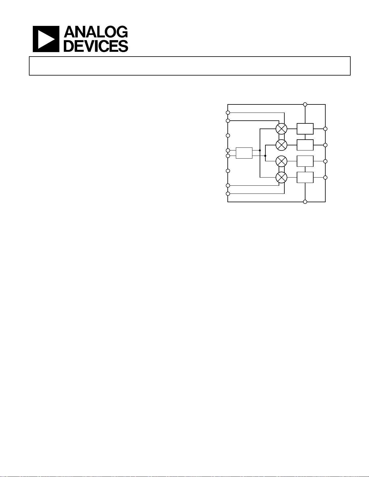
CH1
RF
ENABLE
LOC
OSC
RESET
CH2
RF
Phase Shifter
FUNCTIONAL BLOCK DIAGRAM
CH1
PHASE
SELECT
+
–
AD8333
÷4
+
–
0°
90°
90°
0°
Figure 1.
Φ
Φ
Φ
Φ
CH2
PHASE
SELECT
AD8333
I1
Q1
Q2
I2
05543-001
GENERAL DESCRIPTION
The AD8333 is a dual-phase shifter and I/Q demodulator that
enables coherent summing and phase alignment of multiple
analog data channels. It is the first solid-state device suitable for
beamformer circuits, such as those used in high performance
medical ultrasound equipment featuring CW Doppler. The RF
inputs interface directly with the outputs of the dual-channel,
low noise preamplifiers included in the
A divide-by-4 circuit generates the internal 0° and 90° phases
of the local oscillator (LO) that drive the mixers of a pair of
matched I/Q demodulators.
The AD8333 can be applied as a major element in analog
beamformer circuits in medical ultrasound equipment.
The AD8333 features an asynchronous reset pin. When used in
arrays, the reset pin sets all the LO dividers in the same state.
Sixteen discrete phase rotations in 22.5° increments can be
selected independently for each channel. For example, if CH1 is
used as a reference and the RF signal applied to CH2 has an I/Q
phase lead of 45°, CH2 can be phase aligned with CH1 by
choosing the correct code.
Rev. B
Information furnished by Analog Devices is believed to be accurate and reliable. However, no
responsibility is assumed by Anal og Devices for its use, nor for any infringements of patents or ot her
rights of third parties that may result from its use. Specifications subject to change without notice. No
license is granted by implication or otherwise under any patent or patent rights of Analog Devices.
Trademarks and registered trademarks are the property of their respective owners.
AD8332.
Phase shift is defined by the output of one channel relative to
another. For example, if the code of Channel 1 is adjusted to
0000 and that of Channel 2 to 0001 and the same signal is
applied to both RF inputs, the output of Channel 2 leads that
of Channel 1 by 22.5°.
The I and Q outputs are provided as currents to facilitate
summation. The summed current outputs are converted to
voltages by a high dynamic-range, current-to-voltage (I-V)
converter, such as the
AD8021, configured as a transimpedance
amplifier. The resultant signal is then applied to a high resolution
ADC, such as the
AD7665 (16 bit/570 kSPS).
The two I/Q demodulators can be used independently in other
nonbeamforming applications. In that case, a transimpedance
amplifier is needed for each of the I and Q outputs, four in total
for the dual I/Q demodulator.
The dynamic range is 161 dB/Hz at each I and Q output, but the
following transimpedance amplifier is an important element in
maintaining the overall dynamic range, and attention needs to
be paid to optimal component selection and design.
The AD8333 is available in a 32-lead LFCSP (5 mm × 5 mm)
package for the industrial temperature range of −40°C to +85°C.
One Technology Way, P.O. Box 9106, Norwood, MA 02062-9106, U.S.A.
Tel: 781.329.4700 www.analog.com
Fax: 781.461.3113 ©2005–2007 Analog Devices, Inc. All rights reserved.

AD8333
TABLE OF CONTENTS
Features .............................................................................................. 1
Applications....................................................................................... 1
Functional Block Diagram .............................................................. 1
General Description......................................................................... 1
Revision History ............................................................................... 2
Specifications..................................................................................... 3
Absolute Maximum Ratings............................................................ 5
ESD Caution.................................................................................. 5
Pin Configuration and Function Descriptions............................. 6
Equivalent Input Circuits ................................................................7
Typical Performance Characteristics............................................. 8
Test Circ uit s .....................................................................................14
Theory of Operation ...................................................................... 17
Quadrature Generation............................................................. 17
I/Q Demodulator and Phase Shifter........................................ 17
Dynamic Range and Noise........................................................ 18
Summation of Multiple Channels (Analog Beamforming).. 19
Phase Compensation and Analog Beamforming................... 19
Channel Summing ..................................................................... 20
Dynamic Range Inflation.......................................................... 22
Disabling the Current Mirror and Decreasing Noise............ 22
Applications..................................................................................... 24
Logic Inputs and Interfaces....................................................... 24
Reset Input .................................................................................. 24
Connecting to the LNA of the AD8331/
AD8332/AD8334/AD8335 VGAs............................................ 24
LO Input ...................................................................................... 25
Evaluation Board ........................................................................ 25
Outline Dimensions .......................................................................27
Ordering Guide .......................................................................... 27
REVISION HISTORY
5/07—Rev. A to Rev. B
Changes to Features and Figure 1................................................... 1
Changes to Table 1............................................................................ 3
Changes to Figure 41 to Figure 43................................................ 14
Changes to Figure 44 to Figure 47................................................ 15
Changes to Figure 48 to Figure 51................................................ 16
Changes to Figure 55...................................................................... 20
Changes to Evaluation Board Section.......................................... 25
Changes to Ordering Guide.......................................................... 27
5/06—Rev. 0 to Rev. A
Changes to Figure 62...................................................................... 26
10/05—Revision 0: Initial Version
Rev. B | Page 2 of 28

AD8333
SPECIFICATIONS
VS = ±5 V, TA = 25°C, 4 fLO = 20 MHz, fRF = 5.01 MHz, fBB = 10 kHz, PLO ≥ 0 dBm, single-ended, sine wave; per channel performance, dBm
(50 Ω), unless otherwise noted (see
Table 1.
Parameter Conditions Min Typ Max Unit
OPERATING CONDITIONS
LO Frequency Range
Square wave 0.01 200 MHz
Sine wave, see Figure 22 2 200 MHz
RF Frequency Range Mixing DC 50 MHz
Baseband Bandwidth Limited by external filtering DC 50 MHz
LO Input Level See Figure 22 0 13 dBm
V
(VS) ±4.5 ±5 ±6 V
SUPPLY
Temperature Range −40 +85 °C
DEMODULATOR PERFORMANCE
RF Differential Input Impedance 6.7||6.5 kΩ||pF
LO Differential Input Capacitance 0.6 pF
Transconductance
All phases 2.17 mS
Dynamic Range IP1dB, input referred noise (dBm) 159 dB/Hz
Maximum RF Input Swing Differential; inputs biased at 2.5 V; Pin RFxP and Pin RFxN 2.8 V p-p
Peak Output Current (No Filtering) 0° phase shift ±4.7 mA
45° phase shift ±6.6 mA
Input P1dB
Ref = 1 V
Third-Order Intermodulation (IM3) f
Equal Input Levels Baseband tones: −7 dBm @ 8 kHz and 13 kHz −75 dBc
Unequal Input Levels Baseband tones: −1 dBm @ 8 kHz and −31 dBm @ 13 kHz −77 dBc
Third-Order Input Intercept (IP3)
LO Leakage
Conversion Gain All codes, see Figure 41 4.7 dB
Input Referred Noise Output noise/conversion gain, see Figure 41 10 nV/√Hz
Output Current Noise Output noise ÷ 787 Ω 22 pA/√Hz
Noise Figure With AD8332 LNA
R
R
R
Bias Current Pin 4LOP and Pin 4LON −3 μA
Pin RFxP and Pin RFxN −70 μA
LO Common-Mode Voltage Range Pin 4LOP and Pin 4LON (each pin) 0.2 3.8 V
RF Common-Mode Voltage
Output Compliance Range Pin IxPO and Pin QxPO −1.5 +0.7 V
Figure 41).
4× internal LO at Pin 4LOP and Pin 4LON
Demodulated I
, each Ix or Qx output after low-pass
OUT/VIN
filtering measured from RF inputs
Ref = 50 Ω 14.5 dBm
RMS
= 5.010 MHz, f
RF1
Same conditions as IM3 30 dBm
= 5.015 MHz, fLO = 5.023 MHz
RF2
Measured at RF inputs, worst phase, measured into 50 Ω
1.5 dBV
<−97 dBm
(limited by measurement)
Measured at baseband outputs, worst phase, 8021 disabled,
−60 dBm
measured into 50 Ω
= 50 Ω, RFB = ∞ 7.8 dB
S
= 50 Ω, RFB = 1.1 kΩ 9.0 dB
S
= 50 Ω, RFB = 274 Ω 11.0 dB
S
For maximum differential swing; Pin RFxP and Pin RFxN
2.5 V
(dc-coupled to AD8332 LNA output)
Rev. B | Page 3 of 28

AD8333
Parameter Conditions Min Typ Max Unit
PHASE ROTATION PERFORMANCE One CH is reference, other is stepped
Phase Increment 16 phase steps per channel 22.5 Degrees
Quadrature Phase Error I1 to Q1 and I2 to Q2, 1σ −2 ±0.1 +2 Degrees
I/Q Amplitude Imbalance I1 to Q1 and I2 to Q2, 1σ ±0.05 dB
Channel-to-Channel Matching Phase match I1/I2 and Q1/Q2; −40°C < TA < 85°C ±1 Degrees
Amplitude match I1/I2 and Q1/Q2; −40°C < TA < 85°C ±0.25 dB
LOGIC INTERFACES
Logic Level High Pin PHxx, Pin RSET, and Pin ENBL 1.7 5 V
Logic Level Low Pin PHxx, Pin RSET, and Pin ENBL 0 1.3 V
Bias Current
Pin PHxx and Pin ENBL Logic high 10 40 90 μA
Logic low −30 −7 +10 μA
Pin RSET Logic high 50 120 180 μA
Logic low −70 −20 0 μA
Input Resistance Pin PHxx and Pin ENBL 60 kΩ
Pin RSET 20 kΩ
Reset Hold Time
Minimum Reset Pulse Width 300 ns
Reset Response Time See Figure 35 300 ns
Phase Response Time See Figure 38 5 μs
Enable Response Time See Figure 34 300 ns
POWER SUPPLY Pin VPOS and Pin VNEG
Supply Voltage ±4.5 ±5 ±6 V
Quiescent Current, All Phase Bits = 0 @ 25°C
Pin VPOS 38 44 51 mA
Pin VNEG −24 −20 −16 mA
Over Temperature −40°C < TA < 85°C
Pin VPOS, all phase bits = 0 40 54 mA
Pin VNEG −24 −19 mA
Quiescent Power Per channel, all phase bits = 0 170 mW
Per channel, any 0 or 1 combination of phase bits 190 mW
Disable Current All channels disabled
Pin VPOS 1.0 1.25 1.5 mA
Pin VNEG −300 −200 −100 μA
PSRR
Pin VPOS to Ix/Qx outputs (measured @ AD8021 output) −81 dB
Pin VNEG to Ix/Qx outputs (measured @ AD8021 output) −75 dB
Reset is asynchronous; clock disabled when RSET goes HI
until 300 ns after RSET goes LO; see
Figure 58
300 ns
Rev. B | Page 4 of 28
AD8333
ABSOLUTE MAXIMUM RATINGS
Table 2.
Parameter Rating
Voltages
Supply Voltage, V
RF Pins Input VS, GND
LO Inputs VS, GND
Code Select Inputs, V VS, GND
Thermal Data—4-Layer JEDEC Board No Air
Flow (Exposed Pad Soldered to PCB)
θ
JA
θ
JB
θ
JC
Ψ
JT
Ψ
JB
Maximum Junction Temperature 150°C
Maximum Power Dissipation
(Exposed Pad Soldered to PC Board)
Operating Temperature Range −40°C to +85°C
Storage Temperature Range −65°C to +150°C
Lead Temperature (Soldering, 60 sec) 300°C
S
6 V
41.0°C/W
23.6°C/W
4.4°C/W
0.4°C/W
22.4°C/W
1.5 W
Stresses above those listed under Absolute Maximum Ratings
may cause permanent damage to the device. This is a stress
rating only; functional operation of the device at these or any
other conditions above those indicated in the operational
section of this specification is not implied. Exposure to absolute
maximum rating conditions for extended periods may affect
device reliability.
ESD CAUTION
Rev. B | Page 5 of 28

AD8333
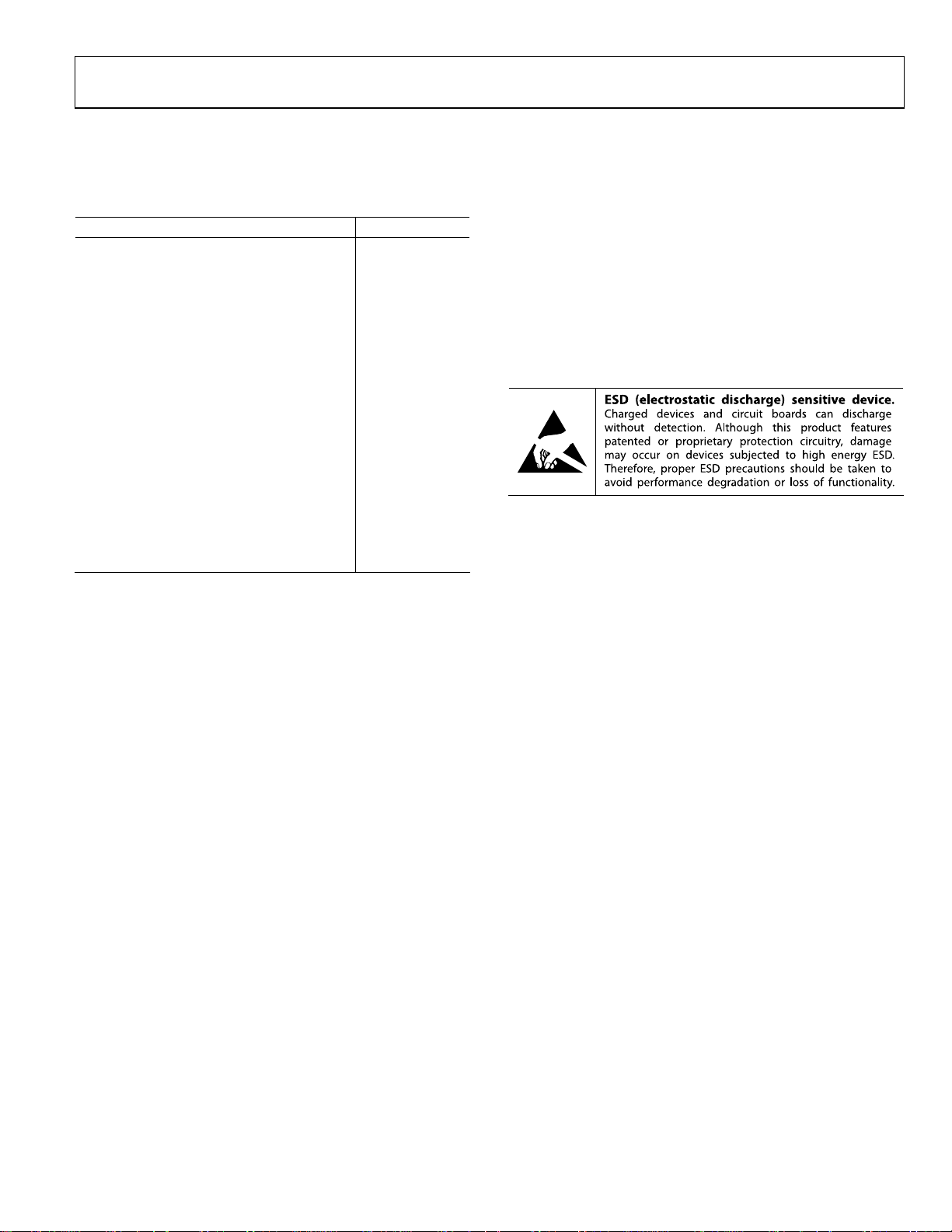
PIN CONFIGURATION AND FUNCTION DESCRIPTIONS
P
VPOS
PH11
32
RF1N
VPOS29RF1
PH10
31
30
ENBL25I1NO
28
27
26
PH12
PH13
COMM
4LOP
4LON
LODC
PH23
PH22
1
2
3
4
5
6
7
8
PIN 1
INDICATOR
AD8333
TOP VIEW
(Not to Scale)
9
11
0
PH2110PH2
VPOS
12
13
14
RF2P
RF2N
VPOS
24
I1PO
23
Q1PO
22
Q1NO
21
VNEG
20
COMM
19
Q2NO
18
Q2PO
17
I2PO
15
16
I2NO
RSET
05543-002
Figure 2. 32-Lead LFCSP Pin Configuration
Table 3. Pin Function Descriptions
Pin No. Mnemonic Description
1, 2,
7, 8
PH12, PH13
PH23, PH22
Quadrant Select LSB, MSB. Binary code. These logic inputs select the quadrant: 0° to 90°, 90° to180°,
180° to 270°, 270° to 360° (see Table 4 ). Logic threshold is at about 1.5 V and therefore can be driven by
3 V CMOS logic (see
Figure 3).
3, 20 COMM Ground. These two pins are internally tied together.
4, 5 4LOP, 4LON
LO Inputs. No internal bias; therefore, these pins need to be biased by external circuitry. For optimum
performance, these inputs should be driven differentially with a signal level that is not less than what is
shown in
correctly (see
Figure 22. Bias current is only −3 μA. Single-ended drive is also possible if the inputs are biased
Figure 4).
6 LODC Decoupling Pin for LO. A 0.1 μF capacitor should be connected between this pin and ground (see Figure 5).
9, 10,
31, 32
11, 14,
27, 30
PH21, PH20
PH10, PH11
VPOS
Phase Select LSB, MSB. Binary code. These logic inputs select the phase for a given quadrant: 0°, 22.5°, 45°, 67.5°
(see
Table 4). Logic threshold is at about 1.5 V and therefore can be driven by 3 V CMOS logic (see Figure 3).
Positive Supply. These pins should be decoupled with a ferrite bead in series with the supply, plus a 0.1 μF and
100 pF capacitor between the VPOS pins and ground. Because the VPOS pins are internally connected, one set
of supply decoupling components for all four pins should be sufficient.
12, 13,
28, 29
15 RSET
16, 19,
22, 25
17, 18,
23, 24
21 VNEG
RF2P, RF2N
RF1N, RF1P
I2NO, Q2NO
Q1NO, I1NO
I2PO, Q2PO
Q1PO, I1PO
RF Inputs. These pins are biased internally; however, it is recommended that they be biased by dc coupling to
the output pins of the
differential swing is 2.5 V if ±5 V supplies are used (see
AD8332 LNA. The optimum common-mode voltage for maximum symmetrical input
Figure 6).
Reset for Divide-by-4 in LO Interface. Logic threshold is at about 1.5 V and therefore can be driven by
3 V CMOS logic (see
Figure 3).
Negative I/Q Outputs. These outputs are not connected for normal usage but can be used for filtering if needed.
Together with the positive I/Q outputs, they allow bypassing the internal current mirror if a lower noise output
circuit is available; VNEG needs to be tied to GND to disable the current mirror (see
Figure 7).
Positive I/Q Outputs. These outputs provide a bidirectional current that can be converted back to a voltage via
a transimpedance amplifier. Multiple outputs can be summed together by simply connecting them together.
The bias voltage should be set to 0 V or less by the transimpedance amplifier (see
Figure 7).
Negative Supply. This pin should be decoupled with a ferrite bead in series with the supply, plus a 0.1 μF and
100 pF capacitor between the pin and ground.
26 ENBL Chip Enable. Logic threshold is at about 1.5 V and therefore can be driven by 3 V CMOS logic (see Figure 3).
Rev. B | Page 6 of 28
AD8333
4
EQUIVALENT INPUT CIRCUITS
VPOS
VPOS
4LOP
LON
PHxx
ENBL
RSET
COMM
Figure 3. Logic Inputs
VPOS
COMM
Figure 4. Local Oscillator Inputs
VPOS
LOGIC
INTERFACE
05543-003
05543-004
RFxP
RFxN
COMM
05543-006
Figure 6. RF Inputs
COMM
IxNO
QxNO
IxPO
QxPO
VNEG
05543-007
Figure 7. Output Drivers
LODC
COMM
Figure 5. LO Decoupling Pin
05543-005
Rev. B | Page 7 of 28
AD8333
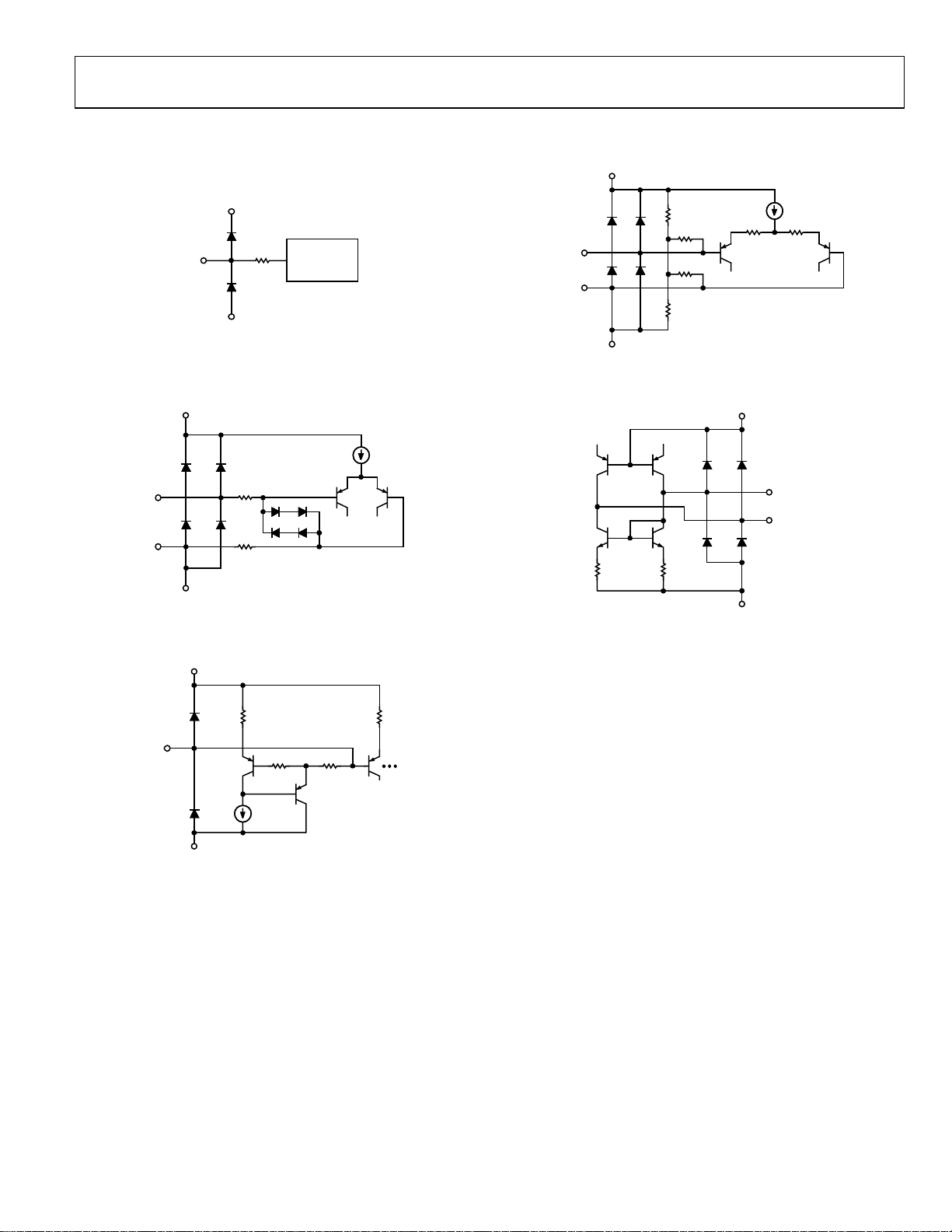
TYPICAL PERFORMANCE CHARACTERISTICS
VS = ±5 V, TA = 25°C, 4fLO = 20 MHz, fLO = 5 MHz, fRF = 5.01 MHz, fBB = 10 kHz, PLO ≥ 0 dBm (50 Ω); single-ended sine wave;
per channel performance, differential voltages, dBm (50 Ω), phase select code = 0000, unless otherwise noted (see
1.5
1.0
0.5
0
–0.5
IMAGINARY (Normalized)
–1.0
–1.5
–2.0
f = 1MHz
Q
I
CODE 1000
CODE 1100
–1.5 –1.0 –0.5 0 0.5 1.0 1.5
REAL (Normalized)
CODE 0100
CODE 0011
CODE 0010
CODE 0001
CODE 0000
2.0
Figure 8. Normalized Vector Plot of Phase, CH2 with Respect to CH1;
CH1 Is Fixed at 0°, CH2 Stepped 22.5°/Step, All Codes Displayed
360
1MHz
315
5MHz
270
05543-008
2
f = 5MHz
1
0
–1
–2
2
f = 1MHz
1
PHASE ERROR (Degrees)
0
–1
–2
0000
0010 0100 0110 1000 1010 1100 1110
CODE (Binary)
Figure 11. Phase Error of CH2 with Respect to CH1 vs.
Code at 1 MHz and 5 MHz
500mV
Figure 41).
1111
05543-011
225
180
135
PHASE (Degrees)
90
45
0
0000
0010 0100 0110 1000 1010 1100 1110
CODE (Binary)
1111
Figure 9. Phase of CH2 with Respect to CH1 vs. Code at 1 MHz and 5 MHz
1.0
f = 5MHz
0.5
0
–0.5
–1.0
1.0
f = 1MHz
0.5
AMPLITUDE ERROR (dB)
0
–0.5
–1.0
0000
0010 0100 0110 1000 1010 1100 1110
CODE (Binary)
1111
Figure 10. Amplitude Error of CH2 with Respect to CH1 vs.
Code at 1 MHz and 5 MHz
05543-009
05543-010
20µs
05543-012
Figure 12. I or Q Output of CH2 with Respect to CH1, First Quadrant Shown
7
CHANNEL 1, I OUTPUT SHOWN
6
CODE 0000
CODE 0001
CODE 0010
CODE 0011
5
GAIN (dB)
4
3
1M
RF FREQUENCY (Hz)
10M
50M
05543-013
Figure 13. Conversion Gain vs. RF Frequency, First Quadrant,
Baseband Frequency = 10 kHz
Rev. B | Page 8 of 28
AD8333
2.0
1.5
1.0
0.5
0
–0.5
–1.0
–1.5
QUADRATURE PHASE ERROR (Degrees)
–2.0
1M
10M
RF FREQUENCY (Hz)
100M
Figure 14. Representative Range of Quadrature Phase Errors vs.
RF Frequency, CH1 or CH2, All Codes
2.0
1.5
1.0
0.5
0
–0.5
–1.0
–1.5
QUADRATURE PHASE ERROR (Degrees)
–2.0
100
1k 10k
BASEBAND FREQUENCY (Hz)
100k
Figure 15. Range of Quadrature Phase Error vs. Baseband Frequency,
Figure 43)
10M
50M
I/Q AMPLITUDE IMBALANCE (dB)
0.5
0.4
0.3
0.2
0.1
–0.1
–0.2
–0.3
–0.4
–0.5
CH1 and CH2 ( see
0
1M
RF FREQUENCY (Hz)
Figure 16. Representative Range of Amplitude Imbalance of I/Q vs.
RF Frequency, CH1 or CH2, All Codes
05543-014
05543-015
05543-016
0.5
0.4
0.3
0.2
0.1
0
–0.1
–0.2
–0.3
I/Q AMPLITUDE IMBALANCE (dB)
–0.4
–0.5
100
1k 10k
BASEBAND FREQUENCY (Hz)
100k
Figure 17. Representative Range of I/Q Amplitude Imbalance vs.
10M
Figure 43)
fBB = 10kHz
I2/I1 DISPLAYED
50M
Baseband Frequency, CH1 and CH2 ( see
2.0
CODE 0000
–40°C
1.5
+25°C
+85°C
1.0
CODE 0001
–40°C
+25°C
0.5
+85°C
0
CODE 0010
–0.5
–40°C
+25°C
+85°C
AMPLITUDE ERROR (dB)
–1.0
CODE 0011
–40°C
–1.5
+25°C
+85°C
–2.0
1M
RF FREQUENC Y (Hz)
Figure 18. Typical I2/I1 or Q2/Q1 Amplitude Match vs. RF Frequency
First Quadrant, at Three Temperatures
PHASE ERROR (Degrees)
8
CODE 0000
–40°C
+25°C
6
+85°C
CODE 0001
–40°C
4
+25°C
+85°C
2
0
–2
fBB= 10kHz
I2/I1 DISPLAYED
–4
1M
CODE 0010
–40°C
+25°C
+85°C
CODE 0011
–40°C
+25°C
+85°C
RF FREQUE NCY (Hz)
10M 50M
Figure 19. I2/I1 or Q2/Q1 Phase Error vs. RF Frequency,
Baseband Frequency = 10 kHz, at Three Temperatures
05543-017
05543-018
05543-043
Rev. B | Page 9 of 28

AD8333
C
2.8
CHANNEL 1, I OUTPUT SHOWN
TRANSCONDUC TANCE = [(V
2.7
2.6
CODE 0000
CODE 0001
2.5
CODE 0010
CODE 0011
TANCE (ms)
2.4
2.3
2.2
TRANSCONDU
2.1
2.0
1M
RF FREQUENCY (Hz)
/787Ω)VRF]
BB
10M
Figure 20. Transconductance vs. RF Frequency, First Quadrant
10
0
–10
–20
–30
–40
GAIN (dB)
–50
–60
–70
–80
–20
f = 5MHz
GAIN = V
BB/VRF
CODE 0000
CODE 0001
CODE 0010
CODE 0011
–15 –10 –5
POWER (dBm)
Figure 21. Conversion Gain vs. LO Level, First Quadrant
5
ALL CODES
0
–5
–10
–15
–20
–25
MINIMUM LO LEVEL (dBm)
–30
–35
–40
100k
1M 10M
FREQUENCY (Hz)
REGION OF USEABLE
LO LEVELS
Figure 22. Minimum LO Level vs. RF Frequency, Single-Ended,
Sine Wave LO Drive to Pin 4LOP or Pin 4LON
50M
0
100M
05543-020
05543-021
05543-022
10
GAIN (dB)
GAIN = VBB/V
5
0
–5
–10
–15
–20
–25
–30
0
0.51.01.52.02.53.03.54.04.5
RF
+85°C
+25°C
–40°C
COMMON-MODE VOLTAGE (V)
Figure 23. LO Common-Mode Range at Three Temperatures
20
18
16
14
12
10
8
IP1dB (dBm)
6
4
2
0
1M
RF FREQUENCY (Hz)
10M
Figure 24. IP1dB vs. Frequency, Baseband Frequency = 10 kHz,
IM3 (dBc)
–10
–20
–30
–40
–50
–60
–70
–80
–90
0
1M
First Quadrant (see
–7dBm
3 8 13 18
IM3 PRODUCTS
LO = 5.023MHz
RF1 = 5.015MHz
RF2 = 5.010MHz
RF FREQUENCY (Hz)
BOTH CHANNELS
Figure 42)
10M
Figure 25. Representative Range of IM3 vs. RF Frequency,
First Quadrant (see
Figure 49)
5.0
50M
50M
05543-019
05543-023
05543-024
Rev. B | Page 10 of 28

AD8333
40
BOTH CHANNELS
35
30
25
20
OIP3 (dBm)
15
10
5
0
1M
RF FREQUENCY (Hz)
10M
Figure 26. Representative Range of OIP3 vs. RF Frequency,
Figure 49)
10k
35
30
25
20
15
OIP3 (dBm)
10
5
0
1k
First Quadrant (see
CHANNEL 1 RF
CHANNEL 2 RF
BASEBAND FREQUENCY (Hz)
Figure 27. OIP3 vs. Baseband Frequency (see
0
LO LEVEL = 0dBm
–10
–20
–30
–40
–50
LO LEAKAGE (dBm)
–60
–70
–80
1M
Q1
Q2
I1
I2
RF FREQUENCY (Hz)
10M
Figure 28. LO Leakage vs. RF Frequency at Baseband Outputs
Figure 48)
50M
100k
50M
05543-025
05543-026
05543-027
0
LO LEVEL = 0dBm
–20
–40
LO LEAKAGE (dBm)
–60
–80
–100
–120
–140
1M
RF1P
RF2P
RF1N
RF2N
10M
RF FREQUENCY (Hz)
Figure 29. LO Leakage vs. RF Frequency at RF Inputs
16 –142.9
14 –144.1
I1
Q1
12 –145.4
10 –147.0
8 –148.9
6 –151.4
NOISE (nV/ Hz)
4 –154.9
2 –161.0
0
1M
RF FREQUENCY (Hz)
10M
50M
Figure 30. Input Referred Noise vs. RF Frequency
20
18
16
14
12
10
8
NOISE FIGURE (dB)
6
4
2
0
1M
RF FREQUENCY (Hz)
10M 50M
Figure 31. Noise Figure vs. RF Frequency with AD8332 LNA
50M
05543-028
NOISE (dBm)
05543-029
05543-064
Rev. B | Page 11 of 28

AD8333
172
170
168
166
164
162
160
158
DYNAMIC RANGE (dB)
156
154
152
Figure 32. Dynamic Range vs. RF Frequency, IP1dB Minus Noise Level,
GAIN (dB)
I1
Q1
I1 + I2
Q1 + Q2
1M
RF FREQUENCY (Hz)
10M
Single Channel and Two Channels Summed
6
4
2
0
–2
–4
GAIN = VBB/V
CODE 0000
CODE 0010
2V
200ns
05543-046
50M
500mV
05543-030
Figure 35. Reset Response—Top: Signal at Reset Pin
Bottom: Output Signal (see
5V
RF
Figure 45)
–6
–8
–10
–3.0
–2.5 –2.0 –1.5 –1.0 –0.5 0 0.5
VOLTAGE (V)
Figure 33. Output Compliance Range (IxPO, QxPO) (see
500mV
200ns2V
Figure 34. Enable Response—Top: Enable Signal
Bottom: Output Signal (see
Figure 44)
1.0
Figure 50)
05543-045
05543-044
1V 1V
40µs
Figure 36. Phase Switching Response—CH2 Leads CH1 by 45°,
Top: Input to PH21, Select Code = 0010
Red: Ref CH1 IOUT; Gray: CH2 IOUT Phase Shifted 45°,
CH1 Ref Phase Select Code = 0000
5V
1V 1V
40µs
Figure 37. Phase Shifting Response—CH2 Leads CH1 by 90°,
Top: Input to PH21, Select Code = 0100
Red: Ref CH1 IOUT, Gray: CH2 IOUT Phase Shifted 90°,
CH1 Ref Phase Code = 0000
05543-047
05543-048
Rev. B | Page 12 of 28

AD8333
5V
1V 1V 40µs
Figure 38. Phase Shifting Response—CH2 Leads CH1 by 180°,
Top: Input to PH23 Select Code = 1000
Red: Ref CH1 IOUT, Gray: CH2 IOUT Phase Shifted 180°,
CH1 Ref Phase Code = 0000
0
–10
–20
–30
–40
–50
PSRR (dB)
–60
VNEG
VPOS
–70
–80
–90
100k
Figure 39. PSRR vs. Frequency (see
1M 10M
FREQUENCY (Hz)
Figure 51)
05543-049
50M
05543-050
60
50
40
30
20
10
QUIESCENT SUPPLY CURRENT (mA)
0
–50
–30 –10 10 30 50 70
TEMPERATURE (°C)
VPOS
VNEG
05543-051
90
Figure 40. Quiescent Supply Current vs. Temperature
Rev. B | Page 13 of 28

AD8333
A
A
A
TEST CIRCUITS
D8021
787Ω
2.2nF
2.2nF
787Ω
AD8021
OSCILLOSCOPE
05543-032
LPF
50Ω
SIGNAL
GENERATOR
120nH
FB
0.1µF
0.1µF
AD8332
LNA
GENERATOR
20Ω
20Ω
SIGNAL
RFxP
IxxO
AD8333
RFxN Q xxO
4LOP
50Ω
Figure 41. Default Test Circuit
D8021
100Ω
10nF
10nF
100Ω
AD8021
OSCILLOSCOPE
05543-033
LPF
50Ω
SIGNAL
GENERATOR
120nH
FB
0.1µF
0.1µF
AD8332
LNA
GENERATOR
20Ω
20Ω
SIGNAL
RFxP
IxxO
AD8333
RFxN Q xxO
4LOP
50Ω
Figure 42. P1dB Test Circuit
D8021
1µF
1µF
AD8332
LNA
GENERATOR
20Ω
20Ω
SIGNAL
RFxP
IxxO
AD8333
RFxN QxxO
4LOP
50Ω
787Ω
787Ω
AD8021
OSCILLOSCOPE
05543-034
LPF
50Ω
SIGNAL
GENERATOR
120nH
FB
Figure 43. Phase and Amplitude vs. Baseband Frequency
Rev. B | Page 14 of 28

AD8333
A
A
A
A
D8021
1µF
1µF
AD8332
LNA
GENERATOR
20Ω
20Ω
50Ω
SIGNAL
RFxP
IxxO
AD8333
RFxN QxxO
4LOP
ENBL
50Ω
787Ω
787Ω
AD8021
SIGNAL
GENERATOR
OSCILLOSCOPE
05543-035
LPF
50Ω
SIGNAL
GENERATOR
120nH
FB
Figure 44. Enable Response
D8021
1µF
1µF
AD8332
LNA
GENERATOR
20Ω
20Ω
50Ω
SIGNAL
RFxP
IxxO
AD8333
RFxN QxxO
4LOP
RST
50Ω
787Ω
787Ω
AD8021
SIGNAL
GENERATOR
OSCILLOSCOPE
05543-036
LPF
50Ω
SIGNAL
GENERATOR
120nH
FB
Figure 45. Reset Response
0.1µF
D8332
LNA
20Ω
20Ω
RFxP IxxO
AD8333
RFxN QxxO
4LOP
OSCILLOSCOPE
50Ω 50Ω
LPF
50Ω
SIGNAL
GENERATOR
120nH
FB
0.1µF
50Ω
SIGNAL
GENERATOR
05543-037
Figure 46. RF Input Range
D8021
6.98kΩ
270pF
270pF
6.98kΩ
AD8021
SPECTRUM
ANALYZER
05543-052
0.1µF
RFxP
RFxN QxxO
SIGNAL
GENERATOR
IxxO
AD8333
4LOP
50Ω
Figure 47. Noise Test Circuit
Rev. B | Page 15 of 28

AD8333
A
A
A
A
D8021
SIGNAL
GENERATOR
50Ω
COMBINER
–6dB
50Ω
SIGNAL
GENERATOR
120nH
FB
0.1µF
0.1µF
AD8332
LNA
20Ω
RFxP
RFxN QxxO
20Ω
SIGNAL
GENERATOR
IxxO
AD8333
4LOP
50Ω
787Ω
100pF
100pF
787Ω
AD8021
SPECTRUM
ANALYZER
05543-053
Figure 48. OIP3 vs. Baseband Frequency
D8021
SIGNAL
GENERATOR
50Ω
COMBINER
–6dB
50Ω
SIGNAL
GENERATOR
120nH
FB
0.1µF
0.1µF
AD8332
LNA
20Ω
RFxP
RFxN QxxO
20Ω
SIGNAL
GENERATOR
IxxO
AD8333
4LOP
50Ω
787Ω
2.2nF
2.2nF
787Ω
AD8021
SPECTRUM
ANALYZER
05543-054
Figure 49. OIP3 and IM3 vs. RF Frequency
D8021
787Ω
2.2nF
2.2nF
787Ω
AD8021
OSCILL OSCOPE
05543-055
LPF
50Ω
SIGNAL
GENERATOR
120nH
FB
0.1µF
0.1µF
AD8332
LNA
20Ω
RFxP
RFxN QxxO
20Ω
SIGNAL
GENERATOR
IxxO
AD8333
4LOP
50Ω
Figure 50. Output Compliance Range
0.1µF
D8332
LNA
GENERATOR
20Ω
20Ω
SIGNAL
RFxP
IxxO
AD8333
RFxN QxxO
4LOP
50Ω
NETWORK
ANALYZER
05543-056
LPF
50Ω
SIGNAL
GENERATOR
120nH
FB
0.1µF
Figure 51. PSRR Test Circuit
Rev. B | Page 16 of 28

AD8333
C
THEORY OF OPERATION
The AD8333 is a dual I/Q demodulator with a programmable
phase shifter for each channel. The primary applications are
phased array beamforming in medical ultrasound, phased array
radar, and smart antennas for mobile communications. The
AD8333 can also be used in applications that require two wellmatched I/Q demodulators.
Figure 52 shows the block diagram and pinout of the AD8333.
Three analog and nine quasi-logic level inputs are required.
Two RF inputs accept signals from the RF sources and a local
oscillator (applied to the differential input pins marked 4LOx)
common to both channels comprise the analog inputs. Four
logic inputs per channel define one of 16 delay states/360° (or
22.5°/step) selectable with the PHx0 to PHx3. The reset input is
used to synchronize AD8333s used in arrays.
PH11
PH10
VPOS
RFIP
RFIN
VPOS
ENBL
I1NO
26
25
24
I1PO
23
Φ
Φ
Φ
Φ
15
16
RSET
Q1PO
22
Q1NO
21
VNEG
20
COMM
19
Q2NO
18
Q2PO
17
I2PO
I2NO
PH12
PH13
OMM
4LOP
4LON
LODC
PH23
PH22
1
CHANNEL 1
2
3
4
BUF
5
6
7
CHANNEL 2
8
32
31
Φ SEL
LOGIC
AD8333
÷4
Φ SEL
LOGIC
9
10
PH21
30
29
28
27
BIAS
0°
90°
90°
0°
11
12
13
14
POS
PH20
RF2P
POS
RF2N
Figure 52. Block Diagram and Pinout
Each of the current formatted I and Q outputs sum together for
beamforming applications. Multiple channels are summed and
converted to a voltage using a transimpedance amplifier. If
desired, channels can also be used individually.
QUADRATURE GENERATION
The internal 0° and 90° LO phases are digitally generated
by a divide-by-4 logic circuit. The divider is dc-coupled and
inherently broadband; the maximum LO frequency is limited
only by its switching speed. The duty cycle of the quadrature LO
signals is intrinsically 50% and is unaffected by the asymmetry
of the externally connected 4LOx inputs. Furthermore, the
divider is implemented such that the 4LOx signals reclock the
final flip-flops that generate the internal LO signals and thereby
minimizes noise introduced by the divide circuitry.
5543-057
For optimum performance, the 4LOx inputs are driven
differentially but can also be driven single ended. A good
choice for a drive is an LVDS device. The common-mode
range on each pin is approximately 0.2 V to 3.8 V with nominal
±5 V supplies.
The minimum LO level is frequency dependent (see
Figure 22).
For optimum noise performance, it is important to ensure that
the LO source has very low phase noise (jitter) and adequate
input level to assure stable mixer-core switching. The gain
through the divider determines the LO signal level vs. RF
frequency. The AD8333 can be operated to very low frequencies
at the LO inputs if a square wave is used to drive the LO.
Beamforming applications require a precise channel-to-channel
phase relationship for coherence among multiple channels. A
reset pin (RSET) is provided to synchronize the 4LOx divider
circuits when the AD8333s are used in arrays. The RSET pin
resets the counters to a known state after power is applied to
multiple AD8333s. A logic input must be provided to the RSET
pin when using more than one AD8333. See the
Reset Input
section for more details.
I/Q DEMODULATOR AND PHASE SHIFTER
The I/Q demodulators consist of double-balanced Gilbert cell
mixers. The RF input signals are converted into currents by
transconductance stages that have a maximum differential input
signal capability of 2.8 V p-p. These currents are then presented
to the mixers, which convert them to baseband: RF − LO and
RF + LO. The signals are phase shifted according to the code
applied to Pin PHx0 to Pin PHx3 (see
function is an integral part of the overall circuit (patent pending).
The phase shift listed in Column 1 of
between the baseband I or Q channel outputs. As an example,
for a common signal applied to the RF inputs of an AD8333, the
baseband outputs are in phase for matching phase codes.
However, if the phase code for Channel 1 is 0000 and that of
Channel 2 is 0001, Channel 2 leads Channel 1 by 22.5°.
Following the phase shift circuitry, the differential current
signal is converted from differential to single ended via a
current mirror. An external transimpedance amplifier is
needed to convert the I and Q outputs to voltages.
Table 4). The phase shift
Table 4 is defined as being
Rev. B | Page 17 of 28

AD8333
Table 4. Phase Select Code for Channel-to-Channel Phase Shift
φ-Shift
PHx3 PHx2 PHx1 PHx0
0° 0 0 0 0
22.5° 0 0 0 1
45° 0 0 1 0
67.5° 0 0 1 1
90° 0 1 0 0
112.5° 0 1 0 1
135° 0 1 1 0
157.5° 0 1 1 1
180° 1 0 0 0
202.5° 1 0 0 1
225° 1 0 1 0
247.5° 1 0 1 1
270° 1 1 0 0
292.5° 1 1
0 1
315° 1 1 1 0
337.5° 1 1 1 1
DYNAMIC RANGE AND NOISE
Figure 53 is an interconnection block diagram of the AD8333.
For optimum system noise performance, the RF input signal is
provided by a very low noise amplifier, such as the LNA of the
AD8332 or the preamplifier of the AD8335. In beamformer
applications, the I and Q outputs of a number of receiver
channels are summed (for example, the two channels illustrated
in
Figure 53). The dynamic range of the system increases by the
factor 10log
random uncorrelated noise.) The noise in the two channel
example of
doubles (6 dB), yielding an aggregate SNR improvement of
(6 − 3) = 3 dB.
(N), where N is the number of channels (assuming
10
Figure 53 is increased by 3 dB while the signal
R
TRANSMITTER
TRANSDUCER
CLOCK
GENERATOR
TRANSMITTER
TRANSDUCER
T/R
SW
T/R
SW
FB
AD8333
÷4
R
FB
AD8332 LNA OR
AD8335 PREAMP
CH1
RF
0°
90°
90°
0°
CH2
RF
AD8332 LNA OR
AD8335 PREAMP
Figure 53. Interconnection Block Diagram
2
2
PHASE
SELECT
2
2 2
2 2
2 2
PHASE
SELECT
CH1
4
4
CH2
Judicious selection of the RF amplifier ensures the least
degradation in dynamic range. The input referred spectral
voltage noise density (e
) of the AD8333 is nominally 9 nV/√Hz
n
to 10 nV/√Hz. For the noise of the AD8333 to degrade the
system noise figure (NF) by 1 dB, the combined noise of the
source and the LNA should be about twice that of the AD8333
or 18 nV/√Hz. If the noise of the circuitry before the AD8333 is
<18 nV/√Hz, the system NF degrades more than 1 dB. For
example, if the noise contribution of the LNA and source is
equal to the AD8333, or 9 nV/√Hz, the degradation is 3 dB. If
the circuit noise preceding the AD8333 is 1.3× as large as that of
the AD8333 (or about 11.7 nV/√Hz), the degradation is 2 dB.
For a circuit noise 1.45× that of the AD8333 (13.1 nV/√Hz),
degradation is 1.5 dB.
To determine the input referred noise, it is important to know
the active low-pass filter (LPF) values R
FILT
and C
Figure 53. Typical filter values (for example, those used on the
evaluation board) are 787 Ω and 2.2 nF and implement a
90 kHz single-pole LPF. If the RF and LO are offset by 10 kHz,
the demodulated signal is 10 kHz and is passed by the LPF. The
single-channel mixing gain, from the RF input to the
output (for example, I1´, Q1´) is approximately 1.7 × 4.7 dB.
This together with the 9 nV/√Hz AD8333 noise results in about
15.3 nV/√Hz at the
AD8021 output. Because the AD8021,
including the 787 Ω feedback resistor, contributes another
4.4 nV/√Hz, the total output referred noise is about 16 nV/√Hz.
This value can be adjusted by increasing the filter resistor while
maintaining the corner frequency, thereby increasing the gain.
The factor limiting the magnitude of the gain is the output
swing and drive capability of the op amp selected for the I-to-V
converter, in this instance the
2
Φ
Φ
Φ
Φ
I1
Q1
Q2
I2
*UP TO 8 CHANNELS
PER AD8021
*
*
C
FILT
R
FILT
AD8021
C
FILT
R
FILT
AD8021
AD8021.
ΣI
ADC 16-BIT
570kSPS
AD7665
AD7686
ΣQ
ADC 16-BIT
570kSPS
IDATA
OR
QDATA
, shown in
FILT
AD8021
05543-038
Rev. B | Page 18 of 28

AD8333
SUMMATION OF MULTIPLE CHANNELS (ANALOG BEAMFORMING)
Beamforming, as applied to medical ultrasound, is defined as
the phase alignment and summation of signals generated from a
common source but received at different times by a multielement
ultrasound transducer. Beamforming has two functions: it imparts
directivity to the transducer, enhancing its gain, and it defines a
focal point within the body from which the location of the
returning echo is derived. The primary application for the
AD8333 is in analog beamforming circuits for ultrasound.
PHASE COMPENSATION AND ANALOG BEAMFORMING
Modern ultrasound machines used for medical applications
employ a 2
typical array sizes of 16 or 32 receiver channels phase-shifted
and summed together to extract coherent information. When
used in multiples, the desired signals from each of the channels
can be summed to yield a larger signal (increased by a factor N,
where N is the number of channels), while the noise is increased
by the square root of the number of channels. This technique
enhances the signal-to-noise performance of the machine. The
critical elements in a beamformer design are the means to align
the incoming signals in the time domain, and the means to sum
the individual signals into a composite whole.
In traditional analog beamformers incorporating Doppler, a
V-to-I converter per channel and a crosspoint switch precede
passive delay lines used as a combined phase shifter and
summing circuit. The system operates at the receive frequency
(RF) through the delay line, and then the signal is downconverted by a very large dynamic range I/Q demodulator.
The resultant I and Q signals are filtered and sampled by two
high resolution ADCs. The sampled signals are processed to
extract the relevant Doppler information.
n
binary array of receivers for beamforming, with
Alternatively, the RF signal can be processed by downconversion
on each channel individually, phase shifting the downconverted
signal, and then combining all channels. The AD8333 provides
the means to implement this architecture. The downconversion
is done by an I/Q demodulator on each channel, and the summed
current output is the same as in the delay line approach. The
subsequent filters after the I-to-V conversion and the ADCs
are similar.
The AD8333 integrates the phase shifter, frequency conversion,
and I/Q demodulation into a single package and directly yields
the baseband signal. To illustrate,
Figure 54 is a simplified
diagram showing two channels. The ultrasound wave USW
is received by two transducer elements, TE1 and TE2, in an
ultrasound probe and generates signals E1 and E2. In this
example, the phase at TE1 leads the phase at TE2 by 45°.
TRANSDUCER
ELEMENTS TE1
AND TE2
CONVERT USW TO
USW AT TE1
LEADS USW
AT TE2 BY
ELECTRICAL
SIGNALS
ES1 LEADS
45°
Figure 54. Simplified Example of the AD8333 Phase Shifter
45°
ES2 BY 45°
AD8332
19dB
LNA
E1
E2
19dB
LNA
AD8333
PHASE BIT
SETTINGS
CH 1 REF
(NO PHASE
LEAD)
CH 2
PHASE
LEAD 45°
S1 AND S2
ARE NOW IN
PHASE
S1
S2
SUMMED
OUTPUT
S1 + S2
In a real application, the phase difference depends on the
element spacing, λ (wavelength), speed of sound, angle of
incidence, and other factors. The signals ES1 and ES2 are
amplified 19 dB by the low noise amplifiers in the AD8332.
For optimum signal-to-noise performance, the output of the
LNA is applied directly to the input of the AD8333. To sum the
signals ES1 and ES2, ES2 is shifted 45° relative to ES1 by setting
the phase code in Channel 2 to 0010. The phase-aligned current
signals at the output of the AD8333 are summed in an I-to-V
converter to provide the combined output signal with a
theoretical improvement in dynamic range of 3 dB for the
sum of two channels.
05543-063
Rev. B | Page 19 of 28

AD8333
CHANNEL SUMMING
In a beamformer using the AD8333, the bipolar currents at the I
and Q outputs are summed directly.
summed channels (for clarity shown as current sources) as an
example of an active current summing circuit using the AD8333,
AD8021s as first-order current summing circuits, and AD797s
as low noise second-order summing circuits. Beginning with
the op amps, there are a few important considerations in the
circuit shown in
Figure 55.
The op amps selected for the first-order summing amplifiers
must have good frequency response over the full operating
frequency range of the AD8333s and be able to source the
current required at the AD8333 I and Q outputs.
The total current of each of the AD8333s is 6.6 mA for the
multiples of the 45° phase settings (Code 0010, Code 0110,
Code 1010, and Code 1110) and divided about equally between
the baseband frequencies (including a dc component) and the
second harmonic of the local oscillator frequency. The desired
CW signal tends to be much less (<40 dB) than the unwanted
interfering signals. When determining the large signal
EIGHT AD8333 I OR Q OUTPUTS ,
(IF THE PHASE SETT ING IS 45°)
3.3mA AT DC + 3.3mA AT 2LO
Figure 55 illustrates 16
6.6mA PEAK EACH
(SAME AS ABOVE)
FIRST ORDER
SUMMING AMPLIFIERS
2
3
2
3
Figure 55. A 16-Channel Beamformer
–
ΣA
+
–
ΣB
+
C1A
18nF
R1A
100Ω
0.1µF
0.1µF
C1B
18nF
R1B
100Ω
0.1µF
0.1µF
requirements of the first-order summing amplifiers and lowpass filters, the very small CW signal can be ignored. The
number of channels that can be summed is limited by the
output drive current capacity of the op amp selected: 60 mA
to 70 mA for a linear output current for ±5 V and ±12 V,
respectively, for the
AD8021. Because the AD8021 implements
an active LPF together with R1x and C1x, it must absorb the
worst-case current provided by the AD8333, for example,
6.6 mA. Therefore, the maximum number of channels that the
AD8021 can sum is 10 for ±12 V or eight for ±5 V supplies.
In practical applications, CW channels are used in powers of
two, thus the maximum number per
AD8021 is eight.
Another consideration for the op amp selected as an I-to-V
converter is the compliance voltage of the AD8333 I and Q
outputs. The maximum compliance voltage is 0.5 V, and a dc
bias must be provided at these pins. The
AD8021 active LPF
satisfies these requirements; it keeps the outputs at 0 V via the
virtual ground at the op amp inverting input while providing
any needed dc bias current.
LPF1A
88kHz
+2.8V BASEBAND
SIGNAL
LPF2A
HPF1A
AD8021
AD8021
+5V
–5V
+5V
–5V
C2A
1µF
C2B
1µF
R2A
698Ω
R2B
698Ω
100Hz
81kHz
R3A
698Ω
C3A
5.6nF
SUMMING AMPLIFIER
R3B
698Ω
C3B
5.6nF
SECOND ORDER
R4
0.1µF
2
–
AD797
3
+
0.1µF
+10V
–10V
05543-058
Rev. B | Page 20 of 28

AD8333
F
As previously noted, a typical CW signal has a large dc and
very low frequency component compared to its desired low CW
Doppler baseband frequency, and another unwanted component
at the 2 × LO. The dc component flows through the gain resistors
R1x, while the 2 × LO flows through the capacitors C1x. The
smaller desired CW Doppler baseband signal is in the frequency
range of 1 kHz to 50 kHz.
Because the output current of the AD8333 contains the baseband
frequency, a dc component, and the 2 × LO frequency voltages,
the desired small amplitude baseband signal must be extracted
after a series of filters. These are shown in
Figure 55 as LPFn,
HPFn, and gain stages.
Before establishing the value of C
, the resistor R
LPF1
LPF1
is
selected based on the peak operating current and the linear
range of the op amp. Because the peak current for each AD8333
is 6.6 mA and there are eight channels to be summed, the total
peak current required is 52.8 mA. Approximately half of this
current is dc and the other half at a frequency of 2 × LO. Therefore,
about 26.4 mA flows through the resistor while the remaining
26.4 mA flows through the capacitor. R1 was selected as 100 Ω
and, after filtering, generates a peak dc and very low frequency
voltage of 2.64 V at the
AD8021 output. For power supplies of
±5 V, 100 Ω is a good choice for R1.
However, because the CW signal needs to be amplified as
much as possible and the noise degradation of the signal path
minimized, the value of R1 should be as large as possible. A
larger supply helps in this regard, and the only factor limiting
the largest supply voltage is the required power.
For a ±10 V supply on the
AD8021, R1 can be increased to
301 Ω and realize the same headroom as with a ±5 V supply. If a
higher value of R1 is used, C1 must be adjusted accordingly (in
this example 1/3 the value of the original value) to maintain the
desired LPF roll-off. The principal advantage of a higher supply
is greater dynamic range, and the trade-off is power consumption.
The user must weigh the trade-offs associated with the supply
voltage, R1, C1, and the following circuitry. A suggested design
sequence is:
• Select a low noise, high speed op amp. The spectral density
noise (e
) should be <2 nV/√Hz and the 3 dB BW ≥ 3 × the
n
expected maximum 2 × LO frequency.
• Divide the maximum linear output current by 6.6 mA to
determine the maximum number of AD8333 channels that
can be summed.
• Select the largest value of R1 that permits the output voltage
swing within the power supply rails.
• Calculate the value of C1 to implement the LPF corner that
allows the CW Doppler signal to pass with maximum
attenuation of the 2 × LO signal.
The filter LPF1 establishes the upper frequency limit of the
baseband frequency and is selected well below the 2 × LO
frequency, typically 100 kHz or less, or, as an example, 88 kHz
as shown in
Figure 55.
A useful equation for calculating C1 is
1
1
C =
(1)
12π
fR
1
LP
As previously mentioned, the AD8333 output current contains a
dc current component. This dc component is converted to a
large dc voltage by the
AD8021 LPF. Capacitor C2 filters this dc
component and, with R2 + R3, establishes a high-pass filter with
a low frequency cutoff of about 100 Hz. Capacitor C3 is much
smaller than C2 and, consequently, can be neglected. C2 can be
calculated by
2
=
1
(2)
)32(2π
fRRC+
1
HPF
To achieve maximum attenuation of the 2 × LO frequency, a
second low-pass filter, LPF2, is established using the parallel
combination of R2 and R3, and C3. Its −3 dB frequency is
f
= (3)
2
LPF
In the example shown in
1
()
33||22π
CRR
Figure 55, f
= 81 kHz.
LPF2
Finally, the feedback resistor of the AD797 must be calculated.
This is a function of the input current (number of channels)
and the supply voltage.
The second-order summing amplifier requires a very low noise
op amp, such as the
AD797, with 0.9 nV/√Hz, because the
amplifier gain is determined by Feedback Resistor R4 divided
by the parallel combination of the LPF2 resistors seen looking
back toward the
AD8021s. Referring to Figure 55, the AD797
inband (100 Hz to 88 kHz) gain is expressed as
R4
[]
The
AD797 noise gain can increase to unacceptable levels
++
(4)
)(||)( R2BR2BR3AR2A
because the denominator of the gain equation is the parallel
resistance of all the R2 + R3 resistors in the
AD8021 outputs.
For example, for a 64-channel beamformer, the resistance seen
looking back toward the
AD8021s is about 1.4 k/8 = 175 .
For this reason, the value of (R2x + R3x) should be as large as
possible to minimize the noise gain of the
this is the case for the
AD8021 stages because they look back
AD797. (Note that
into the high impedance current sources of the AD8333s.)
Due to these considerations, it is advantageous to increase the
gain of the
AD8021s as much as possible because the value of
(R2x + R3x) can be increased proportionally. Resistors (R2x +
R3x) convert the CW voltages to currents that are summed at
the inverting inputs of the
AD797 op amp and amplified and
converted to voltages by R4.
Rev. B | Page 21 of 28

AD8333
The value of R4 needs to be chosen iteratively as follows:
• Determine the number of AD8021 first-order summing
amplifiers. In
Figure 55, there are two; for a 32-channel
beamformer, there would be four, and for a 64-channel
beamformer, there would be eight.
Determine the output noise after the AD8021s. A first-order
•
calculation can be based on a value of AD8333 output
current noise of about 20 pA/√Hz. For the values in
Figure 55,
this results is about 6 nV/√Hz for eight channels after the
AD8021s. Adding the noise of the AD8021 and the 100
feedback resistor results in about 6.5 nV/√Hz total noise after
AD8021 LPF in the CW Doppler band.
the
Determine the noise of the circuitry after the AD797 and the
•
desired signal level.
Determine the voltage and current noise of the second-order
•
summing amplifiers.
Choose a value for R2x + R3x and for R4. Determine the
•
resulting output noise after the
AD797 for one channel and
then multiply by the square root of the number of summed
AD8021s. Next, check AD797 output noise (both current and
voltage noise). Ideally, the sum of the noise of the resistors
and the
the
Check the following stages output noise against the
•
AD797 is less than a factor-of-3 than the noise due to
AD8021 outputs.
calculated noise from the combiner circuit and AD8333s;
ideally the noise from the following stage should be less than
1/3 of the calculated noise.
If the combined noise is too large, experiment with
•
increasing/decreasing values for R2x + R3x and R4.
To simplify, the user can also simulate or build a combiner
circuit for optimum performance. It should be noted that the
~20 pA/√Hz out of the AD8333 is for the AD8333 with shorted
RF inputs. In an actual system, the current noise out of the
AD8333 is most likely dominated by the noise from the AD8332
LNA and the noise from the source and other circuitry before
the LNA. This helps ease the design of the combiner. The
preceding procedures for determining the optimum values for
the combiner are based on the noise floor of the AD8333 only.
As an example, for a 32-channel beamformer using four lowpass filters, as shown in
Figure 55, (R2x + R3x) = 1.4 k and
R4 = 6.19 kΩ. The theoretical noise increase of √N is degraded
by only about 1 dB.
DYNAMIC RANGE INFLATION
Although all 64 channels could theoretically be summed
together at a single amplifier, it is important to realize that the
dynamic range of the summed output increases by 10 × log
if all channels have uncorrelated noise, where
N is the number
of channels to be summed.
10
(N)
The summed signal level increases by a factor of N while the
noise increases only as √N. In the case of 64 channels, this is an
increase in dynamic range of 18 dB. Note that the AD8333
dynamic range is already about 160 dB/Hz; the summed
dynamic range is 178 dB/Hz (equivalent to about 29.5 b/Hz).
In a 50 kHz noise bandwidth, this is 131 dB (21.7 bits).
DISABLING THE CURRENT MIRROR AND DECREASING NOISE
The noise contribution of the AD8333 can potentially be
reduced if the current mirrors that convert the internal
differential signals to single ended are bypassed (see
Current mirrors interface to the
in
Figure 53, and output capacitors across the positive and negative
outputs provide low-pass filtering. The
AD8021 I-V converters shown
AD8021s force the
AD8333 output voltage to 0 V and process the bipolar output
current; however, the internal current mirrors introduce a
significant amount of noise. This noise can be reduced if they
are disabled and the outputs externally biased.
The mirrors are disabled by connecting VNEG to ground and
providing external bias networks, as shown in
larger the drop across the resistors, the less noise they contribute to
the output; however, the voltage on the IxxO and QxxO nodes
cannot exceed 0.5 V. Voltages exceeding approximately 0.7 V
turn on the PNP devices and forward bias the ESD protection
diodes. Inductors provide an alternative to resistors, enabling
reduced static power by eliminating the power dissipation in the
bias resistors.
COMM
OTHER
CHANNELS
IxNO
QxNO
IxPO
QxPO
1
VNEG
1
NOTE THAT PIN VNEG AND PIN COMM
ARE CONNECTED TOGETHER.
Figure 56. Bypassing the Internal Current Mirrors
With inductors, the main limitation might be low frequency
operation, as is the case in CW Doppler in ultrasound where
the frequency range of interest goes from a few hundred Hertz
to about 30 kHz. In addition, it is still important to provide
enough gain through the I-to-V circuitry to ensure that the bias
resistor and I-to-V converter noise do not contribute significantly
to the noise from the AD8333 outputs. Another approach could
be to provide a single external current mirror that combines all
channels; it would also be possible to implement a high-pass
filter with this circuit to help with offset and low frequency
reduction.
Figure 56).
Figure 56. The
I-V
I-V
05543-039
Rev. B | Page 22 of 28

AD8333
The main disadvantage of the external bias approach is that now
two I-V amplifiers are needed because of the differential output
Figure 56). For beamforming applications, the outputs
(see
would still be summed as before, but now there is twice the
number of lines. Only two bias resistors are needed for all
outputs that are connected together. The resistors are scaled by
dividing the value of a single output bias resistor through N,
the number of channels connected in parallel. The bias current
depends on the phase selected: for phase 0°, this is about
2.5 mA per side, while in the case of 45°, this is about 3.5 mA
per side. The bias resistors should be chosen based on the
larger bias current value of 3.5 mA and the chosen VNEG.
VNEG should be at least −5 V and can be larger for additional
noise reduction.
Excessive noise or distortion at high signal levels degrades the
dynamic range of the signal. Transmitter leakage and echoes
from slow moving tissue generate the largest signal amplitudes
in ultrasound CW Doppler mode and are largest near dc and at
low frequencies. A high-pass filter introduced immediately
following the AD8333 reduces the dynamic range. This is
shown by the two coupling capacitors after the external bias
resistors in
in their particular application. Care must be taken in designing
the external circuitry to avoid introducing noise via the external
bias and low frequency reduction circuitry.
Figure 56. Users have to determine what is acceptable
Rev. B | Page 23 of 28

AD8333
T
R
T
R
t
t
APPLICATIONS
The AD8333 is the key component of a phase-shifter system
that aligns time-skewed information contained in RF signals.
Combined with a variable gain amplifier (VGA) and low noise
amplifier (LNA), the AD8333 forms a complete analog receiver
for a high performance ultrasound system.
Figure 57 is a block
diagram of a complete receiver using the AD8333 and the
AD8332 family.
FROM
RANSDUCE
T/R SWITCH
FROM
RANSDUCE
T/R SWITCH
LNA1
LNA2
AD8333
I1
16-BIT
Q1
ADC
I2
16-BIT
ADC
Q2
HS ADC
HS ADC
PROCESSOR
PROCESSOR
PROCESSOR
PROCESSOR
AD8332
Figure 57. Block Diagram—Ultrasound Receiver Using the AD8333
and AD8332 LNA
As a major element of an ultrasound system, it is important to
consider the many I/O options of the AD8333 necessary to
perform its intended function.
Figure 61 shows the basic
connections.
LOGIC INPUTS AND INTERFACES
The logic inputs of the AD8333 are all bipolar-level sensitive
inputs. They are not edge triggered, nor are they to be confused
with classic TTL or other logic family input topologies. The
voltage threshold for these inputs is VPOS × 0.3, so for a 5 V
supply the threshold is 1.5 V, with a hysteresis of ±0.2 V.
Although the inputs are not of themselves logic inputs, any 5 V
logic family can drive them.
RESET INPUT
The RSET pin is used to synchronize the LO dividers in
AD8333 arrays. Because they are driven by the same internal
LO, the two channels in any AD8333 are inherently synchronous.
However, when multiple AD8333s are used, it is possible that
their dividers wake up in different phase states. The function of
the RSET pin is to phase align all the LO signals in multiple
AD8333s.
The 4 × LO divider of each AD8333 can initiate in one of four
possible states: 0°, 90°, 180°, or 270°. The internally generated
I/Q signals of each AD8333 LO are always at a 90° angle relative
to each other, but a phase shift can occur during power-up
between the internal LOs of the different AD8333s.
05543-059
The RSET pin provides an asynchronous reset of the LO
dividers by forcing the internal LO to hang. This mechanism
also allows the measurement of nonmixing gain from the RF
input to the output.
The rising edge of the active high RSET pulse can occur at any
time; however, the duration must be ≥ 300 ns minimum (t
PW-MIN
).
When the RSET pulse transitions from high to low, the LO
dividers are reactivated; however, there is a short delay until the
divider recovers to a valid state. To guarantee synchronous
operation of an array of AD8333s, the 4 LO clock must be
disabled when the RSET transitions high and remain disabled
for at least 300 ns after RSET transitions low.
4×LO
t
RSET
THE TIMING OF THE RISING
EDGE OF RSET IS NOT
CRITICAL AS LONG AS THE
t
PW-MIN
=HOLDTIME
HOLD
= MINIMUM PULSE WIDTH
PW-MIN
t
PW-MIN
IS SATISFIED
HOLD
05543-060
Figure 58. Timing of the RSET Signal to 4 LO
Synchronization of multiple AD8333s can be checked as
follows:
Set the phase code of all AD8333 channels the same, for
•
example, 0000.
Apply a test signal to a single channel that generates a sine
•
wave in the baseband output and measure the output.
•
Apply the same test signal to all channels simultaneously and
measure the output.
Since all the phase codes of the AD8333s are the same, the
•
combined signal should be N times bigger than the single
channel. The combined signal is less than N times one channel if
any of the LO phases of individual AD8333s are in error.
CONNECTING TO THE LNA OF THE AD8331/ AD8332/AD8334/AD8335 VGAs
+5V
AD8332
LNA
Figure 59. Connecting the AD8333 to the LNA of an AD8332
The RFxx inputs (Pin 12, Pin 13, Pin 28, and Pin 29) are
optimized for maximum dynamic range when dc-coupled to
the differential output pins of the LNA of the
AD8334
directly, as shown in
or the AD8335 series of VGAs and can be connected
Figure 59.
RFxP
AD8333
RFxN
–5V
05543-061
AD8331/AD8332/
Rev. B | Page 24 of 28

AD8333
V
V
If amplifiers other than the AD8332 LNA are connected to the
input, attention must be paid to their bias and drive levels. For
maximum input signal swing, the optimum bias level is 2.5 V,
and the RF input must not exceed 5 V to avoid turning on the
ESD protection circuitry. If ac coupling is used, a bias circuit,
such as that illustrated in
Figure 60, is recommended. An
internal bias network is provided; however, additional external
biasing can center the RF input at 2.5 V.
+5
5.23kΩ
1.4kΩ
AD8333
RFxP
RFxN
–5V
05543-062
RF IN
3.74kΩ
0.1µF
0.1µF
1.4kΩ
Figure 60. AC Coupling the AD8333 RF Input
RF IN
PHASE
+5V
31.6kΩ
PHASE
RF IN
–
+
1
PH12 I1PO
2
PH13 Q1PO
3
COMM Q1NO
4
4LOP VNEG
5
4LON COMM
0.1µF
6
LODC Q2NO
7
PH23
8
PH22
+
–
Figure 61. AD8333 Basic Connections
CHANNEL 1
CHANNEL 1
SELECT BI TS
*
33.2kΩ 33.2kΩ
0.1µF
+
LOCAL
OSC
0.1µF
–
31.6kΩ
CHANNEL 2
SELECT BI TS
CHANNEL 2
*OPTIONAL BIAS NETWORK. THESE COMPONENTS
MAY BE DELETED IF THE LO IS DC-COUPLED FROM
AN LVDS SOURCE BIASED AT 1.2V.
32
PH11
PH21
9
31
10
LO INPUT
The LO input is a high speed, fully differential, analog input
that responds to differences in the input levels (and not logic
levels). The LO inputs can be driven with a low common-mode
voltage amplifier, such as the National Semiconductor
DS90C401 LVDS driver.
The graphs shown in
Figure 22 and Figure 23 show the range of
common-mode voltages and useable LO levels when the LO
input is driven with a single-ended sine wave. Logic families,
such as TTL or CMOS, are unsuitable for direct coupling to
the LO input.
EVALUATION BOARD
Figure 62 is the evaluation board schematic. Consult the
AD8333-EVAL data sheet for further details.
POS
30
29
28
27
26
RFIP
PH10
RFIN
VPOS
VPOS
AD8333
PH2011VPOS12RF2P13RF2N14VPOS15RSET
RESET
INPUT
120nH FB
25
ENBL
I2NO
16
I1N0
Q2PO
I2PO
VPOS
24
23
22
21
20
19
18
17
+5V
0.1µF
CHANNEL 1
+ I OUT
CHANNEL 1
+ Q OUT
120nH FB
CHANNEL 2
+ Q OUT
CHANNEL 2
+ I OUT
0.1µF
0.1µF
–5V
05543-040
Rev. B | Page 25 of 28

AD8333
Q1
0Ω
R33
6
C29
2.2nF
–
1
27
–5VS
C28
5pF
5
A2
4
AD8021
+
3
8
0.1µF
C47
–5V
L4
C48
0.1µF
120nH FB
R41
787Ω
0.1µF
+5VS
C49
C36
0.1µF
0.1µF
R5
OPT
R39
I1
–5V
0Ω
R32
L7
C26
787Ω
2.2nF
–
27
120nH FB
5pF
C27
6
5
A1
4
AD8021
+
3
1
8
R40
787Ω
–5VS
C45
0.1µF
C46
+5VS
R3
+5VS
C44
–5V
+5V
0.1µF
L6
120nH FB
–5V
C8
C7
+5VS
10µF
10V
+
TP6
TP5
10µF
10V
SW15
L3
120nH FB
C24
0.1µF
242023
25
26
2730 29 28
+
+5V
SW5
SW6
VPOS
31
SW7
SW8
PH11 I1N0
32
R4
OPT
22
21
191718
I2PO
Q1PO
Q1NO
VNEG
COMM
I2PO
Q2PO
Q2NO
ENBL
VPOS
RFIN
RFIP
VPOS
AD8333
PH10
PH12
2
4LOP
PH13
3
4LON
COMM
6
514
PH22
LODC
PH23
8
7
C31
0Ω
Q2
0Ω
R35
–5VS
R42
2.2nF
6
5
A3
AD8021
+
–
1
8
27
R2
0Ω
+5VS
787Ω
C30
5pF
C50
0.1µF
4
3
+5V
R15
C41
OPT
0.1µF
RST
VPOS
I2NO
RSET
SW23
VPOS
RF2N
RF2P
VPOS
PH20
SW12
SW11
9101112131415 16
PH21
SW13
I2
0Ω
R38
C32
6
2.2nF
–
1
27
–5VS
C33
5pF
5
C52
A4
AD8021
8
0.1µF
4
+
3
+5VS
C51
0.1µF
+5VS
TP8
TP7
+5V
SW14
C17
C43
20
AD8332
514
C5
0.1µF
R1
1nF
19
NC
VOL2
100Ω
Z3
17
18
C13
VOH2
COMM
0.1µF
RCLMP
GAIN
MODE
VCM2
13 14 15 16
VIN2
VIP2
COM2
910 1112
7
VPS2
VPS
LOP2
LON2
8
R10
274Ω
C40
0.018µF
LMD2
INH2
6
0.1µF
GND1 GND2 GND3 GND4
R26
R25
20Ω
20Ω
L5 120nH FB
+5V
C42
0.1µF
21
22
23
24
VOL1
VPSV
VOH1
COMM
ENBV
VPS
ENBL
HILO
VCM1
VPS1
VPS
Z1
LMD1
INH1
3
C14
0.1µF
R9
274Ω
VIN1
29
VIP1
30
COM1
3132 28 252627
LOP1
LON1
2
R7
1.5kΩ
R13
2
4
C9
3
49.9Ω
LOP
0.1µF
DS90C401
R6
3.48kΩ
1
+5V
C12
0.1µF
C11
0.1µF
R22
R23
20Ω
20Ω
7
6
5
8
Z3 SPARE
C39
0.018µF
C2
C1
0.1µF
TP4
L1
C6
22pF
0.1µF
TP3
C3
C4
22pF
0.1µF
TP1
TP2
L2
IN1
120nH FB
IN2
120nH FB
05543-042
Figure 62. AD8333 Evaluation Board Schematic
Rev. B | Page 26 of 28

AD8333
OUTLINE DIMENSIONS
0.08
(CP-32-2)
0.60 MAX
25
24
EXPOSED
PAD
(BOTTOM VIEW)
17
16
3.50 REF
PIN 1
32
1
8
9
INDICATOR
3.25
3.10 SQ
2.95
0.25 MIN
THE EXPOSE PAD IS NOT CONNECTED
INTERNALLY. FOR I NCREASED RELIABILITY
OF THE SOL DER JOINTS AND MAXIMUM
THERMAL CAPABIL ITY IT IS RECOMMENDED
THAT THE PAD BE SOLDERED TO
THE GROUND PLANE.
041806-A
5.00
PIN 1
INDICATOR
1.00
0.85
0.80
12° MAX
SEATING
PLANE
BSC SQ
TOP
VIEW
0.80 MAX
0.65 TYP
0.30
0.23
0.18
4.75
BSC SQ
0.20 REF
COMPLIANT TO JEDEC STANDARDS MO-220-VHHD-2
0.05 MAX
0.02 NOM
0.60 MAX
0.50
BSC
0.50
0.40
0.30
COPLANARIT Y
Figure 63. 32-Lead Lead Frame Chip Scale Package [LFCSP_VQ]
5 mm × 5 mm Body, Very Thin Quad
Dimensions shown in millimeters
ORDERING GUIDE
Model Temperature Range Package Description Package Option
AD8333ACPZ
AD8333ACPZ-REEL
AD8333ACPZ-REEL7
AD8333ACPZ-WP
AD8333-EVALZ
1
Z = RoHS Compliant Part.
2
WP = Waffle pack.
1
1
1, 2
1
−40°C to +85°C 32-Lead Lead Frame Chip Scale Package [LFCSP_VQ] CP-32-2
−40°C to +85°C 32-Lead Lead Frame Chip Scale Package [LFCSP_VQ] CP-32-2
1
−40°C to +85°C 32-Lead Lead Frame Chip Scale Package [LFCSP_VQ] CP-32-2
−40°C to +85°C 32-Lead Lead Frame Chip Scale Package [LFCSP_VQ] CP-32-2
Evaluation Board
Rev. B | Page 27 of 28

AD8333
NOTES
©2005–2007 Analog Devices, Inc. All rights reserved. Trademarks and
registered trademarks are the property of their respective owners.
D05543-0-5/07(B)
Rev. B | Page 28 of 28
 Loading...