

Low Cost DC-150 MHz
Variable Gain Amplifier
FEATURES
Fully Differential Signal Path
May also be Used with Single-Sided Signals
Inputs from 0.3 mV to 1 V rms, Rail-to-Rail Outputs
Differential R
= 1 k; R
IN
(Each Output) 75
OUT
Automatic Offset Compensation (Optional)
Linear-in-dB and Linear-in-Magnitude Gain Modes
0 dB to 50 dB, for 0 V < V
< 1.5 V (30 mV/dB)
DBS
Inverted Gain Mode: 50 dB to 0 dB at –30 mV/dB
0.03 to 10 Nominal Gain for 15 mV < V
MAG
< 5 V
Constant Bandwidth: 150 MHz at All Gains
Low Noise: 5 nV/√Hz Typical at Maximum Gain
Low Distortion: ≤–62 dBc Typ
Low Power: 20 mA Typ at V
of 2.7 V – 6 V
S
Available in Space-Saving 3 3 LFCSP Package
APPLICATIONS
Pre-ADC Signal Conditioning
75 Cable Driving Adjust
AGC Amplifiers
GENERAL DESCRIPTION
The AD8330 is a wideband variable gain amplifier for use in
applications requiring a fully differential signal path, low noise, welldefined gain, and moderately low distortion, from dc to 150 MHz.
The input pins can also be driven from a single ended source. The
peak differential input is ±2V, allowing sine wave operation at
1V rms with generous headroom. The output pins can optionally
drive single-sided loads and each swing essentially rail-to-rail.
The differential output resistance is 150 Ω. The output swing is
a linear function of the voltage applied to the VMAG pin, which
internally defaults to 0.5 V, to provide a peak output of ±2 V.
This may be raised to 10 V p-p, limited by the supply voltage.
The basic gain function is linear-in-dB, controlled by the voltage
applied to pin VDBS. The gain ranges from 0 dB to 50 dB for
control voltages between 0 V and 1.5 V—a slope of 30 mV dB.
The gain linearity is typically within ±0.1 dB. By changing the
logic level on pin MODE, the gain will decrease over the same
range, with opposite slope. A second gain control port is provided
at pin VMAG and allows the user to vary the numeric gain from a
factor of 0.03 to 10. All the parameters of the AD8330 have low
sensitivities to temperature and supply voltages.
Using V
, the basic 0 dB to 50 dB range can be repositioned to any
MAG
value from 20 dB higher (that is, 20 dB to 70 dB) to at least 30 dB
lower (that is, –30 dB to +20 dB) to suit the application, providing
an unprecedented gain range of over 100 dB. A unique aspect of
the AD8330 is that its bandwidth and pulse response are essentially
constant for all gains, not only over the basic 50 dB linear-in-dB
*Protected by U.S.Patent No. 5,969,657; other patents pending.
REV. B
Information furnished by Analog Devices is believed to be accurate and
reliable. However, no responsibility is assumed by Analog Devices for its
use, nor for any infringements of patents or other rights of third parties that
may result from its use. No license is granted by implication or otherwise
under any patent or patent rights of Analog Devices. Trademarks and
registered trademarks are the property of their respective owners.
AD8330
*
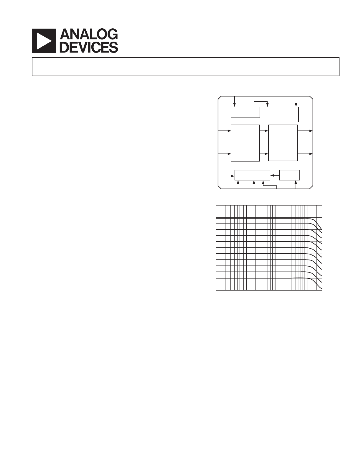
FUNCTIONAL BLOCK DIAGRAM
16 15 14 13
OFSTENBL CNTRVPOS
1
VPSI
INHI
2
INLO
3
MODE
4
90
70
50
30
10
GAIN – dB
–10
–30
–50
100k
BIAS AND V
VDBS CMGN VMAG
5678
REF
VGA CORE
GAIN INTERFACE
1M 10M 100M 300M
FREQUENCY – Hz
CM AND
OFFSET
CONTROL
OUTPUT
STAGES
OUTPUT
CONTROL
COMM
VPSO
OPHI
OPLO
CMOP
12
11
10
9
Figure 1. AC Response over the Extended Gain Range
range, but also when using the linear-in-magnitude function. The
exceptional stability of the HF response over the gain range is of
particular value in those VGA applications where it is essential
to maintain accurate gain law-conformance at high frequencies.
An external capacitor at pin OFST sets the high-pass corner of an
offset reduction loop, whose frequency may be as low as 5 Hz.
When this pin is grounded, the signal path becomes dc-coupled.
When used to drive an ADC, an external common-mode control
voltage at pin CNTR can be driven to within 0.5 V of either
ground or V
to accommodate a wide variety of requirements. By
S
default, the two outputs are positioned at the midpoint of the
supply, V
/2. Other features, such as two levels of power-down
S
(fully off and a hibernate mode), further extend the practical
value of this exceptionally versatile VGA.
The AD8330 is available in 16-lead LFCSP and 16-lead QSOP
packages and is specified for operation from –40°C to +85°C.
One Technology Way, P.O. Box 9106, Norwood, MA 02062-9106, U.S.A.
Tel: 781/329-4700 www.analog.com
Fax: 781/326-8703 © 2004 Analog Devices, Inc. All rights reserved.

AD8330–SPECIFICATIONS
(VS = 5 V, TA = 25C, CL = 12 pF on OPHI and OPLO, RL = 0/C, V
V
MAG
= 0/C, V
= 0 V, Differential Operation, unless otherwise noted.)
OFST
= 0.75 V, V
DBS
MODE
= HI,
Parameter Conditions Min Typ Max Unit
INPUT INTERFACE Pins INHI, INLO
Full-Scale Input V
= 0 V, Differential Drive ±1.4 ± 2V
DBS
V
= 1.5 V ±4.5 ± 6.3 mV
DBS
Input Resistance Pin-to-Pin 800 1k 1.2k Ω
Input Capacitance Either Pin to COMM 4 pF
Voltage Noise Spectral Density f = 1 MHz, V
= 1.5 V; 5 nV/√Hz
DBS
Inputs ac-shorted
Common-Mode Voltage Level 3.0 V
Input Offset Pin OFST Connected to COMM 1 mV rms
Drift 2 µV/°C
Permissible CM Range
1
0V
S
V
Common-Mode AC Rejection f = 1 MHz, 0.1 V rms –60 dB
f = 50 MHz –55 dB
OUTPUT INTERFACE Pins OPHI, OPLO
Small Signal –3 dB Bandwidth 0 V < V
Peak Slew Rate V
DBS
< 1.5 V 150 MHz
DBS
= 0 1500 V/µs
Peak-to-Peak Output Swing ±1.8 ± 2 ± 2.2 V
≥ 2 V (Peaks are Supply Limited) ±4 ±4.5 V
V
MAG
Common-Mode Voltage Pin CNTR O/C 2.4 2.5 2.6 V
Voltage Noise Spectral Density f = 1 MHz, V
Differential Output Impedance Pin-to-Pin 120 150 180 Ω
HD2
HD3
2
2
V
= 1 V p-p, f = 10 MHz, RL = 1 kΩ –62 dBc
OUT
V
= 1 V p-p, f = 10 MHz, RL = 1 kΩ –53 dBc
OUT
= 0 62 nV/√Hz
DBS
OUTPUT OFFSET CONTROL Pin OFST
AC-Coupled Offset C
High-Pass Corner Frequency C
on Pin OFST (0 V< V
HPF
= 3.3 nF, from OFST 100 kHz
HPF
to CNTR (Scales as 1/C
< 1.5 V) 10 mV rms
DBS
)
HPF
COMMON-MODE CONTROL Pin CNTR
Usable Voltage Range 0.5 4.5 V
Input Resistance From Pin CNTR to VS/2 4 kΩ
DECIBEL GAIN CONTROL Pins VDBS, CMGN, MODE
Normal Voltage Range CMGN Connected to COMM 0 to 1.5 V
Elevated Range CMGN O/C (V
Rises to 0.2 V) 0.2 to 1.7 V
CMGN
Gain Scaling Mode HIGH or LOW 27 30 33 mV/dB
Gain Linearity Error 0.3 V ≤ V
Absolute Gain Error V
= 0 –2 ± 0.5 +2 dB
DBS
≤ 1.2 V –0.35 ± 0.1 +0.35 dB
DBS
Bias Current Flows out of pin VDBS 100 nA
Incremental Resistance 100 MΩ
Gain Settling Time to 0.5 dB Error V
Stepped from 0.05 V–1.45 V 250 ns
DBS
or 1.45 V–0.05 V
Mode Up/Down Pin MODE
Mode Up Logic Level Gain Increases with V
Mode Down Logic Level Gain Decreases with V
, MODE = O/C 1.5 V
DBS
DBS
0.5 V
LINEAR GAIN INTERFACE Pins VMAG, CMGN
Peak Output Scaling, Gain vs. V
Gain Multiplication Factor vs. V
See Circuit Description Section 3.8 4.0 4.2 V/V
MAG
Gain is Nominal when V
MAG
= 0.5 V ⫻2
MAG
Usable Input Range 0 5 V
Default Voltage V
O/C 0.48 0.5 0.52 V
MAG
Incremental Resistance 4kΩ
Bandwidth For V
≥ 0.1 V 150 MHz
MAG
REV. B–2–

AD8330
Parameter Conditions Min Typ Max Unit
CHIP ENABLE Pin ENBL
Logic Voltage for Full Shutdown 0.5 V
Logic Voltage for Hibernate Mode Output Pins Remain at CNTR 1.3 1.5 1.7 V
Logic Voltage for Full Operation 2.3 V
Current in Full Shutdown 20 100 µA
Current in Hibernate Mode 1.5 mA
Minimum Time Delay
POWER SUPPLY Pins VPSI, VPOS, VPSO,
Supply Voltage 2.7 6 V
Quiescent Current V
NOTES
1
The use of an input common-mode voltage significantly different than the internally set value is not recommended due to its effect on noise performance.
See Figure 13.
2
See Typical Performance Characteristics for more detailed information on distortion in a variety of operating conditions.
3
For minimum sized coupling capacitors.
3
1.7 µs
COMM, CMOP
= 0.75 V 20 27 mA
DBS
REV. B
–3–
AD8330
ABSOLUTE MAXIMUM RATINGS
1
Supply Voltage . . . . . . . . . . . . . . . . . . . . . . . . . . . . . . . . . . . 6 V
Power Dissipation
RQ Package
2
. . . . . . . . . . . . . . . . . . . . . . . . . . . . . . 0.62 W
CP Package . . . . . . . . . . . . . . . . . . . . . . . . . . . . . . . .1.67 W
Input Voltage at Any Pin . . . . . . . . . . . . . . . . . . . V
+ 200 mV
S
Storage Temperature . . . . . . . . . . . . . . . . . . . –65°C to +105°C
JA
RQ-16 Package . . . . . . . . . . . . . . . . . . . . . . . . . 105.4°C/W
CP-16 Package . . . . . . . . . . . . . . . . . . . . . . . . . . . . . 60°C/W
JC
RQ-16 Package . . . . . . . . . . . . . . . . . . . . . . . . . . . . 39°C/W
ORDERING GUIDE
Model Temperature Range Package Description Package Option Branding
AD8330ACP-R2 –40°C to +85°C LFCSP CP-16-3 JFA
AD8330ACP-REEL –40°C to +85°C LFCSP CP-16-3 JFA
AD8330ACP-REEL7 –40°C to +85°C LFCSP CP-16-3 JFA
AD8330ACPZ-R2* –40°C to +85°C LFCSP CP-16-3 JFA
AD8330ACPZ-REEL* –40°C to +85°C LFCSP CP-16-3 JFA
AD8330ACPZ-REEL7*
–40°C to +85°C LFCSP CP-16-3 JFA
AD8330ARQ –40°C to +85°C QSOP RQ-16
AD8330ARQ-REEL –40°C to +85°C QSOP RQ-16
AD8330ARQ-REEL7 –40°C to +85°C QSOP RQ-16
AD8330ARQZ* –40°C to +85°C QSOP RQ-16
AD8330ARQZ-REEL* –40°C to +85°C QSOP RQ-16
AD8330ARQZ-REEL7*
–40°C to +85°C QSOP RQ-16
AD8330-EVAL Evaluation Board
*Z = Pb-free part.
Operating Temperature Range . . . . . . . . . . . . –40°C to +85°C
Lead Temperature (Soldering 60 sec) . . . . . . . . . . . . . . 300°C
NOTES
1
Stresses above those listed under Absolute Maximum Ratings may cause
permanent damage to the device. This is a stress rating only and functional
operation of the device at these or any other conditions above those indicated
in the operational section of this specification is not implied. Exposure to absolute
maximum rating conditions for extended periods may affect device reliability.
2
Four-Layer JEDEC Board (252P).
CAUTION
ESD (electrostatic discharge) sensitive device. Electrostatic charges as high as 4000 V readily
accumulate on the human body and test equipment and can discharge without detection. Although the
AD8330 features proprietary ESD protection circuitry, permanent damage may occur on devices
subjected to high energy electrostatic discharges. Therefore, proper ESD precautions are
recommended to avoid performance degradation or loss of functionality.
REV. B–4–
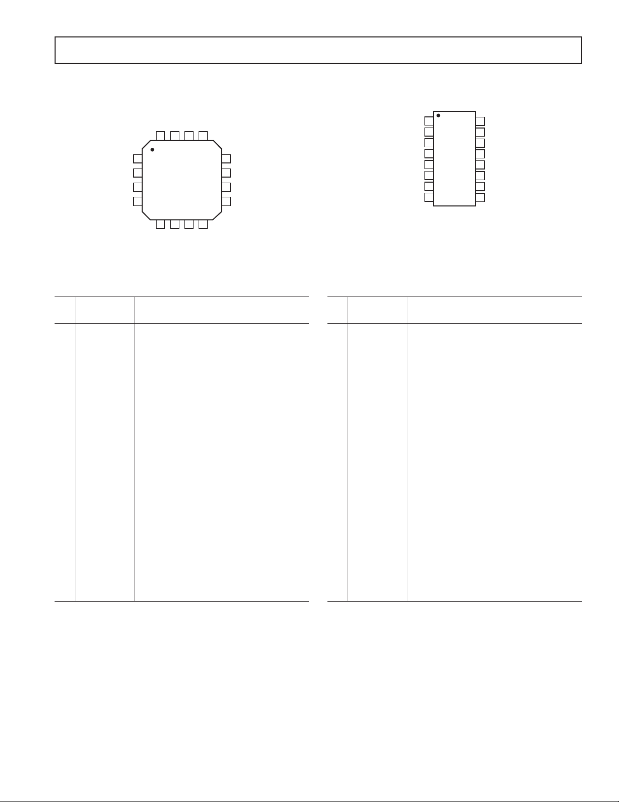
16-Lead LFCSP
AD8330
PIN CONFIGURATIONS
16-Lead QSOP
ENBL
OFST
VPOS
14
CMGN
13
COMM
CNTR
VMAG
12
11
10
9
VPSO
OPHI
OPLO
CMOP
VSPI
INHI
INLO
MODE
16
1
2
3
4
5678
VDBS
15
AD8330
TOP VIEW
(Not to Scale)
PIN FUNCTION DESCRIPTIONS
16-Lead LFCSP
Pin
No. Mnemonic Description
1 VPSI Positive Supply for Input Stages
2 INHI Differential Signal Input, Positive Polarity
3 INLO Differential Signal Input, Negative Polarity
4 MODE Logic Input: Selects Gain Slope. High =
Gain Up versus V
DBS
5 VDBS Input for Linear-in-dB Gain Control
Voltage, V
DBS
6 CMGN Common Baseline for Gain Control Interfaces
7 COMM Ground for Input and Gain Control Bias
Circuitry
8 VMAG Input for Gain/Amplitude Control, V
MAG
9 CMOP Ground for Output Stages
10 OPLO Differential Signal Output, Negative Polarity
11 OPHI Differential Signal Output, Positive Polarity
12 VPSO Positive Supply for Output Stages
13 CNTR Common-Mode Output Voltage Control
14 VPOS Positive Supply for Inner Stages
15 OFST Used in Offset Control Modes
16 ENBL Power Enable, Active High
1
OFST VPOS
2
ENBL CNTR
3
VPSI VPSO
INLO OPLO
MODE CMOP
VDBS VMAG
CMGN COMM
AD8330
4
INHI OPHI
TOP VIEW
(Not to Scale)
5
6
7
8
16
15
14
13
12
11
10
9
16-Lead QSOP
Pin
No. Mnemonic Description
1 OFST Used in Offset Control Modes
2 ENBL Power Enable, Active High
3 VPSI Positive Supply for Input Stages
4 INHI Differential Signal Input, Positive Polarity
5 INLO Differential Signal Input, Negative Polarity
6 MODE Logic Input: Selects Gain Slope. High =
Gain Up versus V
DBS
7 VDBS Input for Linear-in-dB Gain Control
Voltage, V
DBS
8 CMGN Common Baseline for Gain Control Interfaces
9 COMM Ground for Input and Gain Control Bias
Circuitry
10 VMAG Input for Gain/Amplitude Control, V
MAG
11 CMOP Ground for Output Stages
12 OPLO Differential Signal Output, Negative Polarity
13 OPHI Differential Signal Output, Positive Polarity
14 VPSO Positive Supply for Output Stages
15 CNTR Common-Mode Output Voltage Control
16 VPOS Positive Supply for Inner Stages
REV. B
–5–
AD8330–Typical Performance Characteristics
VS = 5 V, TA = 25C, CL = 12 pF, V
50
45
40
35
30
25
GAIN – dB
20
15
10
5
0
0 0.25 0.50 1.00 1.25 1.50
TPC 1. Gain vs. V
10
9
8
7
6
5
4
3
2
GAIN MULTIPLICATION FACTOR
1
0
01 345
= 0.75 V, V
DBS
0.75
V
DBS
2
V
MAG
– V
– V
= High (or O/C) V
MODE
HI MODELO MODE
DBS
= O/C, RL = O/C, V
MAG
= 0, Differential Operation, unless otherwise stated.
OFST
2.0
NORMALIZED @ V
1.5
1.0
0.5
10, 50MHz
0
–0.5
GAIN ERROR – dB
1MHz
–1.0
–1.5
–2.0
0 0.2 0.8 1.2 1.6
100MHz
0.4
TPC 4. Gain Error vs. V
20
2340 UNITS
MODE = LO
15
10
5
0
–30.6–30.5 –30.4 –30.3–30.2 –30.1–30.0 –29.9–29.8 –29.7–29.6 –29.5 –29.4–29.3 –29.2–29.1 –29.0
20
MODE = HI
% OF UNITS
15
10
5
0
29.1 29.2 29.3 29.4 29.5 29.6 29.7 29.8 29.9 30.0 30.1 30.2 30.3 30.4 30.5 30.6
= 0.75V
DBS
100MHz
1MHz
0.6 1.0 1.4
V
– V
DBS
at Various Frequencies
DBS
GAIN SCALING – mV/dB
50MHz
10MHz
TPC 2. Linear Gain Multiplication Factor vs. V
1.0
0.8
0.6
0.4
0.2
T = –40C
0
–0.2
GAIN ERROR – dB
–0.4
–0.6
–0.8
–1.0
T = +85C
T = +25C
0.6
0 0.2 1.0 1.4 1.6
0.8 1.20.4
V
– V
DBS
MAG
TPC 3. Gain Linearity Error Normalized at 25°C vs.
V
, at Three Temperatures, f = 1 MHz
DBS
TPC 5. Gain Slope Histogram
60
50
40
30
20
10
0
GAIN – dB
–10
–20
–30
–40
–50
100k
V
= 1.5V
DBS
1.2V
0.9V
0.6V
0.3V
0V
1M 10M 100M 500M
FREQUENCY – Hz
TPC 6. Frequency Response in 10 dB Steps for
Various Values of V
DBS
REV. B–6–
AD8330
FREQUENCY – Hz
10
100k
OUTPUT BALANCE – dB
–90
–70
–50
–30
–10
1M 10M 100M
0
–80
–60
–40
–20
FREQUENCY – Hz
200
100k
OUTPUT RESISTANCE –
100
120
140
160
180
1M 10M 300M
190
110
130
150
170
100M
50
40
30
20
10
0
GAIN – dB
–10
–20
–30
–40
100k
4.8V
1.52V
.48V
.15V
.048V
.015V
1M 10M 100M 500M
FREQUENCY – Hz
TPC 7. Frequency Response for Various Values of V
10
V
= 0.1V
DBS
8
6
MAG
25
1048 UNITS
ENABLE MODE
20
15
10
% OF UNITS
5
0
–0.9
–0.8
–0.7
–0.6
–0.5
–0.4
DIFFERENTIAL OFFSET – mV
–0.3
–0.2
–0.1
0
0.1
0.2
0.3
0.4
0.5
0.6
0.7
0.8
TPC 10. Differential Input Offset Histogram
0.9
1.0
4
GROUP DELAY – ns
2
0
100k
1M 10M 100M 300M
FREQUENCY – Hz
TPC 8. Group Delay vs. Frequency
0
–1
–2
–3
T = +25C
– V
OFFSET VOLTAGE – mV
–4
–5
–6
–7
0.2 0.4 0.6 0.8 1.0 1.2 1.4 1.6
0
V
DBS
TPC 9. Differential Output Offset vs. V
Three Temperatures, for a Representative Part
REV. B
T = –40C
T = +85C
DBS
for
TPC 11. Output Balance Error vs. Frequency for
a Representative Part
TPC 12. Output Impedance vs. Frequency
–7–
AD8330
90
V
= 1.5V
80
70
60
50
40
30
CMRR – dB
20
10
–10
DBS
= .75V
V
DBS
= 0V
V
DBS
0
50k
100k 1M 100M
FREQUENCY – Hz
OFST: ENABLED
DISABLED
10M
TPC 13. CMRR vs. Frequency
1500
f = 1MHz
1200
900
600
NOISE – nV/ Hz
300
T = +85C
T = +25C
T = –40C
6000
V
= 1.5V
DBS
f = 1MHz
5000
4000
3000
NOISE – nV/ Hz
2000
1000
0
0
0.5 1.0 2.51.5
V
– V
MAG
TPC 16. Output Referred Noise vs. V
80
V
= 0.5V
MAG
f = 1MHz
70
60
T = +85C
50
40
30
NOISE – nV/ Hz
20
10
T = +25C
T = –40C
2.0
MAG
0
0
0.2 0.4 0.6 0.8 1.0 1.2 1.4 1.6
VOLTA G E – V
TPC 14. Output Referred Noise vs. V
Three Temperatures
700
f = 1MHz
600
500
400
300
NOISE – nV/ Hz
200
100
0
0
0.5 1.0 2.51.5
V
– V
MAG
TPC 15. Output Referred Noise vs. V
2.0
DBS
for
MAG
0
0
0.2 0.4 0.6 0.8 1.0 1.2 1.4
V
– V
DBS
TPC 17. Input Referred Noise vs. V
Three Temperatures
180
f = 1MHz
160
140
V
= 0.125V
MAG
120
100
80
NOISE – nV/ Hz
60
40
20
0
0
V
= 0.5V
MAG
V
= 2V
MAG
0.2 0.4 0.6 0.8 1.0 1.2 1.4
V
– V
DBS
TPC 18. Input Referred Noise vs. V
Values of V
MAG
DBS
for Three
DBS
1.6
for
1.6
REV. B–8–
AD8330
V
OUT
– V p-p
0
0
DISTORTION – dBc
–80
–70
–60
–50
–20
1.5
–40
–10
–30
0.3 0.6 0.9 1.2
f = 10MHz
HD3, RL = 1k
HD2, RL = 1k
V
OUT
– V p-p
0
0
DISTORTION – dBc
–80
–70
–60
–50
–20
5
–40
–10
–30
1234
f = 10MHz
HD3, RL = 1k
HD2, RL = 1k
HD2 AND HD3, RL = 150*
*OUTPUT AMPLITUDE HARD LIMITED
V
DBS
– V
0
0
DISTORTION – dBc
–70
–60
–50
–20
1.6
–40
–10
–30
0.2 0.6 1.0 1.4
HD2
1.20.80.4
f = 10MHz
V
OUT
– 1V p-p
R
L
– 1k
HD3
7
V
= 1.5V
DBS
6
5
4
3
NOISE – nV/ Hz
2
1
0
100k
1M 10M
FREQUENCY – Hz
TPC 19. Input Referred Noise vs. Frequency
0
V
= 0.75V
DBS
= 1V p-p
V
OUT
–10
= 1k
R
L
–20
–30
–40
–50
DISTORTION – dBc
–60
–70
–80
100k
1M 10M
FREQUENCY – Hz
HD 3
HD 2
TPC 20. Harmonic Distortion vs. Frequency
100M
100M
TPC 22. Harmonic Distortion vs.
V
OUT-DIFFERENTIAL VMAG
= 0.5 V
TPC 23. Harmonic Distortion vs.
V
OUT-DIFFERENTIAL VMAG
= 2.0 V
–10
–20
–30
–40
–50
DISTORTION – dBc
REV. B
–60
–70
–80
0
V
= 0.75V
DBS
= 1V p-p
V
OUT
= 1k
R
L
HD 3
HD 2
0
TPC 21. Harmonic Distortion vs. C
10 20 30 40
C
LOAD
– pF
LOAD
50
TPC 24. Harmonic Distortion vs. V
DBS
–9–

AD8330
10
f = 10MHz
0
–10
–20
–30
INPUT VOLTAGE – dBVrms
–40
–50
0
0.2 0.6 1.0 1.41.20.80.4
V
– V
DBS
TPC 25. Input Voltage 1 dBV vs. V
20
f = 10MHz
10
0
–10
–20
DBS
1.6
23
13
3
–7
–17
–27
–37
33
23
13
3
–7
P1dB
P1dB
20
15
10
5
OIPC – dBVrms
0
–5
0.2 0.4 0.6 0.8 1.0 1.2 1.4 1.6
0
25
20
15
10
5
OIP3 – dBVrms
0
f = 10MHz
f = 50MHz
V
– V
DBS
TPC 28. Output IP3 vs. V
f = 10MHz
DBS
f = 50MHz
33
28
23
18
OUTPUT OIP3 – dBm
13
8
38
33
28
23
18
OUTPUT IP3 – dBm
13
–30
OUTPUT V1dB COMPRESSION – dBVrms
–40
0
13542
V
MAG
– V
TPC 26. Output Voltage 1 dB vs. V
0
V
= 0.75V
DBS
= 1V p-p
V
–10
OUT
–20
–30
–40
–50
IMD3 – dBc
–60
–70
–80
–90
1M
10M
FREQUENCY – Hz
TPC 27. IM3 Distortion vs. Frequency
MAG
6
100M
–17
–27
–5
– V
V
–10
OUT
–0.5
–1.0
–1.5
0.2 0.4 0.6 0.8 1.0 1.2 1.4 1.6
0
TPC 29. Output IP3 vs. V
1.5
1.0
0.5
0
–50 –25 0 25 50 75 100
V
– V
MAG
TIME – ns
MAG
V
= 0V
DBS
TPC 30. Full-Scale Transient Response, V
DBS
8
3
= 0 V
REV. B–10–

1.5
1.0
0.5
V
= 0.75V
– V
0
OUT
V
–0.5
–1.0
–1.5
–50 –25 0 25 50 75 100
TIME – ns
DBS
AD8330
1V
1V
400ns
TPC 31. Full-Scale Transient Response,
V
= 0.75 V, f = 1 MHz, V
DBS
1.5
1.0
0.5
– V
0
OUT
V
–0.5
–1.0
–1.5
–50 –25 0 25 50 75 100
TIME – ns
=2 V p-p
OUT
V
= 1.5V
DBS
TPC 32. Full-Scale Transient Response,
V
= 1.5 V, f = 1 MHz, V
DBS
500mV
C
= 12pF
L
C
= 54pF
L
CL = 24pF
=2 V p-p
OUT
TPC 34. V
Top: V
2V
1mV
TPC 35. V
Top: V
1V
Interface Response
DBS
, Bottom: V
DBS
Interface Response
MAG
, Bottom: V
MAG
= 5V
V
MAG
= 0.5V
V
MAG
OUT
400ns
OUT
TPC 33. Transient Response vs. for Various Load
Capacitances, G = 25 dB
REV. B
12.5ns
–11–
V
= 0.05V
MAG
100mV
TPC 36. Transient Response vs. V
12.5ns
MAG

AD8330
2.00V
26
OUTPUT
24
INPUT
50mV
TPC 37. Overdrive Response, V
= 0.5 V, 18.5 dB Overdrive
V
MAG
2V
= 1.5 V,
DBS
25ns
22
20
18
SUPPLY CURRENT – mA
16
14
0.2 0.4 0.6 0.8 1.0 1.2 1.4
0
+85C
+25C
–40C
V
DBS
TPC 40. Supply Current vs. V
3.125V
2.5V
1.875V
3.125V
2.5V
– V
at Three Temperatures
DBS
1.6
1V
TPC 38. ENBL Interface Response. Top: V
Bottom: V
–10
–20
–30
–40
–50
–60
PSRR – dB
–70
–80
–90
–100
–110
1M
OUT
V
= 0.75V
DBS
, f = 10 MHz
10M 100M
FREQUENCY – Hz
V
PSI
V
POS
TPC 39. PSRR vs. Frequency
400ns
V
ENBL
PSO
200M
1.875V
100ns
;
TPC 41. CNTR Transient Response
Top: Input to CNTR; Bottom, V
Single Ended
OUT
REV. B–12–

AD8330
CIRCUIT DESCRIPTION
Many monolithic variable gain amplifiers use techniques that share
common principles that are broadly classified as translinear, a
term referring to circuit cells whose functions depend directly on
the very predictable properties of bipolar junction transistors,
notably the linear dependence of their transconductance on collector current. Since the discovery of these cells in 1967, and their
commercial exploitation in products developed during the early 1970s,
accurate wide bandwidth analog multipliers, dividers, and variable
gain amplifiers have invariably employed translinear principles.
While these techniques are well understood, the realization of a
high performance variable gain amplifier (VGA) requires special
technologies and attention to many subtle details in its design.
The AD8330 is fabricated on a proprietary silicon-on-insulator,
complementary bipolar IC process and draws on decades of
experience in developing many leading-edge products using translinear principles to provide an unprecedented level of versatility.
Figure 2 shows a basic representative cell comprising just four
transistors. This, or a very closely related form, is at the heart of most
translinear multipliers, dividers, and VGAs. The key concepts
are as follows: First, the ratio of the currents in the left-hand and
right-hand pairs of transistors are identical; this is represented
by the modulation factor, x, which may have values between –1
and +1. Second, the input signal is arranged to modulate the fixed
tail current I
to cause the variable value of x introduced in the
D
left-hand pair to be replicated in the right-hand pair, and thus
generate the output by modulating its nominally fixed tail current
. Third, the current-gain of this cell is very exactly G = IN/I
I
N
D
over many decades of variable bias current. In practice, the
realization of the full potential of this circuit involves many other
factors, but these three elementary ideas remain essential.
By varying I
, the overall function is that of a two-quadrant
N
analog multiplier, exhibiting a linear relationship to both the signal
modulation factor x and this numerator current. On the other
hand, by varying I
, a two-quadrant analog divider is realized,
D
having a hyperbolic gain function with respect to the input
factor x, controlled by this denominator current. The AD8330
exploits both modes of operation. However, since a hyperbolic
gain function is generally of less value than one in which the
decibel gain is a linear function of a control input, a special interface
is included to provide either increasing or decreasing exponential
control of I
.
D
INPUT IS xl
(1–x) I
D
2
Q1
D
(1–x) I
Q2
DENOMINATOR
ID
BIAS CURRENT
G = IN/I
D
2
D
LOOP
AMPLIFIER
+–
NUMERATOR
BIAS CURRENT
OUTPUT IS xl
(1–x) I
N
2
Q3
Q4
I
(1+x) I
N
N
N
2
Figure 2. The Basic Core of the AD8330
OFSTENBL CNTRVPOS
VPSI
BIAS AND
V
REF
INHI
INLO
MODE
AD8330
VGA CORE
GAIN INTERFACE
VDBS CMGN VMAG
CM MODE AND
OFFSET CONTROL
OUTPUT
STAGES
OUTPUT
CONTROL
COMM
VPSO
OPHI
OPLO
CMOP
Figure 3. Block Schematic of the AD8330
Overall Structure
Figure 3 shows a block schematic of the AD8330 in which the key
sections are located. More detailed discussions of its structure
and features are provided later; this figure provides a general
overview of its capabilities.
The VGA core contains a much elaborated version of the cell shown
in Figure 2. The current called I
is controlled exponentially
D
(linear in decibels) through the decibel gain interface at the pin
VDBS and its local common CMGN. The gain span (that is,
the decibel difference between maximum and minimum values)
provided by this control function is slightly more than 50 dB.
The absolute gain from input to output is a function of source
and load impedance and also depends on the voltage on a second
gain-control pin, VMAG, which is explained below.
Normal Operating Conditions
To minimize confusion, these normal operating conditions are
defined as follows: the input pins are voltage driven (the source
impedance is assumed to be zero); the output pins are open
circuited (the load impedance is assumed to be infinite); pin
VMAG is unconnected, which sets up the output bias current (I
N
in the four-transistor gain cell) to its nominal value; pin CMGN is
grounded; and MODE is either tied to a logic high or left unconnected, to set the UP gain mode. The effects of other
operating conditions can then be considered separately.
Throughout this data sheet, the end-to-end voltage gain for the
normal operating conditions will be referred to as the Basic
Gain. Under these conditions, it runs from 0 dB when V
DBS
= 0
(where this voltage is more exactly measured with reference to
pin CMGN, which may not necessarily be tied to ground) up to
50 dB for V
= 1.5 V. The gain does not “fold-over” when
DBS
the VDBS pin is driven below ground or above its nominal fullscale value.
The input is accepted at the differential port INHI/INLO. These
pins are internally biased to roughly the midpoint of the supply
V
(it is actually ~2.75 V for VS = 5 V, V
S
= 0, and 1.5 V for V
DBS
S
= 3 V), but the AD8330 is able to accept a forced commonmode value, from zero to V
, with certain limitations. This interface
S
provides good common-mode rejection up to high frequencies
(see TPC 13) and thus can be driven in either a single-sided or
differential manner. However, operation using a differential drive
is preferable, and this is assumed in the specifications, unless
otherwise stated.
REV. B
–13–

AD8330
The pin-to-pin input resistance is specified as 950 Ω ± 20%.
The driving-point impedance of the signal source may range
from zero up to values considerably in excess of this resistance, with a corresponding variation in noise figure (see
Figure 10). In most cases, the input will be coupled via two
capacitors, chosen to provide adequate low frequency transmission. This results in the minimum input noise, which is
increased when some other common-mode voltage is forced
onto these pins, as explained later. The short circuit, inputreferred noise at maximum gain is approximately 5 nV/√Hz.
The output pins OPHI/OPLO operate at a common-mode
voltage at the midpoint of the supply, V
/2, within a few millivolts.
S
This ensures that an analog-to-digital converter (ADC) attached
to these outputs operates within the often narrow range permitted by their design. When a common-mode voltage other than V
/2
S
is required at this interface, it can easily be forced by applying an
externally provided voltage to the output centering pin, CNTR.
This voltage may run from zero to the full supply, though it
must be noted that the use of such extreme values would
leave only a small range for the differential output signal swing.
The differential impedance measured between OPHI and
OPLO is 150 Ω ± 20%. It follows that both the gain and the
full-scale voltage swing will depend on the load impedance;
both are nominally halved when this is also 150 Ω. A fixedimpedance output interface, rather than an op amp style
voltage-mode output, is preferable in high speed applications
since the effects of complex reactive loads on the gain and
phase can be better controlled. The top end of the AD8330’s
ac response is optimally flat for a 12 pF load on each pin, but
this is not critical and the system will remain stable for any
value of load capacitance including zero.
Another useful feature of this VGA in connection with the driving
of an ADC is that the peak output magnitude can be precisely
controlled by the voltage on pin V
. Usually, this voltage is
MAG
internally preset to 500 mV, and the peak differential, unloaded
output swing is ±2 V ±3%. However, any voltage from zero to
at least 5 V can be applied to this pin to alter the peak output in
an exactly proportional way. Since either output pin can swing
rail-to-rail, which in practice means down to at least 0.35 V and
to within the same voltage below the supply, the peak-to-peak
output between these pins can be as high as 10 V using V
CM MODE
VPSI
INHI
INLO
LINEAR-IN-dB
INTERFACE
MODE
VDBS
V
DBS
COMM
500
500
FEEDBACK
V = 0
12.65A–4mA OR
4mA–12.65A
TRANSIMPEDANCE
OUTPUT STAGE
V = 0
MAGNITUDE
INTERFACE
= 6 V.
S
R
150
=
OUT
O/P CM-MODE
NORMALLY
AT V
P
5k
VPSO
OPHI
OPLO
/2
CNTR
100A
VMAG
V
MAG
COMM
Figure 4. Schematic of Key Components
Linear-in-dB Gain Control (V
DBS
)
A gain control law that is linear in decibels is frequently claimed
for VGAs based more loosely on these principles. However, closer
inspection reveals that their conformance to this ideal gain function is poor, usually only an approximation over part of the gain
range. Furthermore, the calibration (so many decibels per volt)
is invariably left unspecified, and the resulting gain often varies
wildly with temperature. All Analog Devices VGAs featuring a
linear-in-dB gain law, such as the X-AMP™ family, provide exact,
constant gain scaling over the fully specified gain range, and the
deviation from the ideal response is within a small fraction of a dB.
For the AD8330, the scaling of both its gain interfaces is substantially independent of process, supply voltage, or temperature.
=
30 mV
, is simply
B
V
DBS
(1)
The Basic Gain, G
G
dB
()
B
where V
is in volts. Alternatively, this can be expressed as a
DBS
numerical gain magnitude
V
DBS
= 10
0.6 V
G
BN
(2)
As discussed later, the gain may be increased or decreased by
changing the voltage V
applied to the VMAG pin. The internally
MAG
set default value of 500 mV is derived from the same band gap
reference that determines the decibel scaling. The tolerance on this
voltage, and mismatches in certain on-chip resistors, cause small
gain errors (see Specifications). While not all applications of VGAs
demand accurate gain calibration, there are many situations in which
it will be a valuable asset, for example, in reducing design tolerances.
Figure 4 shows the core circuit in somewhat more detail. The
range and scaling of V
is independent of the supply voltage,
DBS
and the gain-control pin, VDBS, presents a high incremental input
resistance (~100 MΩ) with a low bias current (~100 nA), making
the AD8330 easy to drive from a variety of gain-control sources.
Inversion of the Gain Slope
The AD8330 supports many new features that further extend
the versatility of this VGA in wide bandwidth, gain control systems. For example, the logic pin MODE allows the slope of the
gain function to be inverted, so that the basic gain starts at +50 dB
for a gain voltage V
of zero and runs down to 0 dB when this
DBS
voltage is at its maximum specified value of 1.5 V. The basic
forms of these two gain control modes are shown in Figure 5.
50
40
30
dB
20
10
0
0 0.50 0.75 1.0 1.25 1.50
0.25
MODE PIN
LOW, GAIN
DECREASES
WITH V
DBS
MODE PIN
HIGH, GAIN
INCREASES
WITH V
V
DBS
Figure 5. The Two Gain Directions of the AD8330
REV. B–14–

AD8330
V
IN
V
MAG
TIME – ns
0.10
–400 –300 –200 –100 0 100 200 300
0.05
0
–0.05
–0.10
1.2
1.0
0.8
0.6
0.4
0.2
0
2.5
2.0
1.5
1.0
0.5
0
–0.5
–1.0
–1.5
–2.0
V
OUT
Gain Magnitude Control (V
MAG
In addition to the basic linear-in-dB control, two more gain
control features are provided. The voltage applied to pin VMAG
provides accurate linear-in-magnitude gain control with a very
rapid response. The bandwidth of this interface is >100 MHz.
When this pin is unconnected, V
of 500 mV (see Figure 4) to set up the basic 0 dB–50 dB range.
But any voltage from ~15 mV to 5 V may be applied to either
lower the gain by up to 30 dB or to raise it by 20 dB. The combined gain span is thus 100 dB, that is, the 50 dB Basic Gain
span provided by V
provided by V
to generate a total gain, expressed here in magnitude terms
G
BN
GG
MAG
=
TBN
plus a 60 dB linear-in-magnitude span
DBS
. The latter modifies the basic numerical gain
V
MAG
0.5 V
Using this to calculate the output voltage
V
= 2GVV
OUT
BN IN MAG
from which it is apparent that the AD8330 implements a linear,
two-quadrant multiplier with a bipolar V
Since the AD8330 is a dc-coupled system (the management of
dc offsets at high gains is discussed later), it may be used in many
applications where a wideband two-quadrant multiplier function
is required, from dc up to about 100 MHz from either input
(V
IN
As V
or V
MAG
).
MAG
is varied, so also is the peak output magnitude, up to a
point where this is limited by the absolute output limit imposed
by the supply voltage. In the absence of the latter effect, the
peak output into an open circuited load is just
V
OUT_PK
=±2V
MAG
while for a load resistance of RL directly across OPHI and OPLO, it is
2
VR
±
V
OUT_PK
These capabilities are illustrated in Figure 6, where
V
= 6 V, RL = O/C, V
S
–2.5 V dc to +2.5 V dc and V
MAG L
=
150
R
+
()
L
= 0 V, VIN was swept from
DBS
MAG
and 2 V. Except for the last value of V
follows Equation 5; this exceeds the supply-limited value when
= 2 V and the peak output is ±5.65 V, that is, ±6V–
V
MAG
0.35 V. Figure 7 demonstrates the high speed multiplication
capability. The signal input is a 100 MHz, 0.1 V sine wave,
is set to 0.6 V, and V
V
DBS
is a square wave at 5 MHz alter-
MAG
nating from 0.25 V to 1 V. The output is ideally a sine wave
switching in amplitude between 0.5 V and 2 V.
8
6
4
Figure 6. Effect of V
REV. B
2
– V
0
OUT
V
–2
–4
–6
–8
–3 –2 1 3
–1
V
on Gain and Peak Output
MAG
)
assumes its default value
MAG
(3)
(4)
and a unipolar V
IN
MAG
.
(5)
(6)
was set to 0.25 V, 0.5 V, 1 V,
, the peak output
MAG
V
= 2V
MAG
1V
0.5V
0.25V
02
– V
MAG
Figure 7. Using VMAG in Modulation Mode
Another gain-related feature allows both of the gain control ranges
to be accurately raised by 200 mV. To enable this offset, open
circuit Pin 6 (CMGN) and add a 0.1 µF capacitor to ground. In
use, the nominal range for V
and V
from 0.2 V to 5.2 V. These specifications apply for any
MAG
now extends from 0.2 V to 1.7 V
DBS
supply voltage. This allows the use of DACs whose output range
does not include ground as sources for the gain control function(s).
Note that the 200 mV that appears on this pin will affect the
response to an externally applied V
, but when pin VMAG is
MAG
unconnected, the internally set default value of 0.5 V still applies.
Furthermore, the pin CMGN can, if desired, be driven by a user
supplied voltage to reposition the baseline for V
externally applied V
) to any other voltage up to 500 mV. In
MAG
(or for an
DBS
all cases, the gain scaling, its law conformance, and temperature
stability are unaffected.
Two Classes of Variable Gain Amplifiers
It may be noted at this point that there are two broad classes of
VGA. The first type is designed to cope with a very wide range of
input amplitudes and, by virtue of its gain control function, compress this range down to an essentially constant output. This is
the function needed in an AGC system. Such a VGA is called an
IVGA, referring to a structure optimized to address a wide range
of input amplitudes. By contrast, an OVGA is optimized to deliver
a wide range of output values while operating with an essentially
constant input amplitude. This is the function that might be needed,
for example, in providing a variable drive to a power amplifier.
It will be apparent from the foregoing that the AD8330 is both an
IVGA and an OVGA in one package. This is an unusual and
possibly confusing degree of versatility for a VGA; therefore, these
two distinct control functions are discussed at separate points
throughout this data sheet to explaining the operation and applications of this product. It is nevertheless useful to briefly
demonstrate the capabilities of these features when used together.
–15–

AD8330
Amplitude/Phase Response
The ac response of the AD8330 is remarkably consistent not only
over the full 50 dB of its basic gain range, but also with changes
of gain due to alteration of V
This is an overlay of two sets of results: first with a very low V
, as demonstrated in Figure 8.
MAG
MAG
of 16 mV, which reduces the overall gain by 30 dB [20 ⫻ log10
(500 mV/16 mV)]; second, with V
= 5 V, which increases the
MAG
gain by 20 dB = 20 ⫻ log10 (5 V/0.5 V).
90
70
50
30
10
GAIN – dB
–10
–30
–50
100k
0
–50
–100
–150
–200
–250
GAIN – Degrees
–300
–350
1M 10M 100M 300M
G = +70dB
G = –20dB
100k 1M 10M 100M 300M
FREQUENCY – Hz
Figure 8. AC Performance over a 100 dB Gain
Range Obtained by Using Two Values of V
MAG
This 50 dB step change in gain produces the two sets of gain
curves, having a total gain span of 100 dB. It is apparent that
the amplitude and phase response are essentially independent of
the gain over this wide range, an aspect of the AD8330’s performance potential unprecedented in any prior VGA.
It is unusual for an application to require such a wide range of
gains, of course; and as a practical matter, the peak output
voltage for V
= 16 mV is reduced by the factor 16/500,
MAG
compared to its nominal value of ±2 V, to only ±64 mV. As
already noted, most applications of VGAs require that they
operate in a mode that is predominantly of either an IVGA or
OVGA style, rather than mixed modes.
With this limitation in mind, and simply in order to illustrate
the unusual possibilities afforded by the AD8330, it is noted
that with appropriate drive to V
DBS
and V
in tandem, the
MAG
gain span is a remarkable 120 dB, extending from –50 dB to
+70 dB, as shown in Figure 9 for operation at 1 MHz and
100 MHz. In this case, V
common control voltage, V
to 5 V, with 30% (1.5/5) of V
applied to V
MAG
.
and V
DBS
, which is varied from 1.2 mV
GAIN
GAIN
The gain varies in a linear-in-dB manner with V
response from V
is linear-in-magnitude. Consequently, the
MAG
are driven from a
MAG
applied to V
DBS
, and 100%
DBS
, while the
overall numerical gain is the product of these two functions is
V
GAIN V
=××/ 0.5 V 0.3 10
GAIN
GAIN
0.6 V
(7)
In rare cases where such a wide gain range might be of value, the
calibration will still be accurate and temperature stable.
80
60
40
20
0
GAIN – dB
–20
–40
–60
100k
10k
1k
100
10
NOISE – nV/ Hz
1
.001
.01 .1 1 10
V
GAIN
– V
Figure 9. Gain Control Function and Input Referred
Noise Spectral Density over a 120 dB Range
Noise, Input Capacity, and Dynamic Range
The design of variable-gain amplifiers invariably incurs some
compromises in noise performance. However, the structure of
the AD8330 is such that this penalty is minimal. Examination of
the simplified schematic (Figure 4) shows that the input voltage
is converted to current-mode form by the two 500 Ω resistors at
pins INHI and INLO, whose combined Johnson noise contributes
4.08 nV/√Hz. The total input noise at full gain, when driven from a
low impedance source, is typically 5 nV/√Hz after accounting for
the voltage and current noise contributions of the loop amplifier.
For a 200 kHz channel bandwidth, this amounts to 2.24 µV rms.
The peak input at full gain is ±6.4 mV, or +4.5 mV rms for a
sine wave signal. The signal-to-noise ratio at full input, that is, the
dynamic range, for these conditions is thus 20 log
or 66 dB. The value of V
has essentially no effect on the
MAG
(4.5 mV/2.24 µV),
10
input-referred noise, but it is assumed to be 0.5 V.
Below midgain (25 dB, V
= 0.75 V), noise in the output
DBS
section dominates, and the total input noise is 11 nV/√Hz, or
4.9 µVrms in a 200 kHz bandwidth, while the peak input is
78 mV rms. Thus, the dynamic range has increased to 84 dB. At
minimum gain, the input noise is up to 120 nV/√Hz , or 53.7 mV rms
in the assumed 200 kHz bandwidth, while the input capacity is
±2V, or +1.414 V rms (sine), a dynamic range of 88.4 dB. In
calculating the dynamic range for other channels’ bandwidths,
∆f, subtract 10 log
(∆f /200 kHz) from these illustrative values.
10
A system operating with a 2 MHz bandwidth, for example, will
exhibit dynamic range values that are uniformly 10 dB lower;
used in an audio application with a 20 kHz bandwidth, they will
be 10 dB higher.
Noise figure is a misleading metric for amplifiers that are not
impedance matched at their input, which is the special condition
resulting only when both the voltage and current components of
a signal, that is, the signal power, are used at the input port. When
a source of impedance R
is terminated using a resistor of R
S
S
(a condition that is not to be confused with matching), only one of
these components is used, either the current (as in the AD8330)
or the voltage. Then, even if the amplifier is perfect, the noise
figure cannot be better than 3 dB. The 1 kΩ internal termina-
tion resistance would result in a minimum noise figure of 3 dB for
of 1 kΩ if the amplifier were noise-free. However, this is
an R
S
not the case and the minimum noise figure will occur at a slightly
different value of R
(see Figure 10 and Using the AD8330 section).
S
REV. B–16–

15
V
DBS
V
0
DC VOLTAGE AT INHI, INLO – V
2.6
3.2
3.1
3.0
2.9
2.8
2.7
0.2 0.4 0.6 0.8 1.0 1.2 1.4 1.6
T = +25C
T = +85C
T = –40C
COMMON-MODE VOLTAGE AT INHI, INLO – V
0
26
22
20
18
16
14
12
10
8
4
6
INPUT REFERRED NOISE – nV/ Hz
24
0.4 0.8 1.2 1.6 2.0 2.4 2.8 3.2 3.6 4.0 4.4 4.8
V
DBS
= 1.5V
V
DBS
= 0.75V
V
DBS
= 0.6V
V
DBS
= 0.5V
SIMULATION
14
13
12
11
10
9
NOISE FIGURE
8
7
6
5
10 100 10k1000
RS –
AD8330
Figure 10. Noise Figure for Source Resistance of 50 Ω to
Ω
, at f = 10 MHz (lower) and 100 MHz (Simulation)
5 k
144
140
136
X-AMP WITH 40dB
132
OF GAIN AND AN
INPUT NSD
OF nV/ Hz
128
124
DYNAMIC RANGE – dB/ Hz
120
116
0 0.1
0.2 0.3 0.4 0.5 0.6 0.7 0.8 0.9 1.0 1.1 1.2 1.3 1.4 1.5
Figure 11. Dynamic Range in dB/
1V rms output) Compared with a Representative X-AMP
(Simulation)
Dynamic Range
The ratio of peak output swing, expressed in rms terms, to the
output-referred noise spectral density provides a measure of
dynamic range, in dB/√Hz. For a certain class of variable gain
amplifiers, exemplified by Analog Devices’ X-AMP family, the
dynamic range is essentially independent of the gain setting,
because the peak output swing and noise are both constant. The
AD8330 provides a different dynamic range profile, since there
is no longer a constant relationship between these two parameters. Figure 11 compares the dynamic range of the AD8330 to
a representative X-AMP.
Input Common-Mode Range and Rejection Ratio
The inputs INHI and INLO should be ac-coupled in most applications, to achieve the stated noise performance. When direct coupling
is used, care must be taken in setting the dc voltage level at these
inputs, in general, and particularly when minimizing noise is
critical. This objective is complicated by the fact that the commonmode level varies with the basic gain voltage VDBS. Figure 12
shows this relationship for a supply voltage of 5 V, for temperatures of –35°C, +25°C, and +85°C. Figure 13 shows the input
noise spectral density (R
voltage, for V
DBS
= 0.5, 0.6 V, 0.75 V, and 1.5 V. It is apparent
that there is a broad range over which the noise is unaffected by
this dc level. The input CMRR is excellent (see TPC 13).
REV. B
CONSTANT 1V rms
OUTPUT, BOTH CASES
V
–
V
DBS
√Hz
vs. V
= 0) versus the input common-mode
S
DBS
(V
MAG
= 0.5 V,
Figure 12. Common-Mode Voltage at Input Pins
vs. V
, for VS = 5 V, T = –35°C, +25°C, and +85°C
DBS
Figure 13. Input Noise vs. Common-Mode Input
Voltage for V
= 0.5 V, 0.6 V, 0.75 V, and 1.5 V
DBS
Output Noise and Peak Swing
The output noise of the AD8330 is the input noise multiplied by
the overall gain, which includes any optional change to the voltage
applied to pin VMAG. The peak output swing is also
V
MAG
proportional to this voltage, which, at low gains and high values
of V
, will affect the output noise. The scaling for V
MAG
DBS
as follows:
V
OUT_PK
V
NOISE_OUT
For example, using a reduced value of V
=±4 V
MAG
=+
85 70 VnVHz
()
MAG
/
= 0.25 V, which
MAG
lowers all gain values by 6 dB, the peak output swing is ±1V
(differentially) and the output noise spectral density evaluates to
102.5 nV/√Hz. The peak output swing is no different at full gain,
but the noise is now
VVHz
NOISE_OUT MAG
for RS = 0 and V
5 nV/√Hz. The output noise for very small values of V
=+
()
= 1.5 V, assuming an input noise of
DBS
µ0.1 0.32 V /
MAG
(at or below 15 mV) is not precise, partly because the small input
offset associated with this interface has a large effect on the gain.
–17–
= 0 is
(8)
(9)
(10)

AD8330
Offset Compensation
The AD8330 includes an offset compensation feature, which is
operational in the default condition (no connection to pin OFST).
This loop introduces a high-pass filter function into the signal
path, whose –3 dB corner frequency is at
1
2
π
RC
()
INT HP
(11)
f
HPF
=
where CHP is the external capacitance added from OFST to CNTR,
and R
is an internal resistance of approximately 480 Ω, having a
INT
maximum uncertainty of about ±20%. This evaluates to
HPF
330
≈
C
Cin
()
HP
HP
µ
F
(12)
f
µ
A small amount of peaking at this corner when using small capacitor
values can be avoided by adding a series resistor. Useful combinations are C
= 3 nF, RHP = 180 Ω , f = 100 kHz; CHP = 33 nF,
HP
RHP = 10 Ω, f = 10 kHz; CHP = 0.33 µF, RHP = 0 Ω, f = 1 kHz;
= 3.3 µF, RHP = 0 Ω , f = 100 Hz.
C
HP
The offset compensation feature can be disabled simply by grounding the OFST pin. This provides a dc-coupled signal path, with
no other effects on the overall ac response. Input offsets must be
externally nulled in this mode of operation, as shown in Figure 15.
Effects of Loading on Gain and AC Response
The differential output impedance RO is 150 Ω and the frequency
response of the output stage is optimized for operation with a certain
load capacitance on each output pin, OPHI and OPLO, to
ground, in combination with a load resistance R
directly across
L
these pins. In the absence of these capacitances, there will be a
small amount of peaking at the top extremity of the ac response.
Suitable combinations are: R
C
= 25 pF; RL = 75 Ω, CL = 40 pF; RL = 50 Ω, CL = 50 pF.
L
= ∞, CL = 12 pF; RL = 150 Ω,
L
The gain calibration is specified for an open-circuited load, such
as the high input resistance of an ADC. When resistively loaded,
all gain values are nominally lowered as follows:
G
LOADED
G
UNLOADED
=
150 Ω
()
R
L
R
+
L
(13)
Thus when RL = 150 Ω, the gain is reduced by 6 dB; for RL = 75 Ω,
the reduction is 9.5 dB; and for R
= 50 Ω, it is 12 dB.
L
Gain Errors Due to On-Chip Resistor Tolerances
In all cases where external resistors are used, keep in mind that all
on-chip resistances, including the R
, are subject to variances of up to ±20%, which will need to
R
I
and the input resistance,
O
be accounted for when calculating the gain with input and output
loading. This sensitivity can be avoided by adjusting the source
and load resistances to bear an inverse relationship as follows:
= αRI then make RL = RO/α; or, if RL = αRO then make
If R
S
= RI/α. The simplest case is when RS = 1 kΩ and RL = 150 Ω.
R
S
Here the gain is 12 dB lower than the basic value. The reduction
of peak swing at the load can be corrected by using V
which also restores 6 dB of gain; using V
= 2 V restores the
MAG
MAG
= 1 V,
full basic gain while also doubling the peak available output swing.
Output (Input) Common-Mode Control
The output voltages are nominally positioned at the midpoint of
the supply, V
/2, over the range 2.7 V < VS < 6 V, and this voltage
S
appears at pin CNTR, which is not normally expected to be
loaded (the source resistance is ~4 kΩ). However, some circumstances may require a small change in this voltage, and a resistor
from CNTR to ground can lower this voltage, or one to the supply
will raise it. On the other hand, this pin may be driven by an
external voltage source to set the common-mode level, to satisfy
the needs of a following ADC, for example. Any value from 0.5 V
above ground to 0.5 V below the supply is permissible. Of
course, when using an extreme common-mode level, the available output swing will be limited, and it is recommended that a
value equal or close to the default of V
= VS/2 be used. There
CNTR
may be a few millivolts of offset between the applied voltage and the
actual common-mode level at the output pins.
The input common-mode voltage V
at pins INHI, INLO is
CMI
slaved to the output, but with a shifted value of
V
=+0 757 1 12..VV
CMI
for V
= 0.75 and T = 25°C. Thus, the default value for V
DBS
CNTR
(14)
CMI
when VS = 5 V is 3.01 V (see Figure 12).
USING THE AD8330
There are very few precautions that need to be observed in applying the AD8330 to a wide variety of circumstances. A selection
of specific applications is presented later; a few general aspects
of utilization are discussed here.
As in all high frequency circuits, careful observation of the ground
nodes associated with each function is important. Three positive
supply pins are provided. VPSI supports the input circuitry, which
may often be operating at a relatively high sensitivity; VPOS,
which supports general bias sources, needs no decoupling; VPSO
is used to bias the output stage, where decoupling may be useful
in maintaining a glitch-free output. Figure 14 shows the general
case, where VPSI and VPSO are each provided with their own
decoupling network, but this may not be needed in all cases.
Because of the differential nature of the signal path, power supply
decoupling is in general much less critical than in a single-sided
amplifier, and where the minimization of board-level components
is especially crucial, it may be found that these pins need no
decoupling at all. On the other hand, when the signal source is
V
2.7V–6V
RD1 CHPF CD2
CD1
INPUT,
0V TO 2V MAX
NC
BASIC GAIN BIAS
:
0V TO 1.5V
V
DBS
VPSI
INHI
INLO
MODE
VDBS CMGN VMAG
OFSTENBL CNTRVPOS
BIAS AND
V-REF
VGA CORE
GAIN INTERFACE
CM MODE AND
OFFSET CONTROL
OUTPUT
STAGES
OUTPUT
CONTROL
COMM
S
VPSO
OPHI
OPLO
CMOP
NC
GROUND
RD2
CD3
OUTPUT,
2V MAX
Figure 14. Power Supply Decoupling and Basic Connections
REV. B–18–

AD8330
T
single sided, extra attention may be needed to the decoupling on pin
VPSI, while if the output is loaded on only one of its two output
pins, this may require care in decoupling the VPSO pin. The
general common COMM and the output stage common CMOP
are usually grounded as shown in the figure; however, the Applications section shows how a negative supply can optionally be used.
The AD8330 is enabled by taking the ENBL pin to a logical high
(or, in all cases, the supply). The “UP” gain mode is enabled
either by leaving the MODE pin unconnected or taken to a
logical HI; when the opposite gain direction is needed, this pin
should be grounded or driven to a logical low. The low-pass
corner of the offset loop is determined by the capacitor CHPF;
this is preferably tied to the CNTR pin, which in turn should be
decoupled to ground. The gain-interface common pin CMGN
is grounded, and the output magnitude control pin V
MAG
is left
unconnected, or may optionally be connected to a 500 mV source
for basic gain calibration.
Connections to the input and output pins are not shown in this
figure because of the many options that are available. When the
AD8330 is used to drive an ADC, pins OPHI and OPLO may be
connected directly to the differential inputs of a suitable converter,
such as an AD9214. If an adjustment is needed to this commonmode level, it can be introduced by applying that voltage to CNTR,
or, more simply, by using a resistor from this pin to either ground
or the supply (see applications). This pin can also supply the
common-mode voltage to an ADC that supports such a feature.
When the loads to be driven introduce a dc resistive path to
ground, coupling capacitors must be used; these should be of
sufficient value to pass the lowest frequency components of the
signal without excessive attenuation. Keep in mind that the voltage
swing on such loads will alternate both above and below ground,
requiring that the subsequent component must be able to cope
with negative signal excursions.
Gain and Swing Adjustments When Loaded
The output can also be coupled to a load via a transformer, in
which case it may be possible to achieve a higher load power by
impedance transformation. For example, using a 2:1 turns ratio,
a 50 Ω final load will present a 200 Ω load on the output. The gain
loss (relative to the basic value with no termination) will be
20 log
raising the voltage on the V
{(200+150)/200} or 4.86 dB, which can be restored by
10
pin by a factor of 10
MAG
4.86/20
or
⫻1.75, from its basic value of 0.5 V to 0.875 V. This also restores
the peak swing at the 200 Ω level to ±2 V, or ±1 V into the 50 Ω
final load.
Whenever a stable supply voltage is available, the additional voltage
each input pin, their minimum value can be readily found from
this expression
C
IN_CPL
where f
an f
is the –3dB frequency expressed in hertz. Thus, for
HPF
of 10 kHz, 33 nF capacitors would be used.
HPF
µ320 F
=
f
HPF
(15)
It may occasionally be possible to avoid the use of coupling
capacitors, when the dc level of the driving source is within a certain
range, as shown in Figure 13. This range extends from 3.5 V to
4.5 V when using a 5 V supply, and at high basic gains, where the
effect of an incorrect dc level would be most troublesome, causing an increase in noise level due to internal aspects of the input
stage. For example, suppose the driver IC is an LNA having an
output topology in which its load resistors are taken to the supply,
and the output is buffered by emitter followers. This presents a
source for the AD8330 that could readily be directly coupled.
DC-Coupled Signal Path
In many cases, where the VGA is not required to provide its lowest
noise, the full common-mode input range of zero to V
may be
S
used without problems, avoiding the need for any ac coupling
means. However, such direct coupling at both the input and output
will not automatically result in a fully dc-coupled signal path.
The internal offset compensation loop must also be disengaged,
by connecting the OFST pin to ground. Keep in mind that at the
maximum basic gain of 50 dB (⫻316), every millivolt of offset at
the input, arising from whatever source, causes an output offset of
316 mV, which is an appreciable fraction of the peak output swing.
Since the offset correction loop is placed after the front-end
variable gain sections of the AD8330, the most effective way of dealing with such offsets is at the input pins, as shown in Figure 15.
For example, assume, for illustrative purposes, that the resistances
associated with each side of the source in a certain application
are 50 Ω. If this source has a very low (op amp) output impedance, the extra resistors should be inserted, with a negligible
noise penalty and an attenuation of only 0.83 dB. The resistor
values shown provide a trim range of about ±2 mV.
V
2.7V–6V
RD1 CD2
CD1
VPSI
OFSTENBL CNTRVPOS
BIAS AND
V-REF
CM MODE AND
OFFSET CONTROL
S
RD2
CD3
VPSO
may be provided simply by adding a resistor from this pin to the
OPHI
OPLO
CMOP
NC
GROUND
OUTPUT,
2V MAX
50k
INHI
VGA CORE
INLO
MODE
GAIN INTERFACE
VDBS CMGN VMAG
OUTPUT
STAGES
OUTPUT
CONTROL
COMM
supply. The calculation is based on knowing that the internal bias
is delivered via a 5 kΩ source; since an additional 0.375 V is
needed, the current in this external resistor must be 0.375 V/5 kΩ
= 75 µA. Thus, using a 5 V supply, a resistor of 5 V–0.875 V/75 µA
= 55 kΩ would be used. Based on this example, the corrections
for other load conditions should be easy to calculate. If the effects
on gain and peak output swing due to supply variations cannot
ASSUMED
R
S
O BE 50
ON EACH
SIDE
75k
be tolerated, VMAG must be driven by an accurate voltage.
Input Coupling
The dc common-mode voltage at the input pins varies with the
supply, the basic gain bias and temperature (see Figure 12); for
this reason, many applications will need to use coupling capacitors
BASIC GAIN BIAS
: 0V TO 1.5V
V
DBS
from the source, which should be large enough to support the
lowest frequencies to be transmitted. Using one capacitor at
REV. B
Figure 15. Input Offset Nulling in a DC-Coupled System
–19–

AD8330
90
V
= 1.5V
80
70
60
50
40
30
CMRR – dB
20
10
–10
DBS
= .75V
V
DBS
= 0V
V
DBS
0
100k 1M 100M
50k
FREQUENCY – Hz
OFST: ENABLED
DISABLED
10M
Figure 16. Input CMRR vs. Frequency for Various
Values of V
DBS
Using Single-Sided Sources and Loads
Where the source provides a single-sided output, either INHI or
INLO may be used for the input, with of course a polarity change
when using INLO. The unused pin must be connected either
through a capacitor to ground, or a dc bias point that corresponds
closely to the dc level on the active signal pin. The input CMRR
over the full frequency range is illustrated in Figure 16. In some
cases, an additional element such as a SAW filter (having a singlesided balanced configuration) or a flux-coupled transformer may
be interposed. Where this element must be terminated in the
correct impedance, other than 1 kΩ, it will be necessary to add
either shunt or series resistors at this interface.
Adding a dummy 75 Ω to OPLO results in Line 3: the gain is a
further 2.5 dB lower, at about 14 dB. The CM artifacts are no
longer present but there is now a small amount of peaking. If
objectionable, this may be eliminated by raising both of the
capacitors on the output pins to 25 pF, as shown in Line 4 of
Figure 17.
The gain reduction incurred both by using only one output and
by the additional effect of loading can be overcome by taking
advantage of the V
feature, provided primarily for just such
MAG
circumstances. Thus, to restore the basic gain in the first case
(Line 1), a 1 V source should be applied to this pin; to restore
the gain in the second case, this voltage should be raised by a
factor of ⫻1.5, to 1.5 V. In cases 3 and 4, a further factor of
⫻1.33 is needed to make up the 2.5 dB loss, that is, V
MAG
should
be raised to 2 V. With the restoration of gain, the peak output
swing at the load is likewise restored to ±2 V.
Pulse Operation
When using the AD8330 in applications where its transient response
is of greater interest and the outputs are conveyed to their load via
coaxial cables, the added capacitances may be slightly different in
value, and may be placed either at the sending or load end of the
cables, or divided between these nodes. Figure 18 shows an illustrative example in which dual 1 meter 75 Ω cables are driven through
dc-blocking capacitors and independently terminated at ground level.
Because of the considerable variation between applications, only
general recommendations can be made with regard to minimizing
pulse overshoot and droop. The former can be optimized by adding
small load capacitances, if necessary; the latter require the use
of sufficiently large capacitors C1.
30
20
10
0
–10
–20
–30
0
–100
–200
–300
–400
–500
PHASE – Degrees GAIN – dB
–600
1M
10M 100M 500M
FREQUENCY – Hz
LINE 1
LINE 3
LINE 4
LINE 2
LINE 2
LINE 3
LINE 4
LINE 1
Figure 17. AC Gain and Phase for Various Loading Conditions
When driving a single-sided load, either OPHI or OPLO can be
used. These outputs are very symmetric, so the only effect of
this choice is to select the desired polarity. However, when the
frequency range of interest extends to the upper limits of the
AD8330, a dummy resistor of the same value should be attached
to the unused output. Figure 17 illustrates the ac gain and phase
response for various loads and V
unloaded (C
= 12 pF) case for reference; the gain is 6 dB lower
L
= 0.75 V. Line 1 shows the
DBS
(20 dB) using just the single-sided output. Adding a 75 Ω load
just from OPHI to an ac ground results in Line 2. The gain is
now a factor of ⫻1.5 or 3.54 dB lower, but artifacts of the output
common-mode control loop now appear in both the magnitude
and phase response.
VS 2.7V–6V
CL1
CL2
RL1
RL2
OFSTENBL CNTRVPOS
VPSI
BIAS AND
V-REF
INHI
VGA CORE
INLO
MODE
GAIN INTERFACE
VDBS CMGN VMAG
CM MODE AND
OFFSET CONTROL
OUTPUT
STAGES
OUTPUT
CONTROL
COMM
VPSO
OPHI
OPLO
CMOP
NC
CD2
RD2
CD3
C1
C1
Figure 18. Driving Dual Cables with Grounded Loads
REV. B–20–

AD8330
1.2
1.0
0.8
0.6
0.4
0.2
0
–0.2
0.2
0
–0.2
–0.4
–0.6
–0.8
–1.0
–1.2
1.2
1.0
0.8
0.6
0.4
0.2
0
–0.2
0.2
0
–0.2
–0.4
–0.6
–0.8
–1.0
–1.2
05ns10ns 15ns 25ns20ns
Figure 19. Typical Pulse Responses for Figure 18
Figure 19 shows typical results for V
= 0.24 V, a square wave
DBS
input amplitude of 450 mV (the actual combination is not important) and a rise time of 2 ns. V
raised to 2.0 V is used. In the
MAG
upper waveforms the load capacitors are both zero, and a small
amount of overshoot is visible; with 40 pF the response is cleaner.
A shunt capacitance of 20 pF from OPHI to OPLO will have a
similar effect. Coupling capacitors for this demonstration are
sufficiently large to prevent any visible droop over this time scale.
The outputs at the load side will eventually assume a mean value
of zero, with negative and positive excursions depending on the
duty cycle.
The bandwidth from pin VMAG to these outputs is somewhat
higher than from the normal input pins. Thus when this pin is
used to rapidly modulate the primary signal, some further experimentation with response optimization may be required. In general,
the AD8330 is very tolerant of a wide range of loading conditions.
Preserving Absolute Gain
Although the AD8330 is not laser trimmed, its absolute gain calibration, based mainly on ratios, is very good. Full details can be
found in the Specifications section and in the typical performance curves. Nevertheless, having finite input and output
impedances, the gain is necessarily dependent on the source and
load conditions. The loss incurred when either of these is finite
causes an error in the absolute gain, which may also be uncertain due to the approximately ±20% tolerance in the absolute
value of the input and output impedances.
Often, such losses and uncertainties can be tolerated and accommodated by a correction to the gain control bias. On the other
hand, the error in the loss can be essentially nulled by using
appropriate modifications to either the source impedance (R
or the load impedance (R
), or both, in some cases by padding
L
)
S
them with series or shunt components.
The formulation for this correction technique was described
previously. However, to simplify its use, Table I shows spot values
for combinations of R
and RL resulting in an overall loss that
S
will not be dependent on sample-to-sample variations in on-chip
resistances. Furthermore, this fixed and predictable loss can be
corrected by an adjustment to V
, as indicated in Table I.
MAG
Table I. Preserving Absolute Gain
Uncorrected Loss V
MAG
Required
RS(Ω)RL(Ω) Factor dB to Correct Loss
10 15k 0.980 0.17 0.510
15 10k 0.971 0.26 0.515
20 7.5k 0.961 0.34 0.520
30 5.0k 0.943 0.51 0.530
50 3.0k 0.907 0.85 0.551
75 2.0k 0.865 1.26 0.578
100 1.5k 0.826 1.66 0.605
150 1.0k 0.756 2.43 0.661
200 750 0.694 3.17 0.720
300 500 0.592 4.56 0.845
500 300 0.444 7.04 1.125
750 200 0.327 9.72 1.531
1k 150 0.250 12.0 2.000
1.5k 100 0.160 15.9 3.125
2k 75 0.111 19.1 4.500
Calculation of Noise Figure
The AD8330 noise is a consequence of its intrinsic voltage noise
spectral density (E
). Their combined effect generates a net input noise, V
(I
NSD
which is a function of the device’s input resistance, R
1 kΩ, and the differential source resistance, R
V
NOISE_IN
) and the current noise spectral density
NSD
, nominally
I
, as follows:
S
=++
22
EIRR
NSD NSD I S
{}
()
2
NOISE_IN
(16)
,
Note that we assume purely resistive source and input impedances
as a concession to simplicity. A more thorough treatment of noise
mechanisms, for the case where the source is reactive, is beyond the
scope of these brief notes. Also note that V
NOISE_IN
is the voltage
noise spectral density appearing across the differential input pins,
INHI, INLO. In preparing for the calculation of noise figure,
is defined as the open-circuit signal voltage across the
V
SIG
source and V
as the differential input to the AD8330. The
IN
relationship is simply
VR
VIN=
At maximum gain, E
SIG I
RR
+
()
IS
is 4.1 nV/√Hz, and I
NSD
is 3 pA/√Hz.
NSD
(17)
Thus, the short-circuit voltage noise is
V
NOISE_IN
=
= 5.08 nV / Hz
4.1 nV / Hz 3 pA / Hz 1k 0
()
22
+
()
()
Ω+
2
(18)
Next, examine the net noise when RS = RI = 1 kΩ, often incorrectly
called the “matching” condition, rather than “source impedance
termination,” which is the actual situation in this case. Repeating
the procedure
V
NOISE_IN
=
4.1 nV / Hz 3 pA / Hz 1k 1 k
()
22
+
()
Ω+ Ω
()
2
REV. B
–21–
≈ 7.3 nV / Hz
(19)

AD8330
The noise figure is just the decibel representation of the noise
factor, N
, which is commonly defined as follows:
FAC
Signal to noise ratio at input
N
=
FAC
--
Signal to noise ratio at output
--
(20)
However, this is equivalent to
Signal to noise ratio at the source
--
--
(21)
Let V
N
=
FAC
NSD
Signal to noise ratio at the input pins
be the voltage noise spectral density √kTRS due to the
source resistance. Then we have
VRRR V
{}
N
FAC
SIG I I S NSD
=
VV
/
{}
IN NOISE IN
+
//
()
R/R+R
_
()
SI S
=
RV
I NOISE IN
RV
S NSD
_
(22)
using Equation 17. Thus, using the result Equation 19 for a
source resistance of 1 kΩ, having a noise-spectral density of
4.08 nV/√Hz, we have
Ω
1k 7.3 nV / Hz
()
N
=
FAC
()
Ω
1k 4.08 nV / Hz
()
()
=
1.79
(23)
Finally, converting this to decibels using
N
=
1010log N
FIG
()
FAC
(24)
we find the noise figure in this case to be 5.06 dB, which is somewhat lower than the value shown in Figure 10 for this operating
condition.
Noise as a Function of V
The chief consequence of lowering the basic gain using V
that the current noise spectral density I
square root of the basic gain magnitude, G
IG
= 3pA/ Hz
NSD BN
Thus, at the maximum basic gain of ⫻316, I
DBS
increases with the
NSD
:
BN
has risen to
NSD
DBS
is
(25)
53.3 pA/√Hz, and if the noise figure using the procedures just
explained is recalculated, we find it has risen to 17.2 dB.
Distortion Considerations
Continuously variable gain amplifiers invariably employ nonlinear
circuit elements; consequently it is common for their distortion to
be higher than well-designed fixed gain amplifiers. The translinear
multiplier principles used in the AD8330 in principle yield extremely
low distortion, a result of the fundamental linearization technique
that is an inherent aspect of these circuits.
In practice, however, the effect of device mismatches and junction
resistances in the core cell, and other mechanisms in its supporting circuitry inevitably cause distortion, further aggravated by
other effects in the later output stages. Some of these effects are
very consistent from one sample to the next, while those due to
mismatches (causing predominantly even-order distortion components) will be quite variable. Where the highest linearity (and also
lowest noise) is demanded, consider using one of the X-AMP
products such as the AD603 (single-channel), AD604 (dual-channel),
or AD8332 (wideband dual-channel with ultralow noise LNAs).
P1 dB and V1 dB
In addition to the nonlinearities that arise within the core of the
AD8330, at moderate output levels, a further metric that is more
commonly stated for RF components that deliver appreciable
power to a load is the 1 dB compression point. This is defined
in a very specific manner: it is that point at which, with increasing output level, the power delivered to the load eventually falls
to a value that is 1 dB lower than it would be for a perfectly
linear system. (While this metric is sometimes called the 1 dB
gain compression point, it is important to note that this is not
the output level at which the incremental gain has fallen by 1 dB).
As was shown in Figure 6, the output of the AD8330 limits quite
abruptly, and the gain drops sharply above the clipping level.
The output power, on the other hand, using an external resistive
load, R
, continues to increase. In the most extreme case, the
L
waveform changes from the sinusoidal form of the test signal,
with an amplitude just below the clipping level, say, V
CLIP
, to a
squarewave of precisely the same amplitude. The change in
power over this range is from (V
CLIP
/√2)2/RL to (V
)2/RL, that
CLIP
is, a factor of 2, or 3 dB in power terms. It can be shown that for
an ideal limiting amplifier, the 1 dB compression point occurs
for an overdrive factor of 2 dB.
For example, if the AD8330 is driving a 150 Ω load and V
MAG
has been set to 2 V, the peak output is nominally ±4V (as noted
above, the actual value when loaded may differ due to the mismatch
between on-chip and external resistors), or 2.83 V rms for a sine
wave output, which corresponds to a power of 53.3 mW, that is,
17.3 dBm in 150 Ω. Thus, the P1dB level, at 2 dB above clipping,
is 19.3 dBm.
While not involving power transfer, it is sometimes useful to state
the V1dB, which is the output voltage (unloaded or loaded) that
is 2 dB above clipping for a sine waveform. In the above example,
this voltage is still 2.83 V rms, which can be expressed as
9.04 dBV (0 dBV corresponds to a 1 V sine wave). Thus the
V1dB is at 11.04 dBV.
APPLICATIONS
The AD8330’s versatility, very constant ac response over a wide
range of gains, large signal dynamic range, output swing, singlesupply operation, and low power consumption will commend this
VGA to a diverse variety of applications. Only a few can be described
here, including the most basic uses and some unusual ones.
ADC Driving
The AD8330 is well-suited to driving a high speed converter.
There are now many available, but to illustrate the general features we will use one of the least expensive, the AD9214, which
is available in three grades for operation at 65 MHz, 80 MHz,
and 105 MHz; the AD9214BRS-80 is a good complement to the
general capabilities of this VGA.
REV. B–22–

10
0.1F
INPUT,
2V MAX
NC
GAIN BIAS,
V
DBS
AV
AGND
DD
3.3
AD9217BRS-80
CHPF
OFSTENBL CNTRVPOS
VPSI
BIAS AND
V-REF
INHI
VGA CORE
INLO
MODE
, 0V–1.5V
GAIN INTERFACE
VDBS CMGN VMAG
CM MODE AND
OFFSET CONTROL
OUTPUT
STAGES
OUTPUT
CONTROL
COMM
ANALOG GROUND
0.1F 0.1F
NC
8k
VPSO
OPHI
OPLO
CMOP
0.1F
PWRDN
DFS/GAIN
A
IN
A
IN
REFSENSE
REF
Figure 20. Driving an Analog-to-Digital Converter (Preliminary)
OVER-
RANGE
OR
CLK
CLOCK
3.3
DrV
DD
DGND
DIGITAL
GROUND
VS, 3.3V
0.1F
D9
D8
D7
D6
D5
D4
D3
D2
D1
D0
AD8330
DATA OUTPUTS
Figure 20 shows the connections. A 3.3 V supply is used for
both parts. The ADC requires that its input pins be positioned
at one third of the supply, or 1.1 V. Since the default output
level of the VGA is one half the supply or 1.65 V, a small correction is introduced by the 8 kΩ resistor from CNTR to ground.
The ADC specifications require that the common-mode input
be within ±0.2 V of the nominal 1.1 V; variations of up to ±20%
in the AD8330’s on-chip resistors will change this voltage by
only ±70 mV. With the connections shown, the AD9214 is able
to receive an input of 2 V p-p; the peak output of the AD8330
can be reduced if desired by adding a resistor from VMAG to
ground. An overrange condition is signaled by a HI state on
pin OR of the AD9214. DFS/GAIN is unconnected in this example;
this produces an offset-binary output. To provide a twos complement output, it should be connected to the REF pin.
For ADCs running at sampling rates substantially below the
bandwidth of the AD8330, an intervening noise filter is recommended to limit the noise bandwidth. A one-pole filter can
easily be created with a single differential capacitor between
OPHI and OPLO outputs. For a corner frequency of fc, the
capacitor should have a value of
Cf
= 1 942/
FILT C
(26)
For example a 10 MHz corner requires about 100 pF.
Simple AGC Amplifier
Figure 21 illustrates the use of the inverted gain mode and the
offset gain range (0.2 V < V
< 1.7 V) in supporting a low cost
DBS
AGC loop. Q1 is used as a detector. When OPHI is sufficiently
higher than CNTR, due to the signal swing it conducts and
charges C1. This raises V
and rapidly lowers the gain. Note
DBS
that MODE is grounded (see Figure 5). The minimum voltage
needed across R1 to set up the full gain is now 0.2 V, since
CMGN is dc open circuited (this does not alter V
), while the
MAG
maximum is 1.7 V.
VS, 2.7V–6V
33nF
10
0.1F
INPUT,
5mV TO 1V rms
OFSTENBL CNTRVPOS
VPSI
BIAS AND
V-REF
INHI
VGA CORE
INLO
MODE
GAIN INTERFACE
VDBS CMGN VMAG
R1
100k
CM MODE AND
OFFSET CONTROL
OUTPUT
STAGES
COMM
0.1F
OUTPUT
CONTROL
VPSO
OPHI
OPLO
CMOP
NC
4.7
0.1F
SEE
TEXT
Q2 Q1
C1
0.1F
OUTPUT,
~1V rms
0.1F
Figure 21. Simple AGC Amplifier (Preliminary)
When the loop is settled, the average current in Q1 is V
which varies from 2 µA at maximum gain (V
17 µA at minimum gain (V
= 1.7 V). This change in Q1’s
DBS
= 0.2 V) to
DBS
DBS
/R1,
current causes an increase of ~0.25 dB over the full gain range
in the differential output of nominally 0.75 dBV at midrange
(3.08 V p-p), corresponding to a 200:1 compression ratio. This
is plotted in Figure 22 for a representative 100 kHz input.
REV. B
–23–

AD8330
1.0
0.9
0.8
0.7
LEVELED OUTPUT – dBV
0.6
0.5
–50 –40 –20 0
–30
INPUT TO AD8330 – dBV
–10
Figure 22. AGC Output vs. Input Amplitude (Simulation)
The upper panel in Figure 23 shows time-domain output for
fourteen 3 dB steps in input amplitude from 5.4 mV to 1.7 V.
The waveforms in Figure 22 show the AGC voltage V
DBS
.
This simple detector exhibits a temperature variation in the
differential output amplitude of about 4 mV/°C. It provides a
fast attack time (an increase in the input is quickly leveled to the
nominal output, due to the high peak currents in Q1) and a slow
release time (a decrease in the input is not restored as quickly).
The voltage at the VDBS pin may be used as an RSSI output,
scaled 30 mV/dB. Note that the attack time can be halved by adding
a second transistor as shown in the box (Figure 21). For operation
at lower frequencies, the AGC hold capacitor must be increased.
Wide Range True RMS Voltmeter
The AD8362 is an rms responding detector providing a dynamic
range of 60 dB from low frequencies to 2.7 GHz. This may be
increased to 110 dB using an AD8330 as a preconditioner, provided the noise bandwidth is limited by an interstage low-pass or
band-pass filter.
The VGA also provides an input port that is easier to drive
than the 200 Ω input of the AD8362. Figure 24 shows the
general scheme.
Both the AD8330 and AD8362 provide linear-in-decibel control
interfaces. Thus when the output of the latter is used to control
the gain of the former, this functional form is unaffected. The
overall scaling is 33 mV/dB. Figure 25 shows the time domain
response using a loop filter capacitor of 10 nF, for inputs ranging
from 10 µV to 1 V rms, that is, a 100 dB measurement range.
1.75
1.50
1.25
1.00
0.75
0.50
0.25
GAIN ERROR – dB
V
DBS
0
3
2
1
0
–1
–2
–3
–4
0
10 20 30 40 50 60 70 80 90 100 110 120 130 140 150
TIME – s
OUTPUT
Figure 23. Time Domain Waveforms (Simulation)
(See Text)
3.3
0.1F 0.1F 0.1F
OFSTENBL CNTRVPOS
VPS1 VPSO
INHI OPHI
INPUT
INLO OPLO
MODE CMOP
AD8330
VMAGCOMMCMGNVDBS
Figure 24. Wide Range True RMS Voltmeter (Preliminary)
3.6V
3.3
C
18nF
0.1F
5V
10F
FLT
3.6V
1
2
3
4
5
6
7
8
COMM
CHPF
DECL
INHI
INLO
DECL
PWDN
COMM
AD8362
ACOM
VREF
VTGT
VPOS
VOUT
VSET
ACOM
CLPF
3.3
10F
0.1F
VOUT
6.04k
4.02k
16
15
14
13
12
11
10
9
REV. B–24–

AD8330
4
3
2
OUTPUT – V
1
0
0.8 1.2 1.6 2.0 2.4 2.8 3.2 3.6 4.0 4.4
0 0.4 4.8
TIME – ms
Figure 25. Time Domain Response of RMS Voltmeter
(Simulation)
REV. B
–25–

AD8330
OUTLINE DIMENSIONS
16-Lead Shrink Small Outline Package [QSOP]
(RQ-16)
Dimensions shown in inches
0.193
BSC
PIN 1
INDICATOR
1.00
0.85
0.80
SEATING
PLANE
12 MAX
0.012
0.008
9
8
0.154
BSC
0.069
0.053
SEATING
PLANE
0.236
BSC
0.010
0.006
8
0
0.065
0.049
0.010
0.004
COPLANARITY
0.004
16
1
PIN 1
0.025
BSC
COMPLIANT TO JEDEC STANDARDS MO-137AB
16-Lead Lead Frame Chip Scale Package [LFCSP]
3 mm 3 mm Body
(CP-16-3)
Dimensions shown in millimeters
0.50
0.40
3.00
BSC SQ
2.75
BSC SQ
0.80 MAX
0.65 TYP
0.05 MAX
0.02 NOM
0.20 REF
*
COMPLIANT TO JEDEC STANDARDS MO-220-VEED-2
EXCEPT FOR EXPOSED PAD DIMENSION
0.30
0.23
0.18
TOP
VIEW
0.45
0.50
BSC
1.50 REF
0.60 MAX
13
12
(BOTTOM VIEW)
9
8
0.30
16
1
EXPOSED
PAD
4
5
NOTE: THE EXPOSED PAD IS NOT CONNECTED
INTERNALLY. FOR INCREASED RELIABILITY OF
THE SOLDER JOINTS AND MAXIMUM THERMAL
CAPABILITY, IT IS RECOMMENDED THAT IT BE
SOLDERED TO THE GROUND PLANE.
1.65
1.50
1.35
0.25 MIN
0.050
0.016
PIN 1 INDICATOR
*
SQ
REV. B–26–

AD8330
Revision History
Location Page
10/04—Data Sheet changed from REV. A to REV. B.
Changes to ABSOLUTE MAXIMUM RATINGS . . . . . . . . . . . . . . . . . . . . . . . . . . . . . . . . . . . . . . . . . . . . . . . . . . . . . . . . . . . . . . 4
Changes to ORDERING GUIDE . . . . . . . . . . . . . . . . . . . . . . . . . . . . . . . . . . . . . . . . . . . . . . . . . . . . . . . . . . . . . . . . . . . . . . . . . . . 4
Change to TPC 14 . . . . . . . . . . . . . . . . . . . . . . . . . . . . . . . . . . . . . . . . . . . . . . . . . . . . . . . . . . . . . . . . . . . . . . . . . . . . . . . . . . . . . . 8
Note added to CP-16 Package . . . . . . . . . . . . . . . . . . . . . . . . . . . . . . . . . . . . . . . . . . . . . . . . . . . . . . . . . . . . . . . . . . . . . . . . . . . . . 26
4/03—Data Sheet changed from REV. 0 to REV. A.
Update OUTLINE DIMENSIONS . . . . . . . . . . . . . . . . . . . . . . . . . . . . . . . . . . . . . . . . . . . . . . . . . . . . . . . . . . . . . . . . . . . . . . . . 26
REV. B
–27–

C03217–0–10/04(B)
–28–
 Loading...