

现货库存、技术资料、百科信息、热点资讯,精彩尽在鼎好!
(
100 MHz to 2.7 GHz, 45 dB
FEATURES
Complete RF detector/controller function
Typical range:−58 dBV to −13 dBV
−45 dBm to 0 dBm, re 50 Ω
Frequency response from 100 MHz to 2.7 GHz
Temperature-stable linear-in-dB response
Accurate to 2.7 GHz
Rapid response: 70 ns to a 10 dB step
Low power: 12 mW at 2.7 V
Power down to 20 μA
APPLICATIONS
Cellular handsets (TDMA, CDMA , GSM)
RSSI and TSSI for wireless terminal devices
Transmitter power measurement and control
GENERAL DESCRIPTION
The AD8314 is a complete low cost subsystem for the
measurement and control of RF signals in the frequency range
of 100 MHz to 2.7 GHz, with a typical dynamic range of 45 dB,
intended for use in a wide variety of cellular handsets and other
wireless devices. It provides a wider dynamic range and better
accuracy than possible using discrete diode detectors. In
particular, its temperature stability is excellent over the full
operating range of −40°C to +85°C.
Its high sensitivity allows control at low power levels, thus
reducing the amount of power that needs to be coupled to the
detector. It is essentially a voltage-responding device, with a
typical signal range of 1.25 mV to 224 mV rms or –58 dBV to
−13 dBV. This is equivalent to −45 dBm to 0 dBm, re 50 Ω.
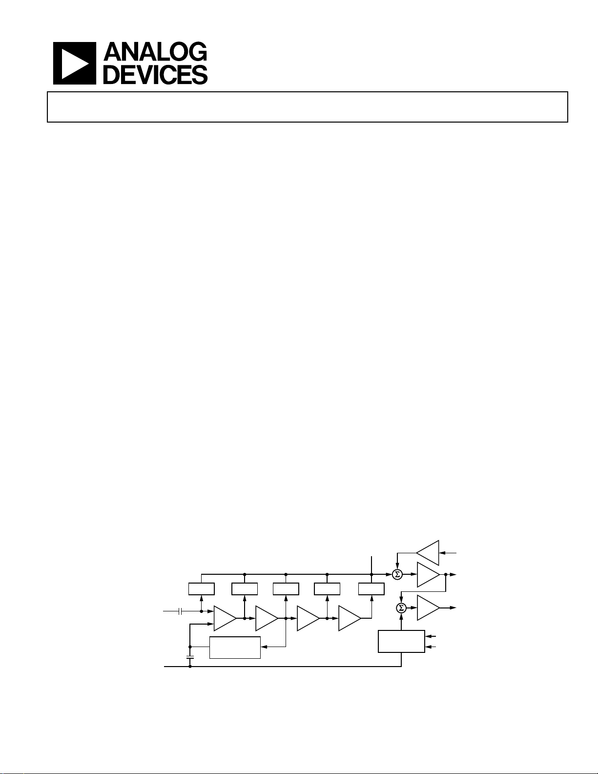
FUNCTIONAL BLOCK DIAGRAM
RF Detector/Controller
AD8314
For convenience, the signal is internally ac-coupled, using a
5 pF capacitor to a load of 3 kΩ in shunt with 2 pF. This highpass coupling, with a corner at approximately 16 MHz,
determines the lowest operating frequency. Therefore, the
source can be dc grounded.
The AD8314 provides two voltage outputs. The first, V_UP,
increases from close to ground to about 1.2 V as the input signal
level increases from 1.25 mV to 224 mV. This output is intended
for use in measurement mode. Consult the
for information on this mode. A capacitor can be connected
between the V_UP and FLTR pins when it is desirable to
increase the time interval over which averaging of the input
waveform occurs.
The second output, V_DN, is an inversion of V_UP but with
twice the slope and offset by a fixed amount. This output starts
at about 2.25 V (provided the supply voltage is ≥3.3 V) for the
minimum input and falls to a value close to ground at the
maximum input. This output is intended for analog control
loop applications. A setpoint voltage is applied to VSET, and
V_DN is then used to control a VGA or power amplifier. Here
again, an external filter capacitor can be added to extend the
averaging time. Consult the
Applications section for
information on this mode.
The AD8314 is available in 8-lead MSOP and 8-lead LFCSP
packages and consumes 4.5 mA from a 2.7 V to 5.5 V supply.
When powered down, the typical sleep current is 20 µA.
Applications section
FLTR
+
10dB
DETDET
BAND GAP
REFERENCE
DETDETDET
RFIN
OFFSET
COMPENSATION
COMM
PADDLE)
Rev. B
Information furnished by Analog Devices is believed to be accurate and reliable. However, no
responsibility is assumed by Anal og Devices for its use, nor for any infringements of patents or ot her
rights of third parties that may result from its use. Specifications subject to change without notice. No
license is granted by implication or otherwise under any patent or patent rights of Analog Devices.
Trademarks and registered trademarks are the property of their respective owners.
10dB10dB 10dB
AD8314
Figure 1.
One Technology Way, P.O. Box 9106, Norwood, MA 02062-9106, U.S.A.
Tel: 781.329.4700 www.analog.com
Fax: 781.461.3113 ©2006 Analog Devices, Inc. All rights reserved.
V-I
–
I-V
–
X2
+
VPOS
ENBL
VSET
V_UP
V_DN
01086-001

AD8314
TABLE OF CONTENTS
Features .............................................................................................. 1
dBV vs. dBm ............................................................................... 13
Applications....................................................................................... 1
General Description......................................................................... 1
Functional Block Diagram .............................................................. 1
Revision History ............................................................................... 2
Specifications..................................................................................... 3
Absolute Maximum Ratings............................................................ 4
ESD Caution.................................................................................. 4
Pin Configurations and Function Descriptions............................ 5
Typical Performance Characteristics ............................................. 6
Theory of Operation ...................................................................... 10
Inverted Output .......................................................................... 11
Applications..................................................................................... 12
Basic Connections...................................................................... 12
Transfer Function in Terms of Slope and Intercept ............... 12
Filter Capacitor ........................................................................... 13
Operating in Controller Mode ................................................. 13
Power-On and Enable Glitch.................................................... 14
Input Coupling Options ............................................................ 14
Increasing the Logarithmic Slope in Measurement Mode ... 15
Effect of Waveform Type on Intercept .................................... 15
Mobile Handset Power Control Examples.............................. 16
Operation at 2.7 GHz................................................................. 18
Using the LFCSP Package.......................................................... 18
Evaluation Board ........................................................................ 18
Outline Dimensions ....................................................................... 20
Ordering Guide .......................................................................... 20
REVISION HISTORY
5/06—Rev. A to Rev. B
Updated Format..................................................................Universal
Changes to General Description .................................................... 1
Changes to Table 1............................................................................ 3
Changes to Table 2............................................................................ 4
Inserted Figure 3; Renumbered Sequentially................................ 5
Changes to Figure 4, Figure 5, Figure 6, Figure 7,
and Figure 8 ...................................................................................... 6
Changes to Figure 9, Figure 10, and Figure 12 ............................. 7
Changes to Figure 37...................................................................... 14
Changes to Table 5.......................................................................... 15
Changes to Figure 39...................................................................... 16
Changes to Table 7.......................................................................... 19
Updated Outline Dimensions....................................................... 20
Changes to Ordering Guide.......................................................... 20
3/02—Rev. 0 to Rev. A
Edit to Product Description.............................................................1
Edit to Specifications.........................................................................2
Edit to Ordering Guide ....................................................................3
Edit to TPC 1......................................................................................4
New Section (Operation at 2.7 GHz) Added.............................. 14
Addition of New Figures 14 and 15 ............................................. 14
Changes to Evaluation Board Section.......................................... 14
Addition of Chip Scale Package.................................................... 16
Rev. B | Page 2 of 20

AD8314
SPECIFICATIONS
VS = 3 V, TA = 25°C, unless otherwise noted.
Table 1.
Parameter Conditions Min Typ Max Unit
OVERALL FUNCTION
Frequency Range
Input Voltage Range Internally ac-coupled 1.25 224 mV rms
Equivalent Power Range 52.3 Ω external termination −45 0 dBm
Logarithmic Slope Main output, V_UP, 100 MHz2 18.85 21.3 23.35 mV/dB
Logarithmic Intercept Main output, V_UP, 100 MHz −68 −62 −56 dBV
Equivalent dBm Level 52.3 Ω external termination −55 −49 −43 dBm
INPUT INTERFACE Pin RFIN
DC Resistance to COMM 100 kΩ
Inband Input Resistance f = 0.1 GHz 3 kΩ
Input Capacitance f = 0.1 GHz 2 pF
MAIN OUTPUT Pin V_UP
Voltage Range V_UP connected to VSET 0.01 1.2 V
Minimum Output Voltage No signal at RFIN, RL ≥ 10 kΩ 0.01 0.02 0.05 V
Maximum Output Voltage3 RL ≥ 10 kΩ 1.9 2 V
General Limit 2.7 V ≤ VS ≤ 5.5 V VS − 1.1 VS − 1 V
Available Output Current Sourcing/sinking 1/0.5 2/1 mA
Response Time 10% to 90%, 10 dB step 70 ns
Residual RF (at 2f) f = 0.1 GHz (worst condition) 100 μV
INVERTED OUTPUT Pin V_DN
Gain Referred to V_UP VDN = 2.25 V − 2 × VUP −2
Minimum Output Voltage VS ≥ 3.3 V 0.01 0.05 0.1 V
Maximum Output Voltage VS ≥ 3.3 V4 2.1 2.2 2.5 V
Available Output Current Sourcing/sinking 4/100 6/200 mA/μA
Output-Referred Noise RF input = 2 GHz, –33 dBV, f
Response Time 10% to 90%, 10 dB input step 70 ns
Full-Scale Settling Time −40 dBm to 0 dBm input step to 95% 150 ns
SETPOINT INPUT Pin VSET
Voltage Range Corresponding to central 40 dB 0.15 1.2 V
Input Resistance 7 10 kΩ
Logarithmic Scale Factor f = 0.900 GHz 20.7 mV/dB
f = 1.900 GHz 19.7 mV/dB
ENABLE INTERFACE Pin ENBL
Logic Level to Enable Power HI condition, −40°C ≤ TA ≤ +85°C 1.6 V
Input Current when HI 2.7 V at ENBL, −40°C ≤ TA ≤ +85°C 20 300 μA
Logic Level to Disable Power LO condition, −40°C ≤ TA ≤ +85°C −0.5 +0.8 V
POWER INTERFACE Pin VPOS
Supply Voltage 2.7 3.0 5.5 V
Quiescent Current 3.0 4.5 5.7 mA
Overtemperature −40°C ≤ TA ≤ +85°C 2.7 4.4 6.6 mA
Total Supply Current when Disabled 20 95 μA
Overtemperature −40°C ≤ TA ≤ +85°C 40 μA
1
For a discussion on operation at higher frequencies, see Applications section.
2
Mean and standard deviation specifications are available in Table 4.
3
Increased output possible when using an attenuator between V_UP and VSET to raise the slope.
4
Refer to Figure 22 for details.
1
To meet all specifications 0.1 2.5 GHz
= 10 kHz 1.05 μV/√Hz
NOISE
V
POS
Rev. B | Page 3 of 20
AD8314
ABSOLUTE MAXIMUM RATINGS
Table 2.
Parameter Value
Supply Voltage VPOS 5.5 V
V_UP, V_DN, VSET, ENBL 0 V, VPOS
Input Voltage 1.6 V rms
Equivalent Power 17 dBm
Internal Power Dissipation 200 mW
θJA (MSOP) 200°C/W
θJA (LFCSP, Paddle Soldered) 80°C/W
θJA (LFCSP, Paddle Not Soldered) 200°C/W
Maximum Junction Temperature 125°C
Operating Temperature Range −40°C to +85°C
Storage Temperature Range −65°C to +150°C
Lead Temperature (Soldering 60 sec)
8-Lead MSOP 300°C
8-Lead LFCSP 240°C
Stresses above those listed under Absolute Maximum Ratings
may cause permanent damage to the device. This is a stress
rating only; functional operation of the device at these or any
other conditions above those indicated in the operational
section of this specification is not implied. Exposure to absolute
maximum rating conditions for extended periods may affect
device reliability.
ESD CAUTION
ESD (electrostatic discharge) sensitive device. Electrostatic charges as high as 4000 V readily accumulate on
the human body and test equipment and can discharge without detection. Although this product features
proprietary ESD protection circuitry, permanent damage may occur on devices subjected to high energy
electrostatic discharges. Therefore, proper ESD precautions are recommended to avoid performance
degradation or loss of functionality.
Rev. B | Page 4 of 20
AD8314
PIN CONFIGURATIONS AND FUNCTION DESCRIPTIONS
RFIN
ENBL
VSET
FLTR
1
AD8314
2
TOP VIEW
3
(Not to Scale)
4
8
7
6
5
VPOS
V_DN
V_UP
COMM
01086-002
Figure 2. RM-8 Pin Configuration
1RFIN
2ENBL
AD8314
TOP VIEW
3VSET
(Not to Scale)
4FLTR
Figure 3. CP-8-1 Pin Configuration
8VPOS
7V_DN
5V_UP
5COMM
01086-003
Table 3. Pin Function Descriptions
Pin No. Mnemonic Description
1 RFIN RF Input.
2 ENBL Connect Pin to VS for Normal Operation. Connect pin to ground for disable mode.
3 VSET Setpoint Input for Operation in Controller Mode. To operate in detector mode connect VSET to V_UP.
4 FLTR
Connection for an External Capacitor to Slow the Response of the Output. Capacitor is connected between
FLTR and V_UP.
5 COMM Device Common (Ground)
6 V_UP Logarithmic Output. Output voltage increases with increasing input amplitude.
7 V_DN Inversion of V_UP, Governed by: V_DN = 2.25 V − 2 × VUP.
8 VPOS Positive Supply Voltage (VS), 2.7 V to 5.5 V.
Rev. B | Page 5 of 20
AD8314
TYPICAL PERFORMANCE CHARACTERISTICS
1.2
1.0
0.8
(V)
0.6
UP
V
0.4
0.2
0.1GHz
0.9GHz
1.9GHz
2.5GHz
4
3
2
1
0
ERROR (dB)
–1
–2
–3
1.9GHz
2.5GHz
0.1GHz
0.9GHz
0
–75 –5
–65 –55 –45 –35 – 25 –15
INPUT AMPLI TUDE (dBV)(–52dBm) (–2dBm)
Figure 4. V
vs. Input Amplitude
UP
1.2
1.0
+25°C
0.8
–40°C
(V)
0.6
UP
V
0.4
0.2
0
–70 0
–60 – 50 –40 –30 –20 –10
Figure 5. V
UP
+85°C
+25°C
SLOPE AND INTERCEPT
NORMALIZE D AT +25°C AND
APPLIED T O –40°C AND +85°C
INPUT AMPLI TUDE (dBV)(–47dBm) (+3dBm)
and Log Conformance vs. Input Amplitude at 0.1 GHz;
−40°C, +25°C, and +85°C
1.2
1.0
0.8
(V)
0.6
UP
–40°C
V
0.4
+25°C
+85°C
–40°C
–4
01086-004
–60 –50 –40 –30 –20 –10
–70 0
INPUT AMPLITUDE (dBV)(–47dBm) (+ 3dBm)
01086-007
Figure 7. Log Conformance vs. Input Amplitude
3
2
1
0
ERROR (dB)
–1
–2
–3
01086-005
1.2
1.0
0.8
(V)
0.6
UP
V
0.4
0.2
0
–70 0
Figure 8. V
+85°C
+25°C
–40°C
SLOPE AND INTERCEPT
NORMALIZED AT +25°C AND
APPLIED T O –40°C AND +85° C
–60 –50 –40 –30 – 20 –10
INPUT AMPLI TUDE (dBV)(–47dBm) (+3dBm)
and Log Conformance vs. Input Amplitude at 1.9 GHz;
UP
3
2
1
0
ERROR (dB)
–1
–2
–3
01086-008
−40°C, +25°C, and +85°C
3
2
1
0
ERROR (dB)
–1
1.2
1.0
0.8
(V)
0.6
UP
V
0.4
+85°C
+25°C
–40°C
+85°C
3
2
1
0
ERROR (dB)
–1
0.2
0
–70 0
–60 – 50 –40 –30 –20 –10
Figure 6. V
UP
SLOPE AND INTERCEPT
NORMALIZED AT +25°C AND
APPLI ED TO –40°C AND +85° C
INPUT AMPLI TUDE (dBV)(–47dBm) (+3dBm)
and Log Conformance vs. Input Amplitude at 0.9 GHz;
−40°C, +25°C, and +85°C
–2
–3
01086-006
Rev. B | Page 6 of 20
0.2
0
–70 0
Figure 9. V
SLOPE AND INT ERCEPT
NORMALIZED AT +25°C AND
APPLIED T O –40°C AND +85° C
–60 – 50 –40 –30 –20 –10
INPUT AMPLI TUDE (dBV)(–47dBm) (+3dBm)
and Log Conformance vs. Input Amplitude at 2.5 GHz;
UP
−40°C, +25°C, and +85°C
–2
–3
01086-009

AD8314
–
–
23
22
21
+25°C
20
SLOPE (mV/dB)
UP
V
19
18
02
–40°C
+85°C
0.5 1.0 1.5 2.0
FREQUENCY (G Hz)
.5
01086-010
Figure 10. Slope vs. Frequency; −40°C, +25°C, and +85°C
22
0.1GHz
21
0.9GHz
SLOPE (mV/dB)
UP
20
V
1.9GHz
55
–60
–65
INTERCEPT (dBV)
UP
V
–70
–75
02.5
Figure 13. V
0.5 1.0 1.5 2.0
Intercept vs. Frequency; −40°C, +25°C, and +85°C
UP
+85°C
FREQUENCY (GHz)
–40°C
+25°C
01086-013
61
–62
–63
–64
INTERCEPT (dBV)
–65
UP
V
0.1GHz
2.5GHz
0.9GHz
2.5GHz
19
3.0 3.5 4. 0 4.5 5. 0
2.5 5.5
V
(V)
S
Figure 11. V
Slope vs. Supply Voltage
UP
01086-011
–66
–67
2.5 5.5
3500
3000
2500
2000
1500
RESISTANCE ( Ω)
1000
500
0
02
X
FREQUENCY (GHz)
0.1
0.9
1.9
2.5
R
0.5 1.0 1.5 2.0
FREQUENCY (GHz)
R ||
3030 ||
760 ||
301 ||
90 ||
X
R
- jXΩ
- j748Ω
- j106Ω
- j80Ω
- j141Ω
Figure 12. Input Impedance
0
–200
–400
–600
–800
REACTANCE (Ω)
–1000
–1200
–1400
.5
01086-012
6
5
4
DECREASING
3
2
1
SUPPLY CURRENT (mA)
0
–1
0.2 2.6
0.4 0.6 0.8 1.0 1.2 1.4 1.6 1.8 2.0 2.2 2.4
Figure 15. Supply Current vs. ENBL Voltage, V
1.9GHz
3.0 3.5 4. 0 4.5 5. 0
V
(V)
S
Figure 14. V
Intercept vs. Supply Voltage
UP
V
ENBL
V
ENBL
(V)
INCREASING
V
ENBL
= 3 V
S
01086-014
01086-015
Rev. B | Page 7 of 20

AD8314
V
–
V
AVERAGE: 128 SAMPLES
VDN500mV/VERTI CAL
DIVIS ION
GND
V
DN
V
500mV/VERTI CAL DIVISION
UP
GND
V
ENBL
UP
GND
5V PER VERTICAL DIVISION
V
ENBL
Figure 16. ENBL Response Time
VPOS
V_DN
V_UP
COMM
EXT TRIG
8
7
6
5
PULSE OUT
TEK P6204
FET PROBE
TEK P6204
FET PROBE
HP8648B
SIGNAL
GENERATOR
33dB
52.3Ω
10MHz REF OUT PUT
RF OUT
NC
1
RFIN
ENBL
2
AD8314
3
VSET
FLTR
4
NC = NO CONNECT
Figure 17. Test Setup for ENBL Response Time
80
75
70
65
60
55
50
45
40
35
30
25
AMPLITUDE (d B)
20
15
10
5
0
–5
100 1k 10k 100k 1M
10 10M
FREQUENCY (Hz)
Figure 18. AC Response from VSET to V_DN
1µs PER
HORIZONT AL
DIVISION
HP8116A
PULSE
GENERATOR
3.0V
0.1µF
TRIG
OUT
TRIG
TEK
TDS784C
SCOPE
0
–10
–20
–30
–40
–50
–60
–70
–80
–90
–100
–110
–120
–130
–140
–150
–160
–170
V
500mV/
UP
VERTICAL
DIVISION
GND
RF INPUT
GND
200mV PER
VERTICAL
DIVISION
01086-016
Figure 19. V
HP8648B
SIGNAL
GENERATOR
PULSE
MODULATI ON
MODE
RF OUT
RF
SPLITTER
–3dB
52.3Ω
3.0V
and VDN Response Time, −40 dBm to 0 dBm
UP
10MHz REF OUTPUT
PULSE MODE IN
–3dB
1
2
FET PROBE
RFIN
ENBL
TEK P6204
AD8314
3
VSET
FLTR
4
NC
01086-017
NC
NC = NO CONNECT
COMM
Figure 20. Text Setup for Pulse Response
10
40dBm–
1
PHASE (Degrees )
NOISE SPECTRAL DENSITY (µV/√Hz)
0.1
100 10M
01086-018
–20dBm
1k 10k 100k 1M
FREQUENCY (Hz)
Figure 21. V
DN
AVERAGE: 128 S AMPLES
VDN1V/VERTI CAL
DIVISION
PULSED RF
0.1GHz, –13d BV
100ns PER
HORIZONT AL
DIVISION
VPOS
V_DN
V_UP
EXT TRIG
8
7
6
5
OUT
TEK P6204
FET PROBE
TEK P6204
FET PROBE
PICOSECOND
PULSE LABS
GENERATOR
0.1µF
–50dBm
–30dBm
–60dBm
Noise Spectral Density
PULSE
3.0V
RF INPUT
–70dBm
01086-019
TRIG
OUT
TEK
TDS784C
SCOPE
TRIG
01086-021
01086-020
Rev. B | Page 8 of 20

AD8314
–
V
2.3
2.2
2.1
0mA
2mA
4mA
2.3
2.2
2.1
SHADING INDICAT ES
±3 SIGMA
(V)
2.0
DN
V
1.9
1.8
1.7
2.8 2.9 3.0 3.1 3.2 3.3 3.4
2.7 3.5
Figure 22. Maximum V
6mA
(V)
V
S
Voltage vs. VS by Load Current
DN
AVERAGE: 128 SAMPLES
V
500mV/VERTI CAL
UP
DIVISION
500mV/VERTI CAL
V
UP
DIVISION
1µs PER
HORIZONT AL
DIVISIO N
2V PER
VERTICAL
DIVIS ION
V
GND
DN
VUP GND
GND
V
UP
VPOS AND ENABLE
Figure 23. Power-On and Power-Off Response, Measurement Mode
HP8648B
SIGNAL
GENERATOR
33dB
10MHz REF OUT PUT
RF OUT
EXT TRIG
HP8116A
GENERATOR
AD811
PULSE
PULSE
OUT
49.9Ω
TRIG
OUT
(V)
2.0
DN
V
1.9
1.8
1.7
2.8 2.9 3.0 3.1 3.2 3.3 3. 4
2.7 3.5
V
01086-022
Figure 25. Maximum V
(V)
S
Voltage vs. VS with 3 mA Load
DN
01086-025
AVERAGE: 128 SAMPLES
200mV PER
VERTICAL
DIVISIO N
V
DN
GND
V
DN
VPOS AND ENABLE
2V PER
VERTICAL
GND
01086-023
Figure 26. Power-On Response, V
DIVISIO N
, Controller Mode with VSET Held Low
DN
100ns PER
HORIZONT AL
DIVISION
01086-026
PULSE
OUT
49.9Ω
TRIG
OUT
HP8648B
SIGNAL
GENERATOR
RF OUT
10MHz REF OUTPUT
EXT TRIG
GENERATOR
AD811
HP8112A
PULSE
732Ω
8
AD8314
VPOS
V_DN
V_UP
COMM
7
6
5
TEK P6204
FET PROBE
TEK P6204
FET PROBE
52.3Ω
RFIN
1
ENBL
2
3
VSET
FLTR
4
NC
NC = NO CONNECT
Figure 24. Test Setup for Power-On and Power-Off Response
TRIG
TEK
TDS784C
SCOPE
VPOS
V_DN
52.3Ω
1
2
RFIN
ENBL
AD8314
3
0.2
01086-024
VSET
FLTR
4
NC
NC = NO CONNECT
V_UP
COMM
Figure 27. Test Setup for Power-On Response at V_DN Output,
Controller Mode with VSET Pin Held Low
8
7
6
5
NC
732Ω
TEK P6204
FET PROBE
TRIG
TEK
TDS784C
SCOPE
01086-027
Rev. B | Page 9 of 20

AD8314
(
THEORY OF OPERATION
The AD8314 is a logarithmic amplifier (log amp) similar in
design to the AD8313; further details about the structure and
function can be found in the
amps produced by ADI.
AD8313 data sheet and other log
Figure 28 shows the main features of
the AD8314 in block schematic form.
The AD8314 combines two key functions needed for the
measurement of signal level over a moderately wide dynamic
range. First, it provides the amplification needed to respond to
small signals, in a chain of four amplifier/limiter cells, each
having a small signal gain of 10 dB and a bandwidth of
approximately 3.5 GHz. At the output of each of these amplifier
stages is a full-wave rectifier, essentially a square-law detector
cell, that converts the RF signal voltages to a fluctuating current
having an average value that increases with signal level. A
further passive detector stage is added prior to the first stage.
Therefore, there are five detectors, each separated by 10 dB,
spanning some 50 dB of dynamic range. The overall accuracy at
the extremes of this total range, viewed as the deviation from an
ideal logarithmic response, that is, the law-conformance error,
can be judged by reference to
across the central 40 dB are moderate.
through
Figure 11, Figure 13, and Figure 14 show how the
Figure 7, which shows that errors
Figure 5, Figure 6, Figure 8
conformance to an ideal logarithmic function varies with
supply voltage, temperature, and frequency.
The output of these detector cells is in the form of a differential
current, making their summation a simple matter. It can easily
be shown that such summation closely approximates a logarithmic
function. This result is then converted to a voltage, at Pin V_UP,
through a high-gain stage. In measurement modes, this output
is connected back to a voltage-to-current (V-I) stage, in such a
manner that V_UP is a logarithmic measure of the RF input
voltage, with a slope and intercept controlled by the design. For
a fixed termination resistance at the input of the AD8314, a
given voltage corresponds to a certain power level.
However, in using this part, it must be understood that log
amps do not fundamentally respond to power. It is for this
reason the dBV is used (decibels above 1 V rms) rather than the
commonly used metric of dBm. While the dBV scaling is fixed,
independent of termination impedance, the corresponding
power level is not. For example, 224 mV rms is always −13 dBV
(with one further condition of an assumed sinusoidal waveform;
see the
Applications section for more information on the effect
of waveform on logarithmic intercept), and it corresponds to a
power of 0 dBm when the net impedance at the input is 50 Ω.
When this impedance is altered to 200 Ω, the same voltage
clearly represents a power level that is four times smaller
2
(P = V
/R), that is, −6 dBm. Note that dBV can be converted to
dBm for the special case of a 50 Ω system by simply adding
13 dB (0 dBV is equivalent to +13 dBm).
Therefore, the external termination added prior to the AD8314
determines the effective power scaling. This often takes the
form of a simple resistor (52.3 Ω provides a net 50 Ω input),
but more elaborate matching networks can be used. This
impedance determines the logarithmic intercept, the input
power for which the output would cross the baseline (V_UP =
zero) if the function were continuous for all values of input.
Because this is never the case for a practical log amp, the
intercept refers to the value obtained by the minimum-error
straight-line fit to the actual graph of V_UP vs. PIN (more
generally, V
). Again, keep in mind that the quoted values
IN
assume a sinusoidal (CW) signal. Where there is complex
modulation, as in CDMA, the calibration of the power response
needs to be adjusted accordingly. Where a true power (waveformindependent) response is needed, the use of an rms-responding
detector, such as the
AD8361, should be considered.
RFIN
COMM
PADDLE)
OFFSET
COMPENSATION
DETDETDET
10dB10dB 10dB
Figure 28. Block Schematic
10dB
AD8314
FLTR
DETDET
+
BAND GAP
REFERENCE
V-I
–
I-V
–
X2
+
VPOS
ENBL
VSET
V_UP
V_DN
01086-028
Rev. B | Page 10 of 20

AD8314
Table 4. Typical Specifications at Selected Frequencies at 25°C (Mean and Σ)
±1 dB Dynamic Range1 (dBV)
Slope (mV/dB) Intercept (dBV)
Frequency (GHz)
μ σ μ σ μ σ μ σ
0.1 21.3 0.4 −62.2 0.4 –11.8 0.3 −59 0.5
0.9 20.7 0.4 −63.6 0.4 –13.8 0.3 −61.4 0.4
1.9 19.7 0.4 −66.3 0.4 –19 0.7 −64 0.6
2.5 19.2 0.4 −62.1 0.7 –16.4 1.7 −61 1.3
1
Refer to Figure 32.
However, the logarithmic slope, the amount by which the
output V_UP changes for each decibel of input change (voltage
or power) is, in principle, independent of waveform or termination
CURRENTS F ROM
DETECTORS
impedance. In practice, it usually falls off somewhat at higher
frequencies, due to the declining gain of the amplifier stages
AD8314
and other effects in the detector cells. For the AD8314, the slope
at low frequencies is nominally 21.3 mV/dB, falling almost
linearly with frequency to about 19.2 mV/dB at 2.5 GHz. These
values are sensibly independent of temperature (see
and almost totally unaffected by the supply voltage from 2.7 V
to 5.5 V (see
Figure 11).
Figure 10)
2.5
2.0
INVERTED OUTPUT
The second provision is the inclusion of an inverting amplifier
to the output, for use in controller applications. Most power
amplifiers require a gain-control bias that must decrease from a
large positive value toward ground level as the power output is
required to decrease. This control voltage, which appears at
Pin V_DN, is not only of the opposite polarity to V_UP, but also
needs to have an offset added to determine its most positive value
when the power level (assumed to be monitored through a
directional coupler at the output of the PA) is minimal.
The starting value of V_DN is nominally 2.25 V, and it falls on a
slope of twice that of V_UP; in other words,−43 mV/dB.
Figure 29
shows how this is achieved: the reference voltage that determines
the maximum output is derived from the on-chip voltage
reference and is substantially independent of the supply voltage
or temperature. However, the full output cannot be attained for
supply voltages under 3.3 V;
The relationship between V_UP and V_DN is shown in
Figure 22 shows this dependency.
Figure 30.
1.5
VOLTS
1.0
0.5
High Point Low Point
I-V
FLTR
BAND GAP
REFERENCE
V-I
+
VSET
Figure 29. Output Interfaces
OUTPUT FOR
PA CONTROL
V_DN
OUTPUT FOR
MEASUREMENT
0
–50 –40 –30 –20 –10
–60 0
V_UP
INPUT AMPLITUDE (dBV)
Figure 30. Showing V_UP and V_DN Relationship
+2
V
= 2.25V – 2.0 × V_UP
DN
1.125V
V_UP
V_DN
01086-030
01086-029
Rev. B | Page 11 of 20

AD8314
F
APPLICATIONS
BASIC CONNECTIONS
Figure 31 shows connections for the basic measurement mode.
A supply voltage of 2.7 V to 5.5 V is required. The supply to the
VPOS pin should be decoupled with a low inductance 0.1 µF
surface-mount ceramic capacitor. A series resistor of about 10 Ω
can be added; this resistor slightly reduces the supply voltage to the
AD8314 (maximum current into the VPOS pin is approximately
9 mA when V_DN is delivering 5 mA). Its use should be
avoided in applications where the power supply voltage is very
low (that is, 2.7 V). A series inductor provides similar power
supply filtering with minimal drop in supply voltage.
52.3Ω
INPUT
1
RFIN
V
S
ENBL
2
VPOS
V_DN
AD8314
V_UP
COMM
C
F
OPTIONAL
(SEE TEXT)
3
4
VSET
FLTR
Figure 31. Basic Connections for Operation in Measurement Mode
The ENBL pin is here connected to VPOS. The AD8314 can be
disabled by pulling this pin to ground when the chip current is
reduced to about 20 µA from its normal value of 4.5 mA. The
logic threshold is around +V
/2 and the enable function occurs
S
in about 1.5 µs. Note, however, further settling time is generally
needed at low input levels.
The AD8314 has an internal input coupling capacitor. This
eliminates the need for external ac coupling. A broadband input
match is achieved in this example by connecting a 52.3 Ω resistor
between RFIN and ground. This resistance combines with the
internal input impedance of approximately 3 kΩ to give an
overall broadband input resistance of 50 Ω. Several other
coupling methods are possible, which are described in the
Input Coupling Options section.
The measurement mode is selected by connecting VSET to
V_UP, which establishes a feedback path and sets the
logarithmic slope to its nominal value. The peak voltage range
of the measurement extends from −58 dBV to −13 dBV at
0.9 GHz, and only slightly less at higher frequencies up to
2.5 GHz. Therefore, using the 50 Ω termination, the equivalent
power range is −45 dBm to 0 dBm. At a slope of 21.5 mV/dB,
this would amount to an output span of 967 mV.
shows the transfer function for V_UP at a supply voltage of 3 V
and input frequency of 0.9 GHz.
0.1µ
8
OPTIONAL
(SEE TEXT)
7
6
5
V
V
V
Figure 32
S
DN
UP
01086-031
V_DN, which is generally not used when the AD8314 is used in
measurement mode, is essentially an inverted version of V_UP.
The voltage on V_UP and V_DN are related by
= 2.25 V − 2 V
V
DN
UP
While V_DN can deliver up to 6 mA, the load resistance on
V_UP should not be lower than 10 kΩ in order that the fullscale output of 1 V can be generated with the limited available
current of 200 µA maximum.
Figure 32 shows the logarithmic
conformance under the same conditions.
1.2
1.0
0.8
(V)
0.6
UP
V
0.4
0.2
VS = 3V
R
= 52.3Ω
T
±1dB DYNAMIC RANGE
±3dB DYNAMIC RANGE
0
–70 0
(–47dBm) (+3dBm)
INTERCEPT
–60 –50 –40 –30 –20 –10
INPUT AMPLITUDE (dBV)
Figure 32. V
and Log Conformance Error vs.
UP
Input Level vs. Input Level at 900 MHz
3
2
1
0
ERROR (d B)
–1
–2
–3
TRANSFER FUNCTION IN TERMS OF SLOPE AND
INTERCEPT
The transfer function of the AD8314 is characterized in terms
of its slope and intercept. The logarithmic slope is defined as the
change in the RSSI output voltage for a 1 dB change at the input.
For the AD8314, slope is nominally 21.5 mV/dB. Therefore, a
10 dB change at the input results in a change at the output of
approximately 215 mV. Log conformance plot,
the range over which the device maintains its constant slope.
The dynamic range can be defined as the range over which the
error remains within a certain band, usually ±1 dB or ±3 dB. In
Figure 32 for example, the ±1 dB dynamic range is approximately
50 dB (from −13 dBV to −63 dBV).
Figure 32, shows
01086-032
Rev. B | Page 12 of 20

AD8314
F
The intercept is the point at which the extrapolated linear
response would intersect the horizontal axis (see
Figure 32).
Using the slope and intercept, the output voltage can be
calculated for any input level within the specified input range by
= V
V
UP
× (PIN − PO)
SLOPE
where:
V
is the demodulated and filtered RSSI output.
UP
V
is the logarithmic slope, expressed in V/dB.
SLOPE
PIN is the input signal, expressed in decibels relative to some
reference level (either dBm or dBV in this case).
P
is the logarithmic intercept, expressed in decibels relative to
O
the same reference level.
For example, at an input level of −40 dBV (−27 dBm), the
output voltage is
V
= 0.020 V/dB × [−40 dBV − (−63 dBV)] = 0.46 V
OUT
dBV VS. dBm
The most widely used convention in RF systems is to specify
power in dBm, that is, decibels above 1 mW in 50 Ω. Specification
of log amp input levels in terms of power is strictly a concession
to popular convention; they do not respond to power (tacitly
power absorbed at the input), but to the input voltage. The use
of dBV, defined as decibels with respect to a 1 V rms sine wave,
is more precise, although this is still not unambiguous because
waveform is also involved in the response of a log amp, which,
for a complex input (such as a CDMA signal), does not follow
the rms value exactly. Since most users specify RF signals in
terms of power (more specifically, in dBm/50 Ω), both dBV and
dBm are used in specifying the performance of the AD8314
showing equivalent dBm levels for the special case of a
50 Ω environment. Values in dBV are converted to
dBm re 50 Ω by adding 13.
FILTER CAPACITOR
The video bandwidth of both V_UP and V_DN is
approximately 3.5 MHz. In CW applications where the input
frequency is much higher than this, no further filtering of the
demodulated signal is required. Where there is a low frequency
modulation of the carrier amplitude, however, the low-pass
corner must be reduced by the addition of an external filter
capacitor, C
to C
F
(see Figure 31). The video bandwidth is related
F
by
BandwidthVideo
=
1
()
pF5.3k13π2
C
+××
F
OPERATING IN CONTROLLER MODE
Figure 33 shows the basic connections for operation in the
controller mode, and
typical controller mode application. The feedback from V_UP
to VSET is broken and the desired setpoint voltage is applied to
VSET from the controlling source (often this is a DAC). V
rails high (2.2 V on a 3.3 V supply, and 1.9 V on a 2.7 V supply)
when the applied power is less than the value corresponding to
the setpoint voltage. When the input power slightly exceeds this
value, V
would, in the absence of the loop via the power
DN
amplifier gain pin, decrease rapidly toward ground. In the
closed loop, however, the reduction in V
amplifier to reduce its output. This restores a balance between
the actual power level sensed at the input of the AD8314 and
the demanded value determined by the setpoint. This assumes
that the gain control sense of the variable gain element is
positive, that is, an increasing voltage from V_DN tends to
increase gain. The output swing and current sourcing capability
of V_DN are shown in
INPUT
VSET
Figure 33. Basic Connections for Operation in Controller Mode
DIRECTIONAL
COUPLER
Figure 34. Typical Controller Mode Application
The relationship between the input level and the setpoint
voltage follows from the nominal transfer function of the device
vs. input amplitude, see Figure 4). For example, a voltage of
(V
UP
1 V on VSET demands a power level of 0 dBm at RFIN. The
corresponding power level at the output of the power amplifier
is greater than this amount due to the attenuation through the
directional coupler.
Figure 34 shows a block diagram of a
DN
Figure 22 and Figure 25.
52.3Ω
8
AD8314
C
F
AMPLIFIER
C
F
FLTR
RFIN
VPOS
V_DN
V_UP
COMM
POWER
V_UP
AD8314
7
6
5
V_DN
RFIN
1
V
S
ENBL
2
3
VSET
FLTR
4
52.3Ω
DN
causes the power
0.1µ
V
S
V
DN
RF INPUT
GAIN
CONTROL
VOLTAGE
VSET
DAC
01086-033
01086-034
Rev. B | Page 13 of 20

AD8314
When connected in a PA control loop, as shown in Figure 34,
the voltage V
setting up the required averaging time, by choice of C
is not explicitly used but is implicated in again
UP
.
F
However, now the effective loop response time is a much more
complicated function of the PA’s gain-control characteristics,
which are very nonlinear. A complete solution requires specific
knowledge of the power amplifier.
The transient response of this control loop is determined by the
filter capacitor, C
When this is large, the loop is unconditionally
F.
stable (by virtue of the dominant pole generated by this
capacitor), but the response is sluggish. The minimum value
ensuring stability should be used, requiring full attention to the
particulars of the power amplifier control function. Because this
is invariably nonlinear, the choice must be made for the worstcase condition, which usually corresponds to the smallest
output from the PA, where the gain function is steepest. In
practice, an improvement in loop dynamics can often be
achieved by adding a response zero, formed by a resistor in
series with C
.
F
A reactive match can also be implemented as shown in
This is not recommended at low frequencies as device
tolerances dramatically varies the quality of the match because
of the large input resistance. For low frequencies,
Figure 37 is recommended.
In
Figure 36, the matching components are drawn as general
reactances. Depending on the frequency, the input impedance at
that frequency, and the availability of standard value components,
either a capacitor or an inductor is used. As in the previous
case, the input impedance at a particular frequency is plotted on
a Smith Chart and matching components are chosen (shunt or
Series L, shunt or Series C) to move the impedance to the center
of the chart.
Tabl e 5 gives standard component values for some
popular frequencies. Matching components for other frequencies
can be calculated using the input resistance and reactance data
over frequency, which is given in
Figure 12. Note that the
reactance is plotted as though it appears in parallel with the
input impedance (which it does because the reactance is
primarily due to input capacitance).
Figure 36.
Figure 35 or
POWER-ON AND ENABLE GLITCH
As previously mentioned, the AD8314 can be put into a low
power mode by pulling the ENBL pin to ground. This reduces
the quiescent current from 4.5 mA to 20 µA. Alternatively, the
supply can be turned off to eliminate the quiescent current.
Figure 16 and Figure 26 show the behavior of the V_DN output
under these two conditions (in
Figure 26, ENBL is tied to
VPOS). The glitch that results in both cases can be reduced by
loading the V_DN output.
INPUT COUPLING OPTIONS
The internal 5 pF coupling capacitor of the AD8314, along with
the low frequency input impedance of 3 kΩ, gives a high-pass
input corner frequency of approximately 16 MHz. This sets the
minimum operating frequency.
show three options for input coupling. A broadband resistive
match can be implemented by connecting a shunt resistor to
ground at RFIN (see
Figure 35). This 52.3 Ω resistor (other
values can also be used to select different overall input
impedances) combines with the input impedance of the
AD8314 (3 kΩ||2 pF) to give a broadband input impedance of
50 Ω. While the input resistance and capacitance (CIN and
RIN) varies by approximately ±20% from device to device, the
dominance of the external shunt resistor means that the variation
in the overall input impedance is close to the tolerance of the
external resistor.
At frequencies above 2 GHz, the input impedance drops below
250 Ω (see
Figure 12), so it is appropriate to use a larger value
shunt resistor. This value is calculated by plotting the input
impedance (resistance and capacitance) on a Smith Chart and
choosing the best value shunt resistor to bring the input
impedance closest to the center of the chart. At 2.5 GHz, a
shunt resistor of 165 Ω is recommended.
Figure 35 through Figure 37
The impedance matching characteristics of a reactive matching
network provide voltage gain ahead of the AD8314; this increases
the device sensitivity (see
GainVoltage
Tabl e 5). The voltage gain is calculated by
2
R
=
log20
dB
10
1
R
where R2 is the input impedance of the AD8314, and R1 is the
source impedance to which the AD8314 is being matched. Note
that this gain is only achieved for a perfect match. Component
tolerances and the use of standard values tend to reduce gain.
50Ω SOURCE
50Ω SOURCE
50Ω
STRIPLINE
50Ω
R
SHUNT
52.3Ω
Figure 35. Broadband Resistive
X1
Figure 36. Narrowband Reactive
RFIN
50Ω
R
ATTN
Figure 37. Series Attenuation
X2
C
RFIN
RFIN
AD8314
C
V
C
C
CINR
BIAS
AD8314
C
INRIN
V
BIAS
AD8314
C
C
C
V
BIAS
IN
INRIN
01086-037
01086-035
01086-036
Rev. B | Page 14 of 20

AD8314
Figure 37 shows a third method for coupling the input signal
into the AD8314, applicable in applications where the input
signal is larger than the input range of the log amp. A series
resistor, connected to the RF source, combines with the input
impedance of the AD8314 to resistively divide the input signal
being applied to the input. This has the advantage of very little
power being tapped off in RF power transmission applications.
Table 5. X1 and X2 Recommended Components in Figure 36
Frequency (GHz) X1 X2 Voltage Gain (dB)
0.1 Short 52.3 Ω
0.9 33 nH 39 nH 11.8
1.9 10 nH 15 nH 7.8
2.5 1.5 pF 3.9 nH 2.55
INCREASING THE LOGARITHMIC SLOPE IN
MEASUREMENT MODE
The nominal logarithmic slope of 21.5 mV/dB (see Figure 10
for the variation of slope with frequency) can be increased to an
arbitrarily high value by attenuating the signal between V_UP
and VSET, as shown in
⎛
⎜
=
RR
⎜
⎝
In the example shown, two 5 kΩ resistors combine to change
the slope at 1900 MHz from 20 mV/dB to 40 mV/dB. The slope
can be increased to higher levels. This, however, reduces the
usable dynamic range of the device.
AD8314
Figure 38. The ratio R1/R2 is set by
⎞
SlopeNew
⎟
12/1 −
⎟
SlopeOriginal
⎠
V_UP
VSET
Figure 38. Increasing the Output Slope
R1
5kΩ
R2
5kΩ
40mV/dB
@ 1900MHz
01086-038
EFFECT OF WAVEFORM TYPE ON INTERCEPT
Although specified for input levels in dBm (dB relative to
1 mW), the AD8314 fundamentally responds to voltage and not
to power. A direct consequence of this characteristic is that
input signals of equal rms power but differing crest factors
produces different results at the log amp’s output.
The effect of differing signal waveforms is to shift the effective
value of the intercept upwards or downwards. Graphically, this
looks like a vertical shift in the log amp’s transfer function. The
logarithmic slope, however, is not affected. For example,
consider the case of the AD8314 being alternately fed by an
unmodulated sine wave and by a single CDMA channel of the
same rms power. The AD8314’s output voltage differs by the
equivalent of 3.55 dB (70 mV) over the complete dynamic range
of the device (the output for a CDMA input being lower).
Tabl e 6 shows the correction factors that should be applied to
measure the rms signal strength of various signal types. A sine
wave input is used as a reference. To measure the rms power of
a square wave, for example, the mV equivalent of the dB value
given in the table (20 mV/dB times 3.01 dB) should be
subtracted from the output voltage of the AD8314.
Table 6. Shift in AD8314 Output for Signals with Differing
Crest Factors
Correction
Factor (Add
to Measured
Signal Type
Sine Wave 0 dB
Square Wave −3.01 dB
GSM Channel (All Time Slots On) +0.55 dB
CDMA Channel (Forward Link, 9 Channels On) +3.55 dB
CDMA Channel (Reverse Link) +0.5 dB
PDC Channel (All Time Slots On) +0.58 dB
Input Level)
Rev. B | Page 15 of 20

AD8314
MOBILE HANDSET POWER CONTROL EXAMPLES
Figure 39 shows a complete power amplifier control circuit for a
dual mode handset. This circuit is applicable to any dual mode
handset using TDMA or CDMA technologies. The PF08107B
(Hitachi) is driven by a nominal power level of 3 dBm. Some of
the output power from the PA is coupled off using an
LDC15D190A0007A (Murata) directional coupler. This has a
coupling factor of approximately 19 dB for its lower frequency
band (897.5 MHz ± 17.5 MHz) and 14 dB for its upper band
(1747.5 MHz ± 37.5 MHz) and an insertion loss of 0.38 dB
and 0.45 dB, respectively. Because the PF08107B transmits a
maximum power level of 35 dBm, additional attenuation of
15 dB is required before the coupled signal is applied to
the AD8314.
3.5V
4.7µF
1000pF
BAND
SELECT
0V/2V
POUT BAND 1
RFIN
ENBL
VSET
FLTR
35dBm MAX
49.9Ω
POUT BAND 2
32dBm MAX
AD8314
VPOS
V_DN
V_UP
COMM
V
PF08107B
(HITACHI)
V
0.1µF
8
7
6
5
CTL
APC
V
2.7V
S
PIN BAND 1
3dBm
PIN BAND 2
3dBm
TO
ANTENNA
ATTN
15dB
VSET
0V TO 1.1V
LDC15D190A0007A
7
1
8
4
5
3
26
52.3Ω
0dBm
MAX
1
V
S
2
3
4
The setpoint voltage, in the 0 V to 1.1 V range, is applied to the
VSET pin of the AD8314. This is typically supplied by a DAC.
This voltage is compared to the input level of the AD8314. Any
imbalance between VSET and the RF input level is corrected by
V_DN, which drives the V
(gain control) of the power
APC
amplifier. V_DN reaches a maximum value of approximately
1.9 V on a 2.7 V supply (this is higher for higher supply
voltages) while delivering approximately 3 mA to the V
A filter capacitor (C
choice of C
depends to a large degree on the gain control
F
) must be used to stabilize the loop. The
F
input.
APC
dynamics of the power amplifier, something that is frequently
characterized poorly, so some trial and error can be necessary.
In this example, a 220 pF capacitor gives the loop sufficient
speed to follow the GSM and DCS1800 time slot ramping
profiles, while still having a stable, critically damped response.
C
F
220pF
1086-039
Figure 39. A Dual Mode Power Amplifier Control Circuit
Rev. B | Page 16 of 20

AD8314
V
V
Figure 40 shows the relationship between the setpoint voltage,
V
and output power at 0.9 GHz. The overall gain control
SET
function is linear in dB for a dynamic range of over 40 dB.
Figure 41 shows a similar circuit for a single band handset
power amplifier. The BGY241 (Phillips) is driven by a nominal
power level of 0 dBm. A 20 dB directional coupler, DC09-73
(Alpha), is used to couple the signal in this case.
Figure 42
shows the relationship between the control voltage and the
output power at 0.9 GHz.
In both of these examples, noise on the V_DN pin can be reduced
by placing a simple RC low-pass filter between V
and the gain
DN
control pin of the power amplifier. However, the value of the
resistor should be kept low to minimize the voltage drop across
it due to the dc current flowing into the gain control input.
40
30
20
10
0
POUT (dBm)
–10
–20
–30
0.2 0.4 0. 6 0.8 1. 0
01
VSET (V)
Figure 40. POUT vs. VSET at 0.9 GHz for Dual Mode Handset Power Amplifier
Application
.2
01086-040
TO
ANTENNA
ATTN
15dB
VSET
0V TO 1.1
15dBm
52.3Ω
0dBm
MAX
V
DC09-73
6
3
12
S
1
2
3
4
4
5
RFIN
ENBL
VSET
FLTR
35dBm
MAX
AD8314
C
F
220pF
VPOS
V_DN
V_UP
COMM
BGY241
8
7
6
5
Figure 41. A Single Mode Power Amplifier Control Circuit
40
30
20
10
0
–10
POUT (dBm)
–20
–30
–40
–50
0
0.2 0.4 0.6 0.8 1.0
VSET (V)
Figure 42. POUT vs. VSET at 0.9 GHz for Single Mode Handset
3.5
47µF
2.2µF
680pF
0.1µF
RF INPUT
V
S
2.7V
P
IN
0dBm
01086-042
01086-041
Rev. B | Page 17 of 20

AD8314
OPERATION AT 2.7 GHz
While the AD8314 is specified to operate at frequencies up to
2.5 GHz, it works at higher frequencies, although it does exhibit
slightly higher output voltage temperature drift.
shows the transfer function of a typical device at 2.7 GHz, at
ambient as well as hot and cold temperatures.
Figure 43
USING THE LFCSP PACKAGE
On the underside of the LFCSP package, there is an exposed,
compressed paddle. This paddle is internally connected to the
chip’s ground. While the paddle can be connected to the printed
circuit board’s ground plane, there is no thermal or electrical
requirement to do this.
Figure 44 shows the transfer function of the AD8314 when
driven by both an unmodulated sine wave and a 64 QAM
signal. As previously discussed, the higher peak-to-average ratio
of the 64 QAM signal causes an increase in the intercept.
In this case, the intercept increases by approximately 1.5 dB,
causing the overall transfer function to drop by the same
amount. For precision operation, the AD8314 should be
calibrated for each signal type that is driving it.
1.2
+25°C
–40°C
0.8
(V)
0.6
UP
V
0.4
0.2
0
–60 –50 –40 –30 –20 –10 0
–70 10
+25°C
+80°C
INPUT POWER (dBm)
+80°C
Figure 43. Operating at 2.7 GHz
–40°C
3
21.0
1
0
ERROR (dB)
–1
–2
–3
EVALUATION BOARD
Figure 45 shows the schematic of the AD8314 MSOP
evaluation board. The layout and silkscreen of the component
side are shown in
is also available for the LFCSP package. (For exact part numbers,
Ordering Guide.) Apart from the slightly smaller device
see the
footprint, the LFCSP evaluation board is identical to the MSOP
board. The board is powered by a single supply in the 2.7 V to
5.5 V range. The power supply is decoupled by a single 0.1 µF
capacitor. Additional decoupling, in the form of a series resistor
or inductor in R9, can also be added.
configuration options of the evaluation board.
1.2
0.8
(V)
0.6
UP
V
0.4
0.2
0
–70 10
01086-043
Figure 46 and Figure 47. An evaluation board
Tabl e 7 details the various
CW
CW
64 QAM
64 QAM
–60 –50 –40 –30 –20 –10 0
INPUT POWER (dBm)
Figure 44. Shift in Transfer Function due to 64 QAM
3
21.0
1
0
ERROR (dB)
–1
–2
–3
01086-044
C1
0.1µF
R9
8
R3
0Ω
7
6
5
0Ω
R4
(OPEN)C2(OPEN)
R5
0Ω
R6
(OPEN)C3(OPEN)
V
POS
V_DN
V_UP
01086-045
INPUT
VSET
R8
OPEN
R1
0Ω
LK1
R2
52.3Ω
RFIN
1
VPOS
SW1
R7
0Ω
C4
(OPEN)
2
3
4
ENBL
VSET
FLTR
VPOS
V_DN
AD8314
V_UP
COMM
Figure 45. Evaluation Board Schematic
Rev. B | Page 18 of 20

AD8314
01086-046
Figure 46. Layout of Component Side (MSOP)
Figure 47. Silkscreen of Component Side (MSOP)
Table 7. Evaluation Board Configuration Options
Component Function Default Condition
TP1, TP2 Supply and Ground Vector Pins. Not Applicable
SW1
Device Enable: When in Position A, the ENBL pin is connected to +V
and the AD8314 is in
S
SW1 = A
operating mode. In Position B, the ENBL pin is grounded, putting the device in power-down mode.
R1, R2
Input Interface. The 52.3 Ω resistor in Position R2 combines with the AD8314’s internal input
impedance to give a broadband input impedance of around 50 Ω. A reactive match can be
R2 = 52.3 Ω (Size 0603)
R1 = 0 Ω (Size 0402)
implemented by replacing R2 with an inductor and R1 (0 Ω) with a capacitor. Note that the
AD8314’s RF input is internally ac-coupled.
R3, R4, C2,
R5, R6, C3
C1, R9
C4
Output Interface. R4, C2, R6, and C3 can be used to check the response of V_UP and V_DN to
capacitive and resistive loading. R3/R4 and R5/R6 can be used to reduce the slope of V_UP
and V_DN.
Power Supply Decoupling. The nominal supply decoupling consists of a 0.1 μF capacitor (C1).
A series inductor or small resistor can be placed in R9 for additional decoupling.
Filter Capacitor. The response time of V_UP and V_DN can be modified by placing a capacitor
R4 = C2 = R6 =
C3 = Open (Size 0603)
R3= R5 = 0 Ω (Size 0603)
C1 = 0.1 μF (Size 0603)
R9 = 0 Ω (Size 0603)
C4 = Open (Size 0603)
between FILTR and V_UP.
R7, R8
LK1
Slope Adjust. By installing resistors in R7 and R8, the nominal slope of 20 mV/dB can be
increased. See
Increasing the Logarithmic Slope in Measurement Mode for more details.
Measurement/Controller Mode. LK1 shorts V_UP to VSET, placing the AD8314 in measurement
R7 = 0 Ω (Size 0603)
R8 = Open (Size 0603)
LK1 = Installed
mode. Removing LK1 places the AD8314 in controller mode.
01086-047
Rev. B | Page 19 of 20

AD8314
R
OUTLINE DIMENSIONS
3.20
3.00
2.80
8
5
4
SEATING
PLANE
5.15
4.90
4.65
1.10 MAX
0.23
0.08
8°
0°
3.20
3.00
1
2.80
PIN 1
0.65 BSC
0.95
0.85
0.75
0.15
0.38
0.00
0.22
COPLANARITY
0.10
COMPLIANT TO JEDEC STANDARDS MO-187-AA
Figure 48. 8-Lead Mini Small Outline Package [MSOP]
(RM-8)
Dimensions shown in millimeters
0.80
0.60
0.40
3.25
3.00
2.75
1.95
1.75
1.55
PIN 1
INDICATO
1.00
0.85
0.80
SEATING
PLANE
12° MAX
TOP VIEW
2.95
2.75
2.55
0.30
0.23
0.18
0.80 MAX
0.65 TYP
Figure 49. 8-Lead Lead Frame Chip Scale Package [LFCSP_VD]
2 mm × 3 mm Body, Very Thin, Dual Lead (CP-8-1)
Dimensions shown in millimeters
2.25
2.00
1.75
0.20 REF
0.05 MAX
0.02 NOM
0.60
0.45
0.30
0.50 BSC
1.89
1.74
1.59
58
4 1
BOTTOM VIEW
EXPOSED PAD
*
0.25
0.20
0.15
0.15
0.10
0.05
0.55
0.40
0.30
ORDERING GUIDE
Ordering
Model Temperature Range Package Description Package Option Branding
AD8314ARM −40°C to +85°C 8-Lead MSOP, Tube RM-8 J5A 50
AD8314ARM-REEL −40°C to +85°C 8-Lead MSOP, 13" Tape and Reel RM-8 J5A 3,000
AD8314ARM-REEL7 −40°C to +85°C 8-Lead MSOP, 7" Tape and Reel RM-8 J5A 1,000
AD8314ARMZ
AD8314ARMZ-REEL
AD8314ARMZ-REEL7
1
−40°C to +85°C 8-Lead MSOP, Tube RM-8 J5A# 50
1
−40°C to +85°C 8-Lead MSOP, 13" Tape and Reel RM-8 J5A# 3,000
1
−40°C to +85°C 8-Lead MSOP, 7" Tape and Reel RM-8 J5A# 1,000
AD8314-EVAL MSOP Evaluation Board
AD8314ACP-REEL −40°C to +85°C 8-Lead LFCSP_VD, 13" Tape and Reel CP-8-1 J5 10,000
AD8314ACP-REEL7 −40°C to +85°C 8-Lead LFCSP_VD, 7" Tape and Reel CP-8-1 J5 3,000
AD8314ACP-WP −40°C to +85°C 8-Lead LFCSP_VD, Waffle Pack CP-8-1 J5 50
AD8314ACPZ-REEL
AD8314ACPZ-RL7
1
1
−40°C to +85°C 8-Lead LFCSP_VD, 13" Tape and Reel CP-8-1 0F 10,000
−40°C to +85°C 8-Lead LFCSP_VD, 7" Tape and Reel CP-8-1 0F 3,000
AD8314ACP-EVAL LFCSP_VD Evaluation Board
1
Z = Pb-free part, # denotes lead-free product may be top or bottom marked.
Quantity
©2006 Analog Devices, Inc. All rights reserved. Trademarks and
registered trademarks are the property of their respective owners.
C01086-0-5/06(B)
T
Rev. B | Page 20 of 20
TTT
 Loading...