

Very Low Distortion,
V
www.BDTIC.com/ADI
FEATURES
Very low distortion
0.00025% THD + N (20 kHz)
0.0015% THD + N (100 kHz)
Drives 600 Ω loads
Excellent gain accuracy
0.03% maximum gain error
2 ppm/°C maximum gain drift
Gain of ½ or 2
AC specifications
20 V/μs minimum slew rate
800 ns to 0.01% settling time
High accuracy dc performance
83 dB minimum CMRR
700 μV maximum offset voltage
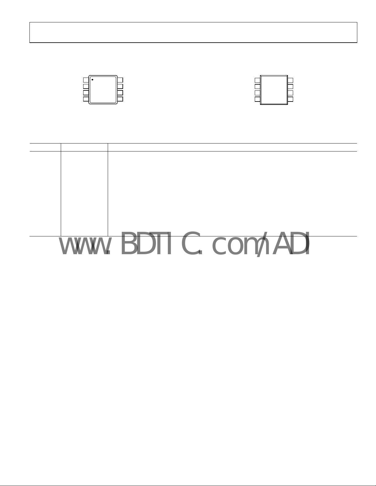
8-lead SOIC and MSOP packages
Supply current: 2.6 mA maximum
Supply range: ±2.5 V to ±18 V
APPLICATIONS
ADC driver
High performance audio
Instrumentation amplifier building blocks
Level translators
Automatic test equipment
Sine/cosine encoders
Precision Difference Amplifier
AD8274
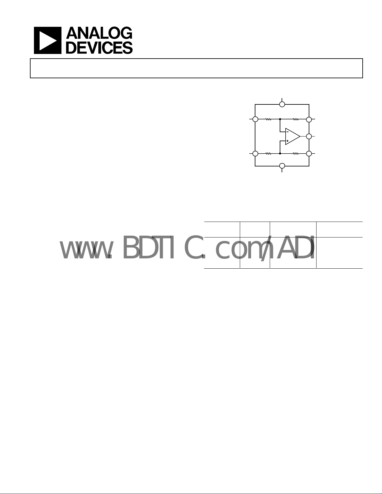
FUNCTIONAL BLOCK DIAGRAM
+
S
7
12kΩ 6kΩ
2
12kΩ
3 1
4
–V
S
Figure 1.
Table 1. Difference Amplifiers by Category
Low
Distortion
AD8270 AD628 AD8202 AD8205
AD8273 AD629 AD8203 AD8206
AD8274 AD8216
AMP03
High
Voltage
Single-Supply
Unidirectional
6kΩ
5
6
07362-001
Single-Supply
Bidirectional
GENERAL DESCRIPTION
The AD8274 is a difference amplifier that delivers excellent ac
and dc performance. Built on Analog Devices, Inc., proprietary
iPolar® process and laser-trimmed resistors, AD8274 achieves a
breakthrough in distortion vs. current consumption and has
excellent gain drift, gain accuracy, and CMRR.
Distortion in the audio band is an extremely low 0.00025%
(112 dB) at a gain of ½ and 0.00035% (109 dB) at a gain of 2
while driving a 600 load
With supply voltages up to ±18 V (+36 V single supply), the
AD8274 is well suited for measuring large industrial signals.
Additionally, the part’s resistor divider architecture allows it to
measure voltages beyond the supplies.
Rev. 0
Information furnished by Analog Devices is believed to be accurate and reliable. However, no
responsibility is assumed by Analog Devices for its use, nor for any infringements of patents or other
rights of third parties that may result from its use. Specifications subject to change without notice. No
license is granted by implication or otherwise under any patent or patent rights of Analog Devices.
Trademarks and registered trademarks are the property of their respective owners.
With no external components, the AD8274 can be configured
as a G = ½ or G = 2 difference amplifier. For single-ended
applications that need high gain stability or low distortion
performance, the AD8274 can also be configured for several
gains ranging from −2 to +3.
The excellent distortion and dc performance of the AD8274,
along with its high slew rate and bandwidth, make it an excellent
ADC driver. Because of the part’s high output drive, it also
makes a very good cable driver.
The AD8274 only requires 2.6 mA maximum supply current. It
is specified over the industrial temperature range of −40°C to
+85°C and is fully RoHS compliant. For the dual version, see the
AD8273 data sheet.
One Technology Way, P.O. Box 9106, Norwood, MA 02062-9106, U.S.A.
Tel: 781.329.4700 www.analog.com
Fax: 781.461.3113 ©2008 Analog Devices, Inc. All rights reserved.

AD8274
www.BDTIC.com/ADI
TABLE OF CONTENTS
Features .............................................................................................. 1
Applications ....................................................................................... 1
Functional Block Diagram .............................................................. 1
General Description ......................................................................... 1
Revision History ............................................................................... 2
Specifications ..................................................................................... 3
Absolute Maximum Ratings ............................................................ 4
Thermal Resistance ...................................................................... 4
Maximum Power Dissipation ..................................................... 4
Short-Circuit Current .................................................................. 4
ESD Caution .................................................................................. 4
REVISION HISTORY
7/08—Revision 0: Initial Version
Pin Configurations and Function Description ..............................5
Typical Performance Characteristics ..............................................6
Theory of Operation ...................................................................... 12
Circuit Information .................................................................... 12
Driving the AD8274 ................................................................... 12
Power Supplies ............................................................................ 12
Input Voltage Range ................................................................... 12
Configurations ............................................................................ 13
Driving Cabling .......................................................................... 14
Outline Dimensions ....................................................................... 15
Ordering Guide .......................................................................... 15
Rev. 0 | Page 2 of 16

AD8274
www.BDTIC.com/ADI
SPECIFICATIONS
VS = ±15 V, V
Table 2.
G = ½ G = 2
Parameter Conditions Min Typ Max Min Typ Max Unit
DYNAMIC PERFORMANCE
Bandwidth 20 10 MHz
Slew Rate 20 20 V/μs
Settling Time to 0.1% 10 V step on output, CL = 100 pF 650 750 675 775 ns
Settling Time to 0.01% 10 V step on output, CL = 100 pF 725 800 750 825 ns
NOISE/DISTORTION
THD + Noise
Noise Floor, RTO
Output Voltage Noise
(Referred to Output)
f = 1 kHz 26 52 nV/√Hz
GAIN
Gain Error 0.03 0.03 %
Gain Drift −40°C to +85°C 0.5 2 0.5 2 ppm/°C
Gain Nonlinearity V
INPUT CHARACTERISTICS
3
Offset
vs. Temperature −40°C to +85°C 3 6 μV/°C
vs. Power Supply VS = ±2.5 V to ±18 V 5 10 μV/V
Common-Mode Rejection Ratio
Input Voltage Range
Impedance
Differential VCM = 0 V 24 12 kΩ
Common Mode
OUTPUT CHARACTERISTICS
Output Swing
Short-Circuit Current Limit Sourcing 90 90 mA
Sinking 60 60 mA
Capacitive Load Drive 200 1200 pF
POWER SUPPLY
Supply Current (per Amplifier) 2.3 2.6 2.3 2.6 mA
TEMPERATURE RANGE
Specified Performance −40 +85 −40 +85 °C
1
Includes amplifier voltage and current noise, as well as noise of internal resistors.
2
dBu = 20 log(V rms/0.7746).
3
Includes input bias and offset current errors.
4
May also be limited by absolute maximum input voltage or by the output swing. See the Absolute Maximum Ratings section and Figure 8 through Figure 11 for details.
5
Internal resistors are trimmed to be ratio matched but to have ±20% absolute accuracy.
6
Common mode is calculated by looking into both inputs. The common-mode impedance at only one input is 18 kΩ.
= 0 V, TA = 25°C, RL = 2 kΩ, unless otherwise noted.
REF
1
f = 1 kHz, V
= 10 V p-p,
OUT
0.00025 0.00035 %
600 Ω load
2
20 kHz BW −106 −100 dBu
f = 20 Hz to 20 kHz 3.5 7 μV rms
= 10 V p-p, 600 Ω load 2 2 ppm
OUT
Referred to output 150 700 300 1100 μV
= ±40 V, RS = 0 Ω, referred
V
CM
77 86 83 92 dB
to input
4
−3V
+ 4.5
5
6
9 9 kΩ
−V
1.5
S
+
S
+3VS
− 4.5
+V
S
1.5
−
−1.5VS
+ 2.3
−VS +
1.5
+1.5VS
V
− 2.3
+V
S
−
V
1.5
Rev. 0 | Page 3 of 16

AD8274
www.BDTIC.com/ADI
ABSOLUTE MAXIMUM RATINGS
Table 3.
Parameter Rating
Supply Voltage ±18 V
Maximum Voltage at Any Input Pin −VS + 40 V
Minimum Voltage at Any Input Pin +VS – 40 V
Storage Temperature Range −65°C to +150°C
Specified Temperature Range −40°C to +85°C
Package Glass Transition Temperature (TG) 150°C
Stresses above those listed under Absolute Maximum Ratings
may cause permanent damage to the device. This is a stress
rating only; functional operation of the device at these or any
other conditions above those indicated in the operational
section of this specification is not implied. Exposure to absolute
maximum rating conditions for extended periods may affect
device reliability.
THERMAL RESISTANCE
The θJA values in Tabl e 4 assume a 4-layer JEDEC standard
board with zero airflow.
MAXIMUM POWER DISSIPATION
The maximum safe power dissipation for the AD8274 is limited
by the associated rise in junction temperature (T
approximately 150°C, which is the glass transition temperature,
the properties of the plastic change. Even temporarily exceeding
this temperature limit may change the stresses that the package
exerts on the die, permanently shifting the parametric performance
of the amplifiers. Exceeding a temperature of 150°C for an
extended period may result in a loss of functionality.
2.0
TJ MAX = 150°C
1.6
1.2
MSOP
θ
= 135°C/W
0.8
0.4
MAXIMUM POWER DISSIPATIO N (W)
JA
SOIC
= 121°C/W
θ
JA
) on the die. At
J
Table 4. Thermal Resistance
Package Type θJA Unit
8-Lead MSOP 135 °C/W
8-Lead SOIC 121 °C/W
0
–50 0–25 25 50 75 100 125
Figure 2. Maximum Power Dissipation vs. Ambient Temperature
AMBIENT TEM ERATURE (°C)
07362-004
SHORT-CIRCUIT CURRENT
The AD8274 has built-in, short-circuit protection that limits the
output current (see Figure 16 for more information). While the
short-circuit condition itself does not damage the part, the heat
generated by the condition can cause the part to exceed its
maximum junction temperature, with corresponding negative
effects on reliability. Figure 2 and Figure 16, combined with
knowledge of the part’s supply voltages and ambient temperature,
can be used to determine whether a short circuit will cause the
part to exceed its maximum junction temperature.
ESD CAUTION
Rev. 0 | Page 4 of 16
AD8274
www.BDTIC.com/ADI
PIN CONFIGURATIONS AND FUNCTION DESCRIPTION
REF
1
AD8274
2
–IN
TOP VIEW
+IN
3
(Not to Scal e)
–V
4
S
NC = NO CONNECT
Figure 3. MSOP Pin Configuration
Table 5. Pin Function Descriptions
Pin No. Mnemonic Description
1 REF
2 −IN
3 +IN
4 −VS Negative Supply.
5 SENSE
6 OUT Output.
7 +VS Positive Supply.
8 NC No Connect.
NC
8
7
6
5
+V
S
OUT
SENSE
07362-002
REF
1
–IN
2
+IN
3
(Not to Scale)
4
–V
S
NC = NO CONNECT
AD8274
TOP VIEW
8
7
6
5
NC
+V
S
OUT
SENSE
07362-003
Figure 4. SOIC Pin Configuration
6 kΩ Resistor to Noninverting Terminal of Op Amp. Used as reference pin in G = ½ configuration. Used as
positive input in G = 2 configuration.
12 kΩ Resistor to Inverting Terminal of Op Amp. Used as negative input in G = ½ configuration. Connect
to output in G = 2 configuration.
12 kΩ Resistor to Noninverting Terminal of Op Amp. Used as positive input in G = ½ configuration. Used
as reference pin in G = 2 configuration.
6 kΩ Resistor to Inverting Terminal of Op Amp. Connect to output in G = ½ configuration. Used as
negative input in G = 2 configuration.
Rev. 0 | Page 5 of 16

AD8274
www.BDTIC.com/ADI
TYPICAL PERFORMANCE CHARACTERISTICS
VS = ±15 V, TA = 25°C, gain = ½, difference amplifier configuration, unless otherwise noted.
20
15
10
5
0
–5
CMR (µV/V)
–10
–15
–20
–25
REPRESENTATIVE SAMPLES
–30
–50 –30 10 50 130
–10 30 70 90 110
TEMPERATURE ( °C)
Figure 5. CMR vs. Temperature, Normalized at 25°C, Gain = ½
07362-106
25
20
15
10
–13.5V, +11. 5V
5
0
–5
–13.5V, –11.5V
–10
–15
INPUT COMMON-MODE VO LTAGE (V)
–20
–25
–15 –10 –5 0 5 10 15
0V, +20.85V
VS = ±15V
0V, –20.85V
OUTPUT VO LTAGE (V)
G = 2
+13.5V, + 11.5V
+13.5V, –11. 5V
Figure 8. Input Common-Mode Voltage vs. Output Voltage,
Gain = ½, ±15 V Supplies
07362-111
150
100
50
0
–50
SYSTEM OFFSET (µV)
–100
–150
REPRESENTATIVE SAMPLES
–200
–50 –30 10 50 130
–10 30 70 90 110
TEMPERATURE ( °C)
Figure 6. System Offset vs. Temperature, Normalized at 25°C,
Referred to Output, Gain = ½
30
20
10
0
–10
20
–3.5V, +15. 8V
15
10
5
0
–5
–10
INPUT COMMON-MODE VOLTAGE (V)
–15
07362-107
–20
–4–3–2–101234
–1.0V, +6. 2V
–1.0V, –4. 0V
–3.5V, –8.7V
VS = ±5V
VS = ±2.5V
+1.0V, +4.2V
+1.0, –6.0V
OUTPUT VO LTAGE (V)
G = ½
+3.5V, +8.8V
+3.5V, –15. 5V
07362-110
Figure 9. Input Common-Mode Voltage vs. Output Voltage,
Gain = ½, ±5 V and ±2.5 V Supplies
3
0
2
0
1
0
0
0V, +25V
VS = ±15V
–13.5V, +11. 5V
G = ½
+13.5V, +11. 5V
–20
GAIN ERROR (µ V/V)
–30
–40
REPRESENTATIVE SAMPLES
–50
–50 –30 10 50 130
–10 30 70 90 110
TEMPERATURE ( °C)
Figure 7. Gain Error vs. Temperature, Normalized at 25°C, Gain = ½
INPUT COMMON-MODE VOLTAGE (V)
07362-108
–13.5V, –11.5V
–
1
0
–
2
0
–
3
0
–15 –10 –5 0 5 10 15
OUTPUT VO LTAGE (V)
Figure 10. Input Common-Mode Voltage vs. Output Voltage,
Gain = 2, ±15 V Supplies
Rev. 0 | Page 6 of 16
0V, –25V
+13.5V, –11. 5V
07362-210

AD8274
www.BDTIC.com/ADI
8
–3.5V, +6. 9V
6
4
2
0
–2
–4
INPUT COMMON-MODE VOL TAGE (V)
–6
–8
–4–3–2–101234
–1.0V, +2. 7V
–1.0V, –2. 0V
–3.5V, –5.2V
VS = ±5V
VS = ±2.5V
OUTPUT VOLTAGE (V)
+1.0V, +2.2V
Figure 11. Input Common-Mode Voltage vs. Output Voltage,
Gain = 2, ±5 V and ±2.5 V Supplies
140
POSITIVE PSRR
120
100
NEGATIVE PS RR
80
60
40
POWER SUPPL Y REJECTIO N (dB)
20
+3.5V, +5. 2V
+1.0, –2.6V
G = 2
+3.5V, –6. 9V
10
G = 2
5
0
–5
GAIN (dB)
–10
–15
07362-112
–20
1k100 10k 100k 1M 100M10M
G = ½
FREQUENCY(Hz)
07362-007
Figure 14. Gain vs. Frequency
120
100
80
60
CMRR (dB)
40
20
GAIN = 2
GAIN = ½
0
100 1M100k10k1k110
FREQUENCY (Hz)
Figure 12. Power Supply Rejection Ratio vs. Frequency,
Gain = ½, Referred to Output
32
±15V SUPPLY
28
24
20
16
12
±5V SUPPLY
8
MAXIMUM OUTPUT VOLTAGE (V p-p)
4
0
1k100 10k 100k 1M 10M
FREQUENCY (Hz)
Figure 13. Maximum Output Voltage vs. Frequency
0
07362-021
1k10010 10k 100k 1M
FREQUENCY (Hz)
7362-217
Figure 15. Common-Mode Rejection Ratio vs. Frequency, Referred to Input
120
100
80
60
40
20
0
–20
–40
SHORT-CIRCUIT CURRENT (mA)
–60
–80
–100
–40 –20 20 60
7362-006
04080100 120
TEMPERATURE ( °C)
SOURCING
SINKING
07362-117
Figure 16. Short-Circuit Current vs. Temperature
Rev. 0 | Page 7 of 16

AD8274
V
V
www.BDTIC.com/ADI
+
+VS– 2
+V
–V
OUTPUT VOLT AGE SWING (V)
–V
+VS – 3
+V
S
+125° C
–40°C
– 4
S
0
+ 2
S
+ 4
S
–V
S
–40°C
+125°C
+25°C
+85°C
Figure 17. Output Voltage Swing vs. RL, VS = ±15 V
+
S
– 6
S
+85°C
+25°C
1k200 10k
LOAD RESIST ANCE (Ω)
–40°C
+125°C
+25°C
+85°C
CL = 100pF
50mV/DIV
07362-009
600Ω
NO LOAD
2kΩ
1µs/DIV
07362-025
Figure 20. Small-Signal Step Response, Gain = ½
NO LOAD
2kΩ
+125°C
CURRENT (mA)
1µs/DIV
+85°C
+25°C
–40°C
OUT
–VS + 6
OUTPUT VOLTAGE (V)
–V
+ 3
S
–V
S
0 2040608010
Figure 18. Output Voltage vs. I
CL = 100pF
50mV/DIV
600Ω
Figure 19. Small-Signal Step Response, Gain = 2
0
7362-023
07362-024
50mV/DIV
1µs/DIV
07362-026
Figure 21. Small-Signal Pulse Response with 500 pF Capacitor Load,
Gain = 2
50mV/DIV
1µs/DIV
7362-027
Figure 22. Small-Signal Pulse Response for 100 pF Capacitive Load,
Gain = ½
Rev. 0 | Page 8 of 16

AD8274
www.BDTIC.com/ADI
100
90
80
70
60
50
40
OVERSHOOT (%)
30
20
10
0
0 2 0 40 60 80 100 120 140 160 180 200
CAPACI TIVE LOAD (pF)
2.5V
5V
15V
18V
Figure 23. Small-Signal Overshoot vs. Capacitive Load,
Gain = ½, No Resistive Load
100
90
80
70
60
50
40
OVERSHOOT (%)
30
20
10
0
0 2 0 40 60 80 100 120 140 160 180 200
CAPACI TIVE LOAD (pF)
2.5V
5V
15V
18V
Figure 24. Small-Signal Overshoot vs. Capacitive Load,
Gain = ½, 600 Ω in Parallel with Capacitive Load
07362-037
07362-038
100
90
80
70
60
50
40
OVERSHOOT (%)
30
20
10
0
0 200 400 600 800 1000 1200
CAPACITIVE L OAD (pF)
18V
2.5V
Figure 26. Small-Signal Overshoot vs. Capacitive Load,
Gain = 2, 600 Ω in Parallel with Capacitive Load
2V/DIV
1µs/DIV
Figure 27. Large-Signal Pulse Response,
Gain = ½
15V
5V
07362-040
07362-032
100
90
80
70
60
50
40
OVERSHOOT (%)
30
20
10
0
0 200 400 600 800 1000 1200
CAPACITIVE LOAD (pF)
Figure 25. Small-Signal Overshoot vs. Capacitive Load,
18V
2.5V
5V
15V
2V/DIV
07362-039
Figure 28. Large-Signal Pulse Response,
Gain = 2, No Resistive Load
Rev. 0 | Page 9 of 16
1µs/DIV
Gain = 2
07362-033

AD8274
www.BDTIC.com/ADI
40
35
30
25
+SR
20
–SR
15
SLEW RATE (V/µS)
10
5
0
–40 –20 0 20 40 60 80 100 120
TEMPERATURE ( °C)
Figure 29. Slew Rate vs. Temperature
10k
1k
7362-010
0.1
22kHz FILTER
V
= 10V p-p
OUT
R
= 600Ω
L
0.01
THDN + N (%)
0.001
GAIN = 2
GAIN = ½
0.0001
10
100
FREQUENCY (Hz)
1k 10k
Figure 32. THD + N vs. Frequency, Filter = 22k Hz
0.1
V
= 10V p-p
OUT
0.01
100k
07362-131
100
VOLTAGE NOISE DENSITY (nV/ √Hz)
10
GAIN = 2
GAIN = ½
1 10 100 1k 10k 100k
FREQUENCY (Hz)
Figure 30. Voltage Noise Density vs. Frequency, Referred to Output
G = 2
1µV/DIV
G = ½
1s/DIV
Figure 31. 0.1 Hz to 10 Hz Voltage Noise, RTO
THD + N (%)
0.001
0.0001
07362-034
GAIN = 2
GAIN = ½
10
100
1k 10k
FREQUENCY (Hz)
100k
07362-135
Figure 33. THD + N vs. Frequency, Filter = 120 kHz
1
GAIN = ½
f = 1kHz
0.1
R
= 2kΩ, 100Ω
0.01
THD + N (%)
0.001
0.0001
07362-035
0
10 15
OUTPUT AMPL ITUDE (dBu)
L
RL = 600Ω
20
255
7362-136
Figure 34. THD + N vs. Output Amplitude, G = ½
Rev. 0 | Page 10 of 16

AD8274
www.BDTIC.com/ADI
0.1
1
GAIN = 2
f = 1kHz
0.1
0.01
GAIN = 2
V
= 10V p-p
OUT
0.01
THD + N (%)
0.001
0.0001
= 600Ω
R
L
R
= 2kΩ
L
R
= 100kΩ
L
0
10 15
OUTPUT AMPL ITUDE (dBu)
Figure 35. THD + N vs. Output Amplitude, G = 2
0.1
GAIN = ½
V
= 10V p-p
OUT
0.01
0.001
THIRD HARMONIC ALL LOADS
0.0001
SECOND HARMONIC RL = 600Ω
AMPLITUDE ( % OF FUNDAMENT AL)
0.00001
SECOND HARMONIC RL = 100kΩ, 2kΩ
10
100
FREQUENCY (Hz)
1k 10k
Figure 36. Harmonic Distortion Products vs. Frequency, G = ½
0.001
THIRD HARMONIC ALL LOADS
0.0001
SECOND HARMONIC RL = 600Ω
AMPLITUDE ( % OF FUNDAMENT AL)
20
255
7362-137
0.00001
SECOND HARMONIC RL = 100kΩ, 2kΩ
10
100
FREQUENCY (Hz)
1k 10k
100k
07362-139
Figure 37. Harmonic Distortion Products vs. Frequency, G = 2
100k
07362-138
Rev. 0 | Page 11 of 16

AD8274
V
www.BDTIC.com/ADI
THEORY OF OPERATION
+
S
7
12kΩ 6kΩ
2
12kΩ
3 1
4
–V
S
Figure 38. Functional Block Diagram
CIRCUIT INFORMATION
The AD8274 consists of a high precision, low distortion op amp
and four trimmed resistors. These resistors can be connected to
make a wide variety of amplifier configurations, including
difference, noninverting, and inverting configurations. Using
the on-chip resistors of the AD8274 provides the designer with
several advantages over a discrete design.
DC Performance
Much of the dc performance of op amp circuits depends on the
accuracy of the surrounding resistors. The resistors on the AD8274
are laid out to be tightly matched. The resistors of each part are
laser trimmed and tested for their matching accuracy. Because
of this trimming and testing, the AD8274 can guarantee high
accuracy for specifications such as gain drift, common-mode
rejection, and gain error.
AC Performance
Because feature size is much smaller in an integrated circuit than
on a printed circuit board (PCB), the corresponding parasitics are
also smaller. The smaller feature size helps the ac performance of
the AD8274. For example, the positive and negative input terminals
of the AD8274 op amp are not pinned out intentionally. By not
connecting these nodes to the traces on the PCB, the capacitance
remains low, resulting in both improved loop stability and
common-mode rejection over frequency.
Production Costs
Because one part, rather than several, is placed on the PCB, the
board can be built more quickly.
Size
The AD8274 fits a precision op amp and four resistors in one
8-lead MSOP or SOIC package.
6kΩ
5
6
07362-001
DRIVING THE AD8274
The AD8274 is easy to drive, with all configurations presenting
at least several kilohms (kΩ) of input resistance. The AD8274
should be driven with a low impedance source: for example,
another amplifier. The gain accuracy and common-mode rejection
of the AD8274 depend on the matching of its resistors. Even
source resistance of a few ohms can have a substantial effect on
these specifications.
POWER SUPPLIES
A stable dc voltage should be used to power the AD8274. Noise
on the supply pins can adversely affect performance. A bypass
capacitor of 0.1 µF should be placed between each supply pin
and ground, as close as possible to each supply pin. A tantalum
capacitor of 10 µF should also be used between each supply and
ground. It can be farther away from the supply pins and, typically,
it can be shared by other precision integrated circuits.
The AD8274 is specified at ±15 V, but it can be used with
unbalanced supplies, as well. For example, −V
= 0 V, +VS = 20 V.
S
The difference between the two supplies must be kept below 36 V.
INPUT VOLTAGE RANGE
The AD8274 can measure voltages beyond the rails. For the G = ½
and G = 2 difference amplifier configurations, see the input voltage
range in Tab l e 2 for specifications.
The AD8274 is able to measure beyond the rail because the
internal resistors divide down the voltage before it reaches the
internal op amp. Figure 39 shows an example of how the voltage
division works in the difference amplifier configuration. For the
AD8274 to measure correctly, the input voltages at the internal
op amp must stay within 1.5 V of either supply rail.
R2
(V
)
IN+
R1 + R2
R4
R3
R1
R2
R2
(V
)
IN+
R1 + R2
Figure 39. Voltage Division in the Difference Amplifier Configuration
For best long-term reliability of the part, voltages at any of the
part’s inputs (Pin 1, Pin 2, Pin 3, or Pin 5) should stay within
+V
– 40 V to −VS + 40 V. For example, on ±10 V supplies,
S
input voltages should not exceed ±30 V.
07362-061
Rev. 0 | Page 12 of 16

AD8274
V
V
V
V
+
www.BDTIC.com/ADI
CONFIGURATIONS
The AD8274 can be configured in several ways; see Figure 40 to Figure 47. Because these configurations rely on the internal, matched
resistors, all of these configurations have excellent gain accuracy and gain drift. Note that the AD8274 internal op amp is stable for noise
gains of 1.5 and higher, so the AD8274 should not be placed in a unity-gain follower configuration.
–IN
+IN
V
OUT
12kΩ
2
12kΩ 6kΩ
3
= ½ (V
IN+
− V
6kΩ
5
OUT
6
1
)
IN−
Figure 40. Difference Amplifier, G = ½
–IN
+IN
OUT
6kΩ
5
6kΩ 12kΩ
1
= 2 (V
IN+
− V
12kΩ
2
OUT
6
3
)
IN−
Figure 41. Difference Amplifier, G = 2
–IN
12kΩ
2
6kΩ
1
12kΩ
3
V
= –½ V
OUT
6kΩ
5
OUT
6
IN
Figure 42. Inverting Amplifier, G = −½
12kΩ
2
12kΩ 6kΩ
3
+IN
07362-012
OUT
= ½ V
IN
6kΩ
5
OUT
6
1
07362-015
Figure 44. Noninverting Amplifier, G = ½
6kΩ
5
6kΩ 12kΩ
1
07362-016
+IN
OUT
= 2 V
IN
12kΩ
2
OUT
6
3
07362-019
Figure 45. Noninverting Amplifier, G = 2
12kΩ
25
6kΩ
1
IN
12kΩ
3
07362-013
V
= 1½ V
OUT
Figure 46. Noninverting Amplifier, G = 1.5
6kΩ
OUT
6
IN
07362-014
6kΩ
5
–IN
12kΩ
1
6kΩ
3
= –2 V
OUT
IN
Figure 43. Inverting Amplifier, G = −2
12kΩ
2
OUT
6
+IN
V
= 3 V
07362-017
OUT
Figure 47. Noninverting Amplifier, G = 3
Rev. 0 | Page 13 of 16
6kΩ
5
12kΩ
3
6kΩ
1
IN
12kΩ
2
OUT
6
07362-018

AD8274
www.BDTIC.com/ADI
DRIVING CABLING
Because the AD8274 can drive large voltages at high output
currents and slew rates, it makes an excellent cable driver. It is
good practice to put a small value resistor between the AD8274
output and cable, since capacitance in the cable can cause peaking
or instability in the output response. A resistance of 20 or higher
is recommended.
AD8274
Figure 48. Driving Cabling
R ≥ 20Ω
06979-060
Rev. 0 | Page 14 of 16

AD8274
www.BDTIC.com/ADI
OUTLINE DIMENSIONS
5.00 (0.1968)
4.80 (0.1890)
4.00 (0.1574)
3.80 (0.1497)
0.25 (0.0098)
0.10 (0.0040)
COPLANARITY
0.10
CONTROLL ING DIMENSI ONS ARE IN MILLIMETERS; INCH DI MENSIONS
(IN PARENTHESES) ARE ROUNDED-OFF MILLIMETER EQUIVALENTS FOR
REFERENCE ONLY AND ARE NOT APPROPRI ATE FOR USE IN DESIGN.
85
1
1.27 (0.0500)
SEATING
PLANE
COMPLIANT TO JEDEC STANDARDS MS-012-A A
BSC
6.20 (0.2441)
5.80 (0.2284)
4
1.75 (0.0688)
1.35 (0.0532)
0.51 (0.0201)
0.31 (0.0122)
8°
0°
0.25 (0.0098)
0.17 (0.0067)
0.50 (0.0196)
0.25 (0.0099)
1.27 (0.0500)
0.40 (0.0157)
45°
012407-A
Figure 49. 8-Lead Standard Small Outline Package [SOIC_N]
Narrow Body (R-8)
Dimensions shown in millimeters and (inches)
3.20
3.00
2.80
8
5
4
SEATING
PLANE
5.15
4.90
4.65
1.10 MAX
0.23
0.08
8°
0°
0.80
0.60
0.40
3.20
3.00
2.80
PIN 1
0.95
0.85
0.75
0.15
0.00
COPLANARITY
1
0.65 BSC
0.38
0.22
0.10
COMPLIANT TO JEDEC STANDARDS MO-187-AA
Figure 50. 8-Lead Mini Small Outline Package [MSOP]
(RM-8)
Dimensions shown in millimeters
ORDERING GUIDE
Model Temperature Range Package Description Package Option Branding
AD8274ARZ
AD8274ARZ-R7
AD8274ARZ-RL
AD8274ARMZ
AD8274ARMZ-R7
AD8274ARMZ-RL
1
Z = RoHS Compliant Part.
1
−40°C to +85°C 8-Lead SOIC_N R-8
1
−40°C to +85°C 8-Lead SOIC_N, 7" Tape and Reel R-8
1
−40°C to +85°C 8-Lead SOIC_N, 13" Tape and Reel R-8
1
−40°C to +85°C 8-Lead MSOP RM-8 Y1B
1
−40°C to +85°C 8-Lead MSOP, 7" Tape and Reel RM-8 Y1B
1
−40°C to +85°C 8-Lead MSOP, 13" Tape and Reel RM-8 Y1B
Rev. 0 | Page 15 of 16

AD8274
www.BDTIC.com/ADI
NOTES
©2008 Analog Devices, Inc. All rights reserved. Trademarks and
registered trademarks are the property of their respective owners.
D07362-0-7/08(0)
Rev. 0 | Page 16 of 16
 Loading...