

Dual-Channel,
V
www.BDTIC.com/ADI
FEATURES
Two gain settings
Gain of ½ (−6 dB)
Gain of 2 (+6 dB)
0.05% maximum gain error
10 ppm maximum gain drift
Excellent ac specifications
20 V/μs minimum slew rate
800 ns to 0.01% settling time
Low distortion: 0.004%, 20 Hz to 20 kHz
High accuracy dc performance
77 dB minimum CMRR
700 μV maximum offset voltage
14-lead SOIC package
Supply current: 2.5 mA maximum per channel
Supply range: ±2.5 V to ±18 V
APPLICATIONS
High performance audio
Instrumentation amplifier building blocks
Level translators
Automatic test equipment
Sin/Cos encoders
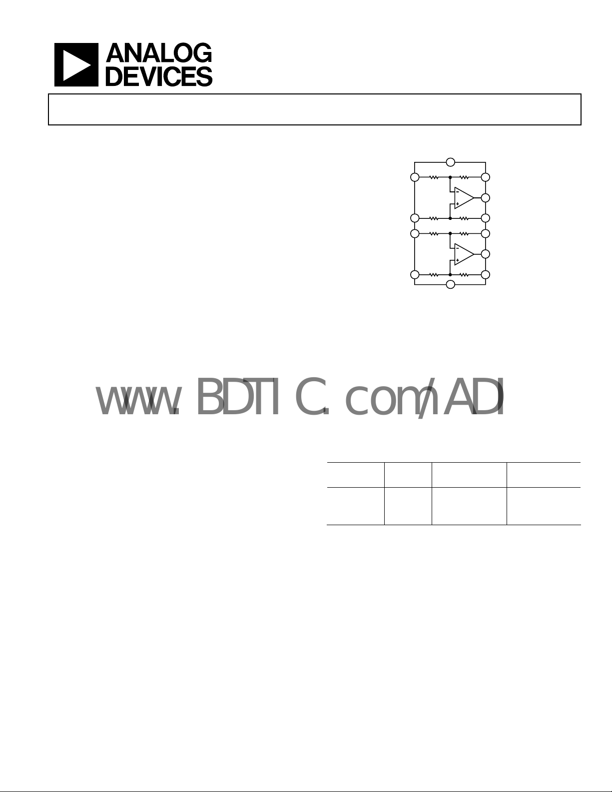
GENERAL DESCRIPTION
The AD8273 is a low distortion, dual-channel amplifier with
internal gain setting resistors. With no external components,
it can be configured as a high performance difference amplifier
(G = ½ or 2), inverting amplifier (G = ½ or 2), or noninverting
amplifier (G = 1½ or 3).
The AD8273 operates on both single and dual supplies and only
r
equires 2.5 mA maximum supply current for each amplifier.
It is specified over the industrial temperature range of −40°C to
+85°C and is fully RoHS compliant.
Audio Difference Amplifier
AD8273
FUNCTIONAL BLOCK DIAGRAM
+
S
11
12kΩ
2
12kΩ
3
12kΩ
6
12kΩ
58
Table 1. Difference Amplifiers by Category
Low
Distortion
High
Voltage
AD8270 AD628 AD8202 AD8205
AD8273 AD629 AD8203 AD8206
AMP03 AD8216
6kΩ
12
13
6kΩ
14
6kΩ
10
9
6kΩ
4
–V
S
Figure 1.
Single-Supply
Unidirectional
06981-001
Single-Supply
Bidirectional
Rev. 0
Information furnished by Analog Devices is believed to be accurate and reliable. However, no
responsibility is assumed by Anal og Devices for its use, nor for any infringements of patents or ot her
rights of third parties that may result from its use. Specifications subject to change without notice. No
license is granted by implication or otherwise under any patent or patent rights of Analog Devices.
Trademarks and registered trademarks are the property of their respective owners.
One Technology Way, P.O. Box 9106, Norwood, MA 02062-9106, U.S.A.
Tel: 781.329.4700 www.analog.com
Fax: 781.461.3113 ©2008 Analog Devices, Inc. All rights reserved.

AD8273
www.BDTIC.com/ADI
TABLE OF CONTENTS
Features.............................................................................................. 1
Applications....................................................................................... 1
General Description ......................................................................... 1
Functional Block Diagram .............................................................. 1
Revision History ............................................................................... 2
Specifications..................................................................................... 3
Absolute Maximum Ratings............................................................ 4
Maximum Power Dissipation..................................................... 4
ESD Caution.................................................................................. 4
REVISION HISTORY
1/08—Revision 0: Initial Version
Pin Configuration and Function Descriptions..............................5
Typical Performance Characteristics..............................................6
Theory of Operation ...................................................................... 11
Configurations............................................................................ 11
Power Supplies............................................................................ 11
Outline Dimensions....................................................................... 13
Ordering Guide .......................................................................... 13
Rev. 0 | Page 2 of 16
AD8273
www.BDTIC.com/ADI
SPECIFICATIONS
VS = ±15 V, V
Table 2.
Parameter Conditions Min Typ Max Unit
DYNAMIC PERFORMANCE
Bandwidth 20 MHz
Slew Rate 20 V/μs
Settling Time to 0.1% 10 V step on output, CL = 100 pF 670 750 ns
Settling Time to 0.01% 10 V step on output, CL = 100 pF 750 800 ns
Channel Separation f = 1 kHz 130 dB
NOISE/DISTORTION
THD + Noise f = 1 kHz, V
Noise Floor, RTO
Output Voltage Noise (Referred to Output) f = 20 Hz to 20 kHz 3.5 μV rms
f = 1 kHz 26 nV/√Hz
GAIN
Gain Error 0.05 %
Gain Drift −40°C to +85°C 2 10 ppm/°C
Gain Nonlinearity V
V
INPUT CHARACTERISTICS
3
Offset
vs. Temperature −40°C to +85°C 3 μV/°C
vs. Power Supply VS = ±2.5 V to ±18 V 2 10 μV/V
Common-Mode Rejection Ratio VCM = ±40 V, RS = 0 Ω, referred to input 77 86 dB
Input Voltage Range
Impedance
Differential VCM = 0 V 36 kΩ
Common Mode
OUTPUT CHARACTERISTICS
Output Swing −VS + 1.5 +VS − 1.5 V
Short-Circuit Current Limit Sourcing 100 mA
Sinking 60 mA
Capacitive Load Drive G = ½ 200 pF
G = 2 1200 pF
POWER SUPPLY
Supply Current (per Amplifier) 2.5 mA
TEMPERATURE RANGE
Specified Performance −40 +85 °C
1
Includes amplifier voltage and current noise, as well as noise of internal resistors.
2
dBu = 20 log (V rms /0.7746).
3
Includes input bias and offset current errors.
4
May also be limited by absolute maximum input voltage or by the output swing. See the Absolute Maximum Ratings section and Figure 9 through Figure 12 for
details.
5
Internal resistors are trimmed to be ratio matched but have ±20% absolute accuracy.
6
Common mode is calculated looking into both inputs. Common-mode impedance looking into only one input is 18 kΩ.
= 0 V, TA = 25°C, G = ½, RL = 2 kΩ, unless otherwise noted.
REF
1
2
= 10 V p-p, 600 Ω load 0.004 %
OUT
20 kHz BW −106 dBu
= 10 V p-p, 600 Ω load 200 ppm
OUT
= 5 V p-p, 600 Ω load 50 ppm
OUT
Referred to output 100 700 μV
4
5
6
−3VS + 4.5 +3VS − 4.5 V
9 kΩ
Rev. 0 | Page 3 of 16
AD8273
www.BDTIC.com/ADI
ABSOLUTE MAXIMUM RATINGS
Table 3.
Parameter Rating
Supply Voltage ±18 V
Output Short-Circuit Current
Voltage at Any Input Pin 40 V
Differential Input Voltage 40 V
Current into Any Input Pin 3 mA
Storage Temperature Range −65°C to +130°C
Specified Temperature Range −40°C to +85°C
Thermal Resistance
θJA 105°C/W
θJC 36°C/W
Package Glass Transition Temperature (TG) 150°C
Observe
ating curve
der
Stresses above those listed under Absolute Maximum Ratings
may cause permanent damage to the device. This is a stress
rating only; functional operation of the device at these or any
other conditions above those indicated in the operational
section of this specification is not implied. Exposure to absolute
maximum rating conditions for extended periods may affect
device reliability.
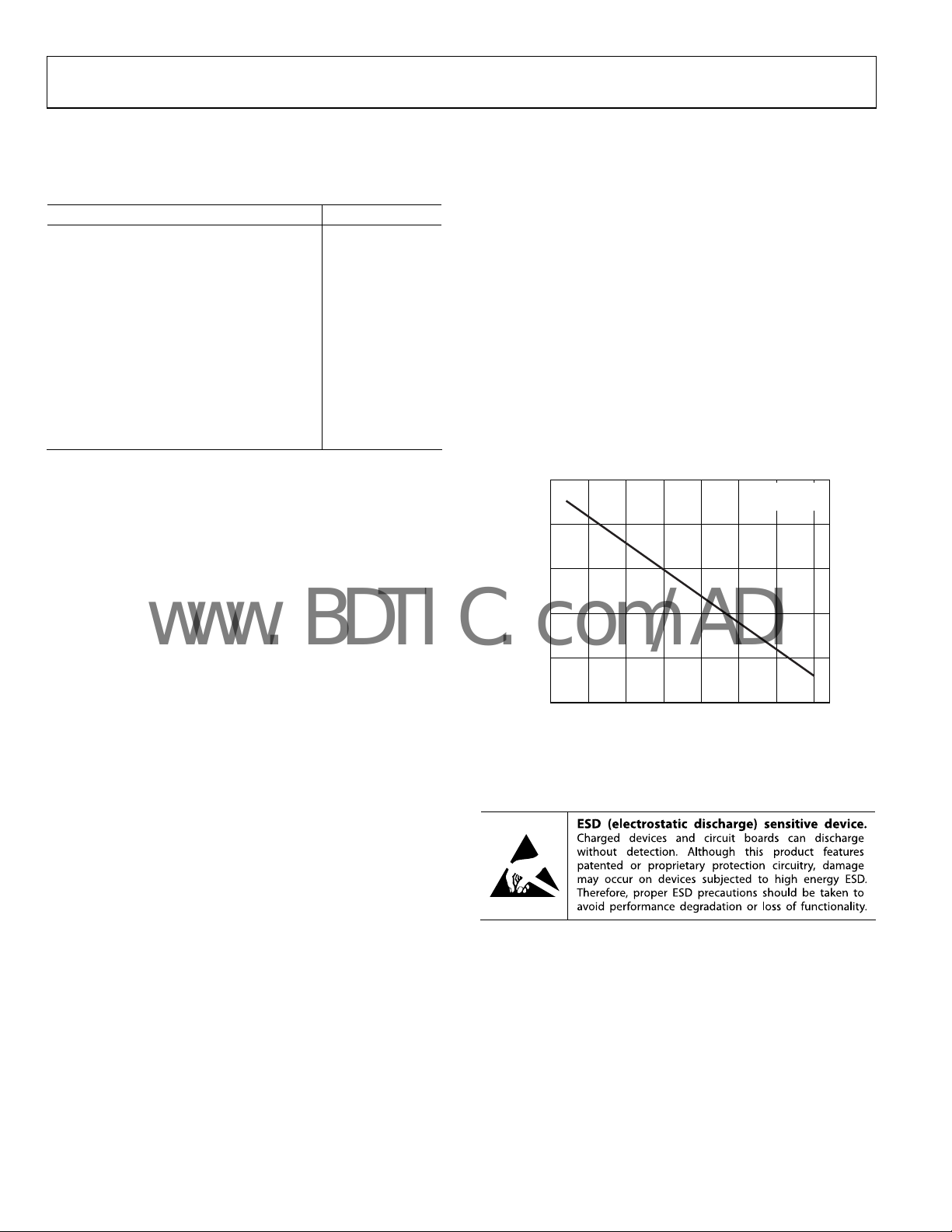
MAXIMUM POWER DISSIPATION
The maximum safe power dissipation for the AD8273 is limited
by the associated rise in junction temperature (T
approximately 150°C, which is the glass transition temperature,
the plastic changes its properties. Even temporarily exceeding
this temperature limit may change the stresses that the package
exerts on the die, permanently shifting the parametric performance
of the amplifiers. Exceeding a temperature of 150°C for an
extended period can result in a loss of functionality.
The AD8273 has built-in, short-circuit p
rotection that limits the
output current to approximately 100 mA (see Figure 2 for more
info
rmation). While the short-circuit condition itself does not
damage the part, the heat generated by the condition can cause
the part to exceed its maximum junction temperature, with
corresponding negative effects on reliability.
2.0
1.6
1.2
) on the die. At
J
TJ MAX = 150°C
θ
= 105°C/W
JA
0.8
0.4
MAXIMUM POWER DISSIPATION (W)
0
–50 –25 0 25 50 75 100 125
AMBIENT TEMPERATURE (°C)
Figure 2. Maximum Power Dissipation vs. Ambient Temperature
06981-043
ESD CAUTION
Rev. 0 | Page 4 of 16
AD8273
www.BDTIC.com/ADI
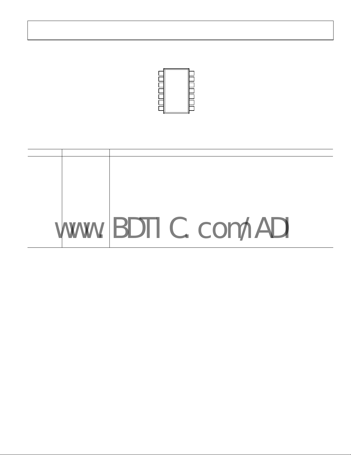
PIN CONFIGURATION AND FUNCTION DESCRIPTIONS
1
NC
2
–12A
+12A
3
–V
4
S
+12B
5
6
–12B
7
NC
NC = NO CONNECT
AD8273
TOP VIEW
(Not to Scale)
14
+6A
13
OUTA
–6A
12
+V
11
S
–6B
10
9
OUTB
8
+6B
06981-020
Figure 3. Pin Configuration
Table 4. Pin Function Descriptions
Pin No. Mnemonic Description
1, 7 NC No Connect.
2 −12A The 12 kΩ resistor connects to the negative terminal of Op Amp A.
3 +12A The 12 kΩ resistor connects to the positive terminal of Op Amp A.
4 −VS Negative Supply.
5 +12B The 12 kΩ resistor connects to the positive terminal of Op Amp B.
6 −12B The 12 kΩ resistor connects to the negative terminal of Op Amp B.
8 +6B The 6 kΩ resistor connects to the positive terminal of Op Amp B.
9 OUTB Op Amp B Output.
10 −6B The 6 kΩ resistor connects to the negative terminal of Op Amp B.
11 +VS Positive Supply.
12 −6A The 6 kΩ resistor connects to the negative terminal of Op Amp A.
13 OUTA Op Amp A Output.
14 +6A The 6 kΩ resistor connects to the positive terminal of Op Amp A.
Rev. 0 | Page 5 of 16

AD8273
www.BDTIC.com/ADI
TYPICAL PERFORMANCE CHARACTERISTICS
VS = ±15 V, TA = 25°C, G = ½, difference amplifier configuration, unless otherwise noted.
N: 1641
100
MEAN: –9.5
SD: 228.4
80
60
HITS
40
20
0
–500 –250 0 250 500
Figure 4. Typical Distribution of
G = ½, Referred to Output
N: 1649
MEAN: –0.59
120
SD: 37.3
100
V
OSO
±15V (µV/V)
System Offset Voltage,
06981-036
500
400
300
200
100
0
–100
–200
SYSTEM OFFSET (µV)
–300
–400
REPRESENTATIVE SAMPLES
–500
–45 –30 –15 0 15 30 45 60 75 90 105 120
TEMPERATURE (° C)
Figure 7. System Offset vs. Tempe
rature, Normalized at 25°C,
Referred to Output
150
100
50
06981-030
80
HITS
60
40
20
0
–150 –100 –50 0 50 100 150
CMRR ±15V (µV/V)
Figure 5. Typical Distribution of CMRR, G =
½, Referred to Input
70
60
50
40
30
20
10
0
–10
–20
CMRR (µV/V)
–30
–40
–50
–60
–70
REPRESENTATIVE SAMPLES
–80
–45 –30 –15 0 15 30 45 60 75 90 105 120
TEMPERATURE ( °C)
Figure 6. CMRR vs. Temperature, Normalized at 25°C
0
–50
GAIN ERROR (µV /V)
–100
–150
REPRESENTATIVE SAMPLES
–200
–45 –30 –15 0 15 30 45 60 75 90 105 120
06981-028
TEMPERATURE (° C)
06981-031
Figure 8. Gain Error vs. Temperature, Normalized at 25°C
50
40
30
–13.5, +26.5
20
10
0
–10
–20
–13.5, –26.5
–30
INPUT COMMON-MODE VOLTAGE (V)
–40
–50
–15 –10 –5 0 5 10 15
6981-029
0, +40
0, –40
OUTPUT VOLTAGE (V)
G = ½
+13.5, +26. 5
+13.5, –26.5
06981-041
Figure 9. Input Common-Mode Voltage vs. Output Voltage,
= ½, ±15 V Supplies
Gain
Rev. 0 | Page 6 of 16

AD8273
www.BDTIC.com/ADI
18
–3.5, +14
15
12
9
6
3
0
–3
–6
–3.5,–7
–9
–12
INPUT COMMON-MODE VOLTAGE (V)
–15
–18
–4–3–2–101234
±5V SUPPLIES
–1, +4
±2.5V
SUPPLIES
–1, –2
OUTPUT VO LTAGE ( V)
+1, +2
+1, –4
Figure 10. Input Common-Mode Voltage vs. Output Voltage,
= ½, ±5 V and ±2.5 V Supplies
Gain
50
40
–13.5, +36. 25
30
20
10
0
–10
–20
–30
INPUT COMMON-MODE VOLTAGE (V)
–13.5, –36.25
–40
–50
–15 –10 –5 0 5 10 15
0, +40
0, –40
OUTPUT VOLTAGE (V)
+3.5, –14
G = 2
+13.5, +36. 25
+13.5, –36. 25
G = ½
+3.5, +7
140
POSITIVE PSRR
120
100
NEGATIVE PS RR
80
60
40
POWER SUPPL Y REJECTION (dB)
20
06981-003
0
100 1M100k10k1k110
FREQUENCY (Hz)
06981-021
Figure 13. Power Supply Rejection vs. Frequency, G = ½, Referred to Output
32
±15V SUPPLY
28
24
20
16
12
±5V SUPPLY
8
MAXIMUM OUTPUT VOLTAGE (V p-p)
4
0
06981-042
1k100 10k 100k 1M 10M
FREQUENCY (Hz)
06981-006
Figure 11. Input Common-Mode Voltage vs. Output Voltage,
= 2, ±15 V Supplies
Gain
8
–3.5, +6.125
6
4
2
0
–2
–3.5, –4.375
–4
INPUT COMMON-MODE VOLTAGE (V)
–6
–8
–4 –3 –2 –1 0 1 2 3 4
±5V SUPPLIES
–1, +1.175
±2.5V
SUPPLIES
–1, –1.25
OUTPUT VO LTAGE ( V)
+3.5, +4.375
+1, +1.25
+1, –1.175
+3.5, –6.125
Figure 12. Input Common-Mode Voltage vs. Output Voltage,
= 2, ±5 V and ±2.5 V Supplies
Gain
G = 2
06981-005
Rev. 0 | Page 7 of 16
Figure 14. Maximum Output Vo
10
5
0
–5
GAIN (dB)
–10
–15
–20
1k100 10k 100k 1M 100M10M
Figure 15. Gain vs. Frequency
ltage vs. Frequency
G = 2
G = ½
FREQUENCY(Hz)
06981-007

AD8273
V
V
www.BDTIC.com/ADI
+VS – 3
+V
–VS + 6
OUTPUT VOLTAGE (V)
–V
+
S
– 6
S
+125°C
+ 3
S
+125°C
+85°C
+25°C
–40°C
+25°C
+85°C
120
GAIN = 2
100
GAIN = ½
80
60
COMMON-MO DE REJECTI ON (dB)
40
100 1k 10k 100k 1M
FREQUENCY (Hz)
Figure 16. Common-Mode Rejection vs. Freque
ncy, Referred to Input
120
100
80
60
40
20
0
–20
CURRENT (mA)
–40
–60
–80
–100
–120
–40 –20 0 20 40 60 80 100 120
I
SHORT+
I
SHORT–
TEMPERATURE ( °C)
Figure 17. Short-Circuit Current vs. Temperature
+
+VS– 2
+V
– 4
S
S
+125°C
–40°C
+85°C
+25°C
–V
S
0 2040608010
06981-022
CURRENT (mA)
Figure 19. Output Voltage vs. I
–40°C
OUT
0
6981-023
C
= 100pF
LOAD
50mV/DIV
06981-008
600Ω
NO LOAD
2kΩ
1µs/DIV
06981-024
Figure 20. Small Signal Step Response, Gain = 2
C
= 100pF
LOAD
0
–V
+ 2
S
OUTPUT VOLT AGE SWING (V)
–V
+ 4
S
–V
S
–40°C
+125°C
+25°C
+85°C
Figure 18. Output Voltage Swing vs. R
1k200 10k
R
(Ω)
LOAD
, VS = ±15 V
LOAD
50mV/DIV
06981-009
Figure 21. Small Signal Step Response, Gain = ½
600Ω
NO LOAD
2kΩ
Rev. 0 | Page 8 of 16
1µs/DIV
06981-025

AD8273
www.BDTIC.com/ADI
50mV/DIV
1µs/DIV
06981-026
Figure 22. Small Signal Pulse Response with 500 pF Capacitor Load, Gain = 2
50mV/DIV
1µs/DIV
06981-027
Figure 23. Small Signal Pulse Response for 100 pF Capacitive Load,
= ½
Gain
100
90
80
70
60
50
40
OVERSHOOT (%)
30
20
10
0
0 20 40 60 80 100 120 140 160 180 200
CAPACITANCE (pF)
2.5V
5V
15V
18V
06981-037
Figure 24. Small Signal Overshoot vs. Capacitive Load, G = ½,
No
Resistive Load
100
90
80
70
60
50
40
OVERSHOOT (%)
30
20
10
0
0 20 40 60 80 100 120 140 160 180 200
CAPACITANCE (pF)
2.5V
5V
15V
18V
Figure 25. Small Signal Overshoot vs. Capacitive Load,
G =
½, 600 Ω in Parallel with Capacitive Load
100
90
80
70
60
50
40
OVERSHOOT (%)
30
20
10
0
0 200 400 600 800 1000 1200
CAPACITANCE (pF)
2.5V
5V
18V
Figure 26. Small Signal Overshoot vs. Capacitive Load,
G =
2, No Resistive Load
100
90
80
70
60
50
40
OVERSHOOT (%)
30
20
10
0
0 200 400 600 800 1000 1200
CAPACITANCE (pF)
18V
2.5V
Figure 27. Small Signal Overshoot vs. Capacitive Load,
= 2, 600 Ω in Parallel with Capacitive Load
G
06981-038
15V
06981-039
15V
5V
6981-040
Rev. 0 | Page 9 of 16

AD8273
www.BDTIC.com/ADI
0.1
0.01
GAIN = ½
2V/DIV
1µs/DIV
Figure 28. Large Signal Pulse Response Gain = ½
2V/DIV
06981-032
THD + N (%)
GAIN = 2
0.001
0.0001
20 200 2k 20k
Figure 31. THD+N vs. Frequency, V
FREQUENCY (Hz)
= 10 V p-p
OUT
10000
1000
100
GAIN = 2
06981-011
1µs/DIV
Figure 29. Large Signal Pulse Response, Gain = 2
40
35
30
25
+SR
20
–SR
15
SLEW RATE (V/µS)
10
5
0
–40 –20 0 20 40 60 80 100 120
TEMPERATURE ( °C)
Figure 30.Slew Rate vs. Temperature
VOLTAGE NOISE DENSITY (nV/√Hz)
10
06981-033
1 10 100 1k 10k 100k
Figure 32. Voltage Noise Density vs. Frequency, Referred to Output
1µV/DIV
06981-010
GAIN = ½
FREQUENCY (Hz)
G = 2
G = ½
1s/DIV
Figure 33. 0.1 Hz to 10 Hz Voltage Noise, RTO
6981-034
06981–035
Rev. 0 | Page 10 of 16

AD8273
www.BDTIC.com/ADI
THEORY OF OPERATION
The AD8273 has two channels, each consisting of a high
precision, low distortion op amp and four trimmed resistors.
Although such a circuit can be built discretely, placing the
resistors on the chip offers advantages to board designers that
include better dc specifications, better ac specification, and
lower production costs.
The resistors on the AD8273 are laser trimmed and tightly
ma
tched. Specifications that depend on the resistor matching,
such as gain drift, common-mode rejection, and gain accuracy,
are better than can be achieved with standard discrete resistors.
The positive and negative input terminals of the AD8273
o
p amp are not pinned out intentionally. Keeping these nodes
internal means their capacitance is considerably lower than it
would be in discrete designs. Lower capacitance at these nodes
means better loop stability and improved common-mode
rejection vs. frequency.
The internal resistors of the AD8273 lower production cost.
On
e part rather than several is placed on the board, which
improves both board build time and reliability.
–IN1
+IN1
–IN2
+IN2
V
IN1
OUT
6kΩ
12
6kΩ 12kΩ
14
6kΩ
10
6kΩ 12kΩ
8
= 2 (V
IN+
− V
12kΩ
2
OUT1
13
3
12kΩ
6
OUT2
9
5
)
IN−
Figure 35. Difference Amplifier, G = 2
12kΩ
2
6kΩ
14
12kΩ
3
6kΩ
12
OUT1
13
6981-016
CONFIGURATIONS
The AD8273 can be configured in several different ways; see
Figure 34 to Figure 41. Because these configurations rely on the
ternal, matched resistors, these configurations have excellent
in
gain accuracy and gain drift.
POWER SUPPLIES
A stable dc voltage should be used to power the AD8273. Noise
on the supply pins can adversely affect performance. A bypass
capacitor of 0.1 μF should be placed between each supply pin
and ground, as close to each pin as possible. A tantalum
capacitor of 10 μF should also be used between each supply and
ground. It can be farther away from the AD8273 and typically
can be shared by other precision integrated circuits.
The AD8273 is specified at ±15 V, but it can be used with
nbalanced supplies as well, for example, −V
u
The difference between the two supplies must be kept below 36 V.
–IN1
+IN1
12kΩ
2
12kΩ 6kΩ
3
6kΩ
= 0 V, +VS = 20 V.
S
12
OUT1
13
14
12kΩ
610
IN2
6kΩ
8
12kΩ
5
V
= −½ V
OUT
6kΩ
9
IN
Figure 36. Inverting Amplifier, G = ½
IN1
IN2
V
OUT
12
3
14
5
8
= −2 V
6kΩ
12kΩ
6kΩ
6kΩ
12kΩ
6kΩ
12kΩ
2
13
12kΩ
610
9
IN
Figure 37. Inverting Amplifier, G = 2
OUT2
OUT1
OUT2
06981-013
06981-017
–IN2
+IN2
V
OUT
12kΩ
6
12kΩ 6kΩ
5
= ½ (V
IN+
− V
6kΩ
10
OUT2
9
8
)
IN−
06981-012
Figure 34. Difference Amplifier, G = ½
Rev. 0 | Page 11 of 16

AD8273
V
V
V
www.BDTIC.com/ADI
IN1
12kΩ
2
12kΩ 6kΩ
3
6kΩ
12kΩ
12
OUT1
13
14
212
6kΩ
14
IN1
12kΩ
3
6kΩ
OUT1
13
12kΩ
6
12kΩ 6kΩ
5
IN2
= ½ V
OUT
Figure 38. Noninverting Amplifier, G = ½
6kΩ
12
6kΩ 12kΩ
14
IN1
6kΩ
10
6kΩ 12kΩ
8
IN2
= 2 V
OUT
IN
Figure 39. Noninverting Amplifier, G = 2
6kΩ
10
OUT2
9
8
IN
06981-015
IN2
Figure 40. Noninverting Amplifier, G = 1.5
12kΩ
2
OUT1
13
IN1
IN2
V
12kΩ
3
6
OUT2
9
5
6981-019
12kΩ
610
6kΩ
8
12kΩ
5
= 1½ V
OUT
OUT
= 3 V
IN
6kΩ
12
12kΩ
3
6kΩ
14
6kΩ
10
12kΩ
5
6kΩ
8
IN
6kΩ
12kΩ
12kΩ
9
2
13
6
9
OUT2
OUT1
OUT2
06981-014
06981-018
Figure 41. Noninverting Amplifier, G = 3
Rev. 0 | Page 12 of 16

AD8273
www.BDTIC.com/ADI
OUTLINE DIMENSIONS
8.75 (0.3445)
8.55 (0.3366)
BSC
8
7
6.20 (0.2441)
5.80 (0.2283)
1.75 (0.0689)
1.35 (0.0531)
SEATING
PLANE
8°
0°
0.25 (0.0098)
0.17 (0.0067)
0.50 (0.0197)
0.25 (0.0098)
1.27 (0.0500)
0.40 (0.0157)
45°
060606-A
4.00 (0.1575)
3.80 (0.1496)
0.25 (0.0098)
0.10 (0.0039)
COPLANARIT Y
0.10
CONTROLL ING DIMENSIONS ARE IN MILLI METERS; INCH DIMENSIONS
(IN PARENTHESES) ARE ROUNDED-O FF MIL LIMETE R EQUIVALENTS FOR
REFERENCE ON LY AND ARE NOT APPROPRI ATE FOR USE IN DESIGN.
14
1
1.27 (0.0500)
0.51 (0.0201)
0.31 (0.0122)
COMPLIANT TO JEDEC STANDARDS MS-012-AB
Figure 42. 14-Lead Standard Small Outline Package [SOIC_N]
Narrow B
ody (R-14)
Dimensions shown in millimeters and (inches)
ORDERING GUIDE
Model Temperature Range Package Description Package Option
AD8273ARZ
AD8273ARZ-R7
AD8273ARZ-RL
1
Z = RoHS Compliant Part.
1
1
1
−40°C to +85°C 14-Lead SOIC_N R-14
−40°C to +85°C 14-Lead SOIC_N, 7" Tape and Reel R-14
−40°C to +85°C 14-Lead SOIC_N, 13" Tape and Reel R-14
Rev. 0 | Page 13 of 16

AD8273
www.BDTIC.com/ADI
NOTES
Rev. 0 | Page 14 of 16

AD8273
www.BDTIC.com/ADI
NOTES
Rev. 0 | Page 15 of 16

AD8273
www.BDTIC.com/ADI
NOTES
©2008 Analog Devices, Inc. All rights reserved. Trademarks and
registered trademarks are the property of their respective owners.
D06981-0-1/08(0)
Rev. 0 | Page 16 of 16
 Loading...