Quad, 235 MHz, DC-Coupled VGA
AD8264
VOCM
VPOS
IPP1
GNH1
IPN1
ATTENUATOR
–24dB TO 0d B
VOH1
VOL1
IPP3
GNH3
IPN3
VOH3
VOL3
6dB
IPP4
GNH4
IPN4
+
–
PrA
6dB
+
–
PrA
6dB
+
–
PrA
6dB
+
–
PrA
6dB
VOH4
VOL4
6dB
IPP2
GNH2
IPN2
ATTENUATOR
–24dB TO 0d B
ATTENUATOR
–24dB TO 0d B
ATTENUATOR
–24dB TO 0d B
VOH2
VOL2
OPP2
GNLO
OPP3
OPP4
18dB
18dB
18dB
18dB
OFS2
OFS1
OFS3
OFS4
VNEG
VGA1
VGA2
VGA3
COMM
OPP1
VGA4
+
–
+
–
+
–
+
–
CH1 GAIN
CONTROL
CH2 GAIN
CONTROL
CH3 GAIN
CONTROL
CH4 GAIN
CONTROL
6dB
6dB
07736-001
FEATURES
Low noise
Voltage noise: 2.3 nV/√Hz
Current noise: 2 pA/√Hz
Wide bandwidth
Small signal: 235 MHz (VGAx); 80 MHz (differential output
amplifier)
Large signal: 80 MHz (1 V p-p)
Gain range
0 to 24 dB (input to VGA output)
6 to 30 dB (input to differential output)
Gain scaling: 20 dB/V
DC-coupled
Single-ended input and differential output
Supplies: ±2.5 V to ±5 V
Low power: 140 mW per channel @ ±3.3 V
APPLICATIONS
Multichannel data acquisition
Positron emission tomography
Gain trim
Industrial and medical ultrasound
Radar receivers
and Differential Output Amplifier
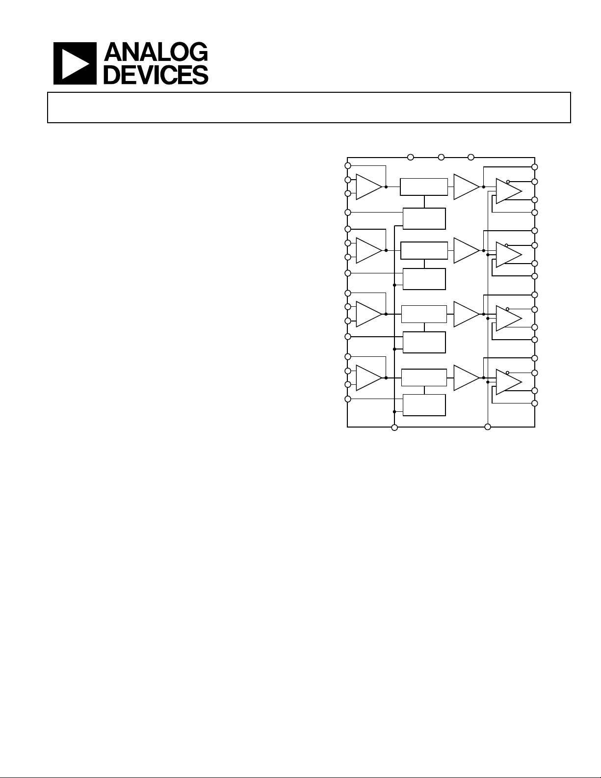
FUNCTIONAL BLOCK DIAGRAM
GENERAL DESCRIPTION
The AD8264 is a 4-channel, linear-in-dB, general-purpose
variable gain amplifier (VGA) with a preamplifier (preamp),
and a flexible differential output buffer. Intended for a broad
range of applications, dc coupling combined with wide bandwidth makes this amplifier a very good pulse processor.
Each channel includes a single-ended input preamp/VGA
section to preserve the wide bandwidth and fast slew rate for lowdistortion pulse applications. A 6 dB differential output buffer
with common-mode and offset adjustments enable direct coupling
to most modern high speed analog-to-digital converters (ADCs),
using the converter reference output for perfect dc matching levels.
The −3 dB bandwidth of the preamp/VGA is dc to 235 MHz,
and the bandwidth of the differential driver is 80 MHz. The
floating gain control interface provides a precise linear-in-dB scale
of 20 dB/V and is easy to interface to a variety of external circuits.
Rev. A
Information furnished by Analog Devices is believed to be accurate and reliable. However, no
responsibility is assumed by Analog Devices for its use, nor for any infringements of patents or other
rights of third parties that may result from its use. Specifications subject to change without notice. No
license is granted by implication or otherwise under any patent or patent rights of Analog Devices.
Trademarks and registered trademarks are the property of their respective owners.
Figure 1.
The gain of each channel is adjusted independently, and all
channels are referenced to a single pin, GNLO. Combined with
a multi-output, digital-to-analog converter (DAC), each section
of the AD8264 can be used for active calibration or as a trim
amplifier.
The gain range of the VGA section is 24 dB. Operation from
a dual polarity power supply enables amplification of negative
voltage pulses that are generated by current-sinking pulses into
a grounded load, such as is typical of photodiodes or photomultiplier tubes (PMT). Delay-free processing of wide-band
video signals is also possible. The differential output amplifier
permits convenient level shifting and interfacing to singlesupply ADCs using the VOCM and OFSx pins.
The AD8264 is available in a 40-lead, 6 mm × 6 mm LFCSP
with an operating temperature range of −40°C to +105°C.
One Technology Way, P.O. Box 9106, Norwood, MA 02062-9106, U.S.A.
Tel: 781.329.4700
Fax: 781.461.3113 ©2009–2011 Analog Devices, Inc. All rights reserved.
www.analog.com
 Loading...