Analog Devices AD826 Datasheet

High-Speed, Low-Power
10
90
100
0%
500ns
5V
5V
CL = 100pF
C
L
= 1000pF
a
FEATURES
High Speed:
50 MHz Unity Gain Bandwidth
350 V/s Slew Rate
70 ns Settling Time to 0.01%
Low Power:
7.5 mA Max Power Supply Current Per Amp
Easy to Use:
Drives Unlimited Capacitive Loads
50 mA Min Output Current Per Amplifier
Specified for +5 V, 5 V and 15 V Operation
2.0 V p-p Output Swing into a 150 Load
= +5 V)
(V
S
Good Video Performance
Differential Gain & Phase Error of 0.07% & 0.11
Excellent DC Performance:
2.0 mV Max Input Offset Voltage
APPLICATIONS
Unity Gain ADC/DAC Buffer
Cable Drivers
8- and 10-Bit Data Acquisition Systems
Video Line Driver
Active Filters
PRODUCT DESCRIPTION
The AD826 is a dual, high speed voltage feedback op amp. It
is ideal for use in applications which require unity gain stability
and high output drive capability, such as buffering and cable
driving. The 50 MHz bandwidth and 350 V/µs slew rate make
the AD826 useful in many high speed applications including:
video, CATV, copiers, LCDs, image scanners and fax machines.
Dual Operational Amplifier
AD826
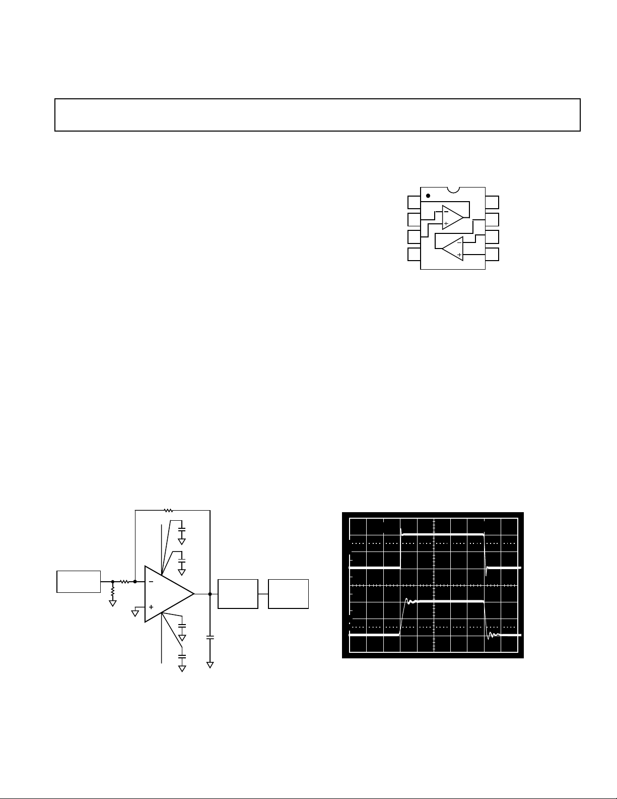
CONNECTION DIAGRAM
8-Lead Plastic Mini-DIP and SO Package
1
OUT1
2
–IN1
+IN1
3
V–
4
AD826
The AD826 features high output current drive capability of
50 mA min per amp, and is able to drive unlimited capacitive
loads. With a low power supply current of 15 mA max for both
amplifiers, the AD826 is a true general purpose operational
amplifier.
The AD826 is ideal for power sensitive applications such as video
cameras and portable instrumentation. The AD826 can operate
from a single +5 V supply, while still achieving 25 MHz of bandwidth. Furthermore the AD826 is fully specified from a single
+5 V to ±15 V power supplies.
The AD826 excels as an ADC/DAC buffer or active filter in
data acquisition systems and achieves a settling time of 70 ns
to 0.01%, with a low input offset voltage of 2 mV max. The
AD826 is available in small 8-lead plastic mini-DIP and SO
packages.
8
V+
7
OUT2
–IN2
6
+IN2
5
1k
V
S
3.3F
0.01F
V
IN
1k
50
2
3
1/2
AD826
–V
S
1
V
OUT
0.01F
3.3F
TEKTRONIX
P6201 FET
PROBE
C
L
TEKTRONIX
7A24 FET
PREAMP
Driving a Large Capacitive Load
HP PULSE
GENERATOR
REV. B
Information furnished by Analog Devices is believed to be accurate and
reliable. However, no responsibility is assumed by Analog Devices for its
use, nor for any infringements of patents or other rights of third parties
which may result from its use. No license is granted by implication or
otherwise under any patent or patent rights of Analog Devices.
One Technology Way, P.O. Box 9106, Norwood, MA 02062-9106, U.S.A.
Tel: 781/329-4700 World Wide Web Site: http://www.analog.com
Fax: 781/326-8703 © Analog Devices, Inc., 2000

AD826–SPECIFICATIONS
(@ TA = +25C, unless otherwise noted)
Parameter Conditions V
S
Min Typ Max Unit
DYNAMIC PERFORMANCE
Unity Gain Bandwidth ±5 V 30 35 MHz
±15 V 45 50 MHz
0, +5 V 25 29 MHz
Bandwidth for 0.1 dB Flatness Gain = +1 ±5 V 10 20 MHz
±15 V 25 55 MHz
Full Power Bandwidth
1
Slew Rate R
V
= 5 V p-p
OUT
= 500 Ω±5 V 15.9 MHz
R
LOAD
V
= 20 V p-p
OUT
R
= 1 kΩ±15 V 5.6 MHz
LOAD
= 1 kΩ±5 V 200 250 V/µs
LOAD
0, +5 V 10 20 MHz
Gain = –1 ±15 V 300 350 V/µs
0, +5 V 150 200 V/µs
Settling Time to 0.1% –2.5 V to +2.5 V ±5 V 45 ns
0 V–10 V Step, A
= –1 ±15 V 45 ns
V
to 0.01% –2.5 V to +2.5 V ±5 V 70 ns
0 V–10 V Step, AV = –1 ±15 V 70 ns
NOISE/HARMONIC PERFORMANCE
Total Harmonic Distortion FC = 1 MHz ±15 V –78 dB
Input Voltage Noise f = 10 kHz ±5 V, ± 15 V 15 nV/√Hz
Input Current Noise f = 10 kHz ±5 V, ± 15 V 1.5 pA/√Hz
Differential Gain Error NTSC ±15 V 0.07 0.1 %
(R1 = 150 Ω) Gain = +2 ±5 V 0.12 0.15 %
0, +5 V 0.15 %
Differential Phase Error NTSC ±15 V 0.11 0.15 Degrees
(R1 = 150 Ω) Gain = +2 ±5 V 0.12 0.15 Degrees
0, +5 V 0.15 Degrees
DC PERFORMANCE
Input Offset Voltage ±5 V to ±15 V 0.5 2 mV
T
MIN
to T
MAX
3mV
Offset Drift 10 µV/°C
Input Bias Current ±5 V, ± 15 V 3.3 6.6 µA
T
T
MIN
MAX
10 µA
4.4 µA
Input Offset Current ±5 V, ± 15 V 25 300 nA
T
MIN
to T
MAX
500 nA
Offset Current Drift 0.3 nA/°C
Open-Loop Gain V
= ±2.5 V ±5 V
OUT
R
= 500 Ω 2 4 V/mV
LOAD
T
to T
R
V
R
T
V
R
MIN
LOAD
OUT
LOAD
MIN
OUT
LOAD
MAX
= 150 Ω 1.5 3 V/mV
= ±10 V ±15 V
= 1 kΩ 3.5 6 V/mV
to T
MAX
= ±7.5 V ±15 V
= 150 Ω (50 mA Output) 2 4 V/mV
1.5 V/mV
2 5 V/mV
INPUT CHARACTERISTICS
Input Resistance 300 kΩ
Input Capacitance 1.5 pF
Input Common-Mode Voltage Range ± 5 V +3.8 +4.3 V
–2.7 –3.4 V
±15 V +13 +14.3 V
–12 –13.4 V
0, +5 V +3.8 +4.3 V
+1.2 +0.9 V
Common-Mode Rejection Ratio V
= ±2.5 V, T
CM
V
= ±12 V ±15 V 86 120 dB
CM
T
to T
MIN
MIN–TMAX
MAX
±5 V 80 100 dB
±15 V 80 100 dB
–2–
REV. B

AD826
2.0
0
–50 90
1.5
0.5
–30
1.0
50 703010–10
80–40 40 60200–20
AMBIENT TEMPERATURE – C
MAXIMUM POWER DISSIPATION – Watts
8-LEAD MINI-DIP PACKAGE
8-LEAD SOIC PACKAGE
TJ = +150C
Parameter Conditions V
OUTPUT CHARACTERISTICS
Output Voltage Swing R
Output Current ±15 V 50 mA
Short-Circuit Current ± 15 V 90 mA
Output Resistance Open Loop 8 Ω
MATCHING CHARACTERISTICS
Dynamic
Crosstalk f = 5 MHz ±15 V –80 dB
Gain Flatness Match G = +1, f = 40 MHz ±15 V 0.2 dB
Slew Rate Match G = –1 ±15 V 10 V/µs
DC
Input Offset Voltage Match T
Input Bias Current Match T
Open-Loop Gain Match V
Common-Mode Rejection Ratio Match V
Power Supply Rejection Ratio Match ± 5 V to ±15 V, T
POWER SUPPLY
Operating Range Dual Supply ±2.5 ± 18 V
Quiescent Current/Amplifier ±5 V 6.6 7.5 mA
Power Supply Rejection Ratio VS = ±5 V to ±15 V, T
NOTES
1
Full power bandwidth = slew rate/2 π V
Specifications subject to change without notice.
ABSOLUTE MAXIMUM RATINGS
Supply Voltage . . . . . . . . . . . . . . . . . . . . . . . . . . . . . . . ±18 V
Internal Power Dissipation
2
Plastic (N) . . . . . . . . . . . . . . . . . . . . . See Derating Curves
Small Outline (R) . . . . . . . . . . . . . . . . See Derating Curves
Input Voltage (Common Mode) . . . . . . . . . . . . . . . . . . . ±V
Differential Input Voltage . . . . . . . . . . . . . . . . . . . . . . . ±6 V
Output Short Circuit Duration . . . . . . . See Derating Curves
Storage Temperature Range (N, R) . . . . . . . –65°C to +125°C
Operating Temperature Range . . . . . . . . . . –40°C to +85°C
Lead Temperature Range (Soldering 10 seconds) . . . +300°C
NOTES
1
Stresses above those listed under Absolute Maximum Ratings may cause perma-
nent damage to the device. This is a stress rating only; functional operation of the
device at these or any other conditions above those indicated in the operational
section of this specification is not implied. Exposure to absolute maximum rating
conditions for extended periods may affect device reliability .
2
Specification is for device in free air: 8-lead plastic package, θJA = 100°C/watt;
8-lead SOIC package, θJA = 155°C/watt.
ORDERING GUIDE
Model Range Description Option
Temperature Package Package
AD826AN – 40°C to +85°C 8-Lead Plastic DIP N-8
AD826AR –40°C to +85°C 8-Lead Plastic SOIC SO-8
AD826AR-REEL7 –40°C to +85°C 7” Tape & Reel SOIC SO-8
AD826AR-REEL –40°C to +85°C 13” Tape & Reel SOIC SO-8
REV. B
PEAK
S
= 500 Ω±5 V 3.3 3.8 ±V
LOAD
= 150 Ω±5 V 3.2 3.6 ±V
R
LOAD
= 1 kΩ±15 V 13.3 13.7 ±V
R
LOAD
= 500 Ω±15 V 12.8 13.4 ±V
R
LOAD
= 500 Ω 0, +5 V +1.5,
R
LOAD
Min Typ Max Unit
+3.5 V
±5 V 50 mA
0, +5 V 30 mA
MIN–TMAX
MIN–TMAX
= ±10 V, R
O
T
MIN–TMAX
= ±12 V, T
CM
= 1 kΩ,
LOAD
MIN–TMAX
MIN–TMAX
±5 V to ±15 V 0.5 2 mV
±5 V to ±15 V 0.06 0.8 µA
±15 V 0.15 0.01 mV/V
±15 V 80 100 dB
80 100 dB
Single Supply +5 +36 V
T
MIN
to T
MAX
±5 V 7.5 mA
±15 V 7.5 mA
T
to T
MIN
.
MAX
to T
MIN
ESD SUSCEPTIBILITY
±15 V 6.8 7.5 mA
MAX
75 86 dB
ESD (electrostatic discharge) sensitive device. Electrostatic charges
1
as high as 4000 volts, which readily accumulate on the human
body and on test equipment, can discharge without detection.
Although the AD826 features proprietary ESD protection circuitry, permanent damage may still occur on these devices
if they are subjected to high energy electrostatic discharges.
Therefore, proper ESD precautions are recommended to avoid
any performance degradation or loss of functionality.
S
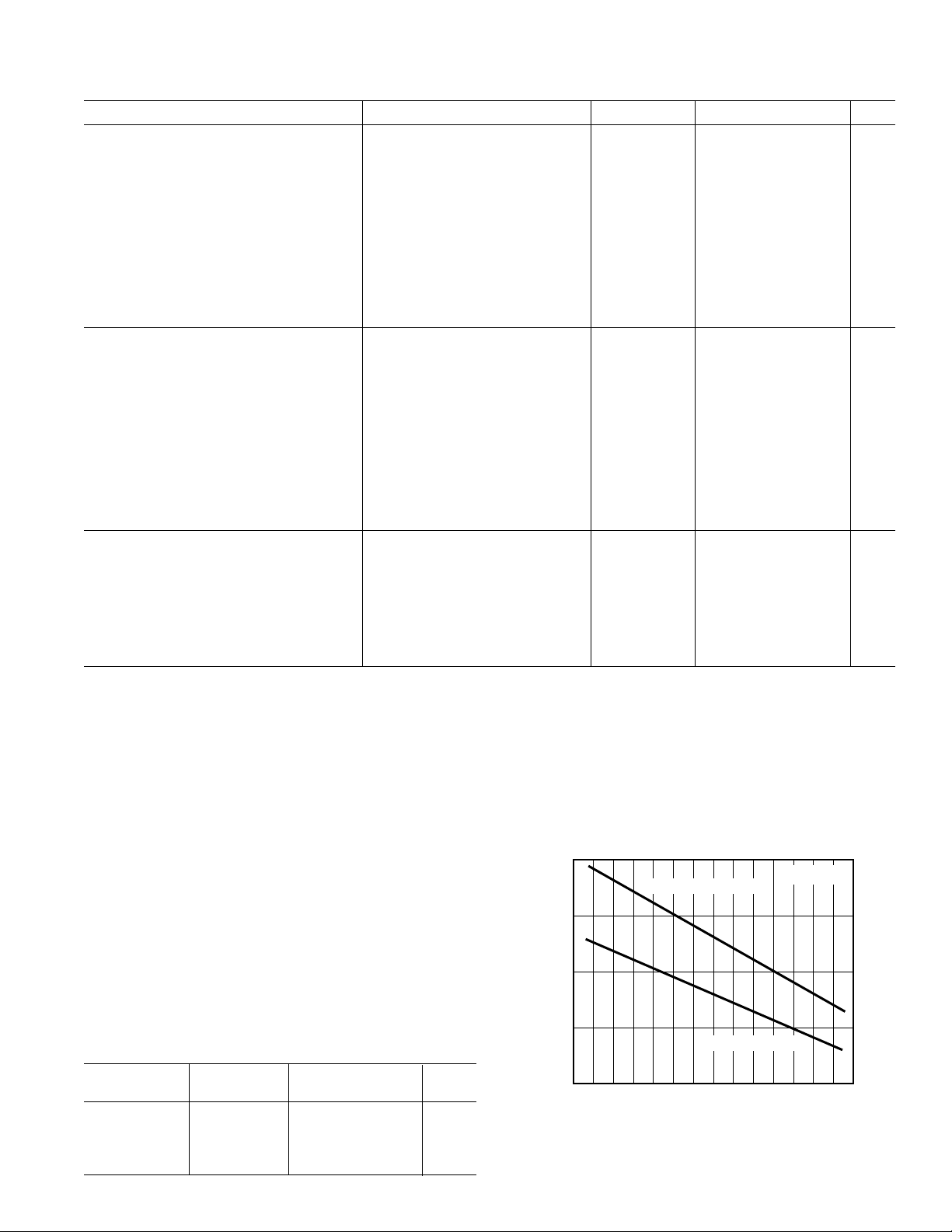
Maximum Power Dissipation vs. Temperature for Different
Package Types
–3–

AD826
– Typical Characteristics
20
15
+V
CM
10
–V
CM
5
INPUT COMMON-MODE RANGE – Volts
0
020
5
SUPPLY VOLTAGE – Volts
10
15
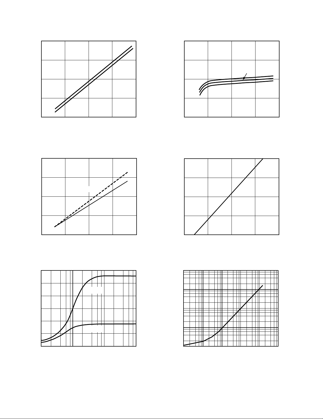
Figure 1. Common-Mode Voltage Range vs. Supply
7.7
7.2
6.7
6.2
QUIESCENT SUPPLY CURRENT PER AMP – mA
5.7
020
Figure 4. Quiescent Supply Current per Amp vs. Supply
Voltage for Various Temperatures
20
15
RL = 500V
10
RL = 150V
5
OUTPUT VOLTAGE SWING – Volts
400
350
300
SLEW RATE – V/s
250
–40C
5
SUPPLY VOLTAGE – Volts
10
+85
C
+25C
15
0
020
5
SUPPLY VOLTAGE – Volts
10
15
Figure 2. Output Voltage Swing vs. Supply
30
25
VS = 15V
20
15
10
5
OUTPUT VOLTAGE SWING – Volts p-p
0
10
100
LOAD RESISTANCE –
VS = 5V
1k
10k
Figure 3. Output Voltage Swing vs. Load Resistance
200
Figure 5. Slew Rate vs. Supply Voltage
100
10
1
0.1
CLOSED-LOOP OUTPUT IMPEDANCE –
0.01
1k 10k 100M10M1M100k
Figure 6. Closed-Loop Output Impedance vs. Frequency
SUPPLY VOLTAGE – Volts
20501510
FREQUENCY – Hz
–4–
REV. B

AD826
7
6
5
4
3
INPUT BIAS CURRENT – A
2
1
–40
–60
TEMPERATURE – C
120806040 100200–20
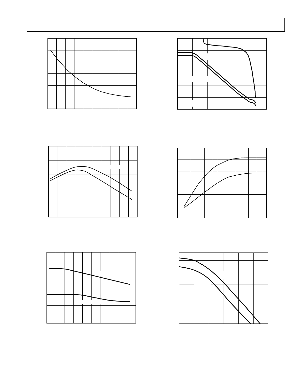
Figure 7. Input Bias Current vs. Temperature
130
110
SOURCE CURRENT
90
SINK CURRENT
70
50
SHORT CIRCUIT CURRENT – mA
140
OPEN-LOOP GAIN – dB
100
–20
80
GAIN 15V SUPPLIES
60
40
20
0
RL = 1k
1k
GAIN 5V SUPPLIES
10k
FREQUENCY – Hz
PHASE 5V OR
15V SUPPLIES
100M10M1M100k
1G
Figure 10. Open-Loop Gain and Phase Margin
vs. Frequency
7
6
5
4
3
OPEN-LOOP GAIN – V/mV
2
15V
5V
+100
+80
+60
+40
+20
0
PHASE MARGIN – Degrees
30
–40
–60
TEMPERATURE – C
140
120100806040200–20
Figure 8. Short Circuit Current vs. Temperature
100
80
60
PHASE MARGIN – Degrees
40
20
–60 140
–40
GAIN BANDWIDTH
TEMPERATURE – C
PHASE MARGIN
100 120806040200–20
80
60
40
20
Figure 9. Unity Gain Bandwidth and Phase Margin
vs. Temperature
UNITY GAIN BANDWIDTH – MHz
1
100 1k 10k
LOAD RESISTANCE –
Figure 11. Open-Loop Gain vs. Load Resistance
100
90
PSR – dB
80
70
60
50
40
30
20
10
NEGATIVE
SUPPLY
1k100
POSITIVE
SUPPLY
FREQUENCY – Hz
100M
10M1M100k10k
Figure 12. Power Supply Rejection vs. Frequency
REV. B
–5–
 Loading...