

Page 1
现货库存、技术资料、百科信息、热点资讯,精彩尽在鼎好!
10 MHz, 20 V/μs, G = 1, 10, 100, 1000 i CMOS®
Programmable Gain Instrumentation Amplifier
Preliminary Technical Data
FEATURES
Small package: 10-lead MSOP
Programmable gains: 1, 10, 100, 1000
Digital or pin-programmable gain setting
Wide supply: ±5 V to ±15 V
Excellent dc performance
High CMRR 120 dB , G = 100
Low gain drift: 10 ppm/°C
Low offset drift: 1.2 V/°C , G = 1000
Excellent ac performance
Fast settling time: 615 ns to 0.001%
High slew rate: 20 V/µs
Low distortion:
High CMRR over frequency: 80 dB to 50 kHz
Low noise: 8 nV/√Hz, G = 1000
Low power: 4 mA
APPLICATIONS
Data acquisition
Biomedical analysis
Test and measurement
GENERAL DESCRIPTION
The AD8253 is an instrumentation amplifier with digitally
programmable gains that has GΩ input impedance, low output
noise, and low distortion making it suitable for interfacing with
sensors and driving high sample rate analog-to-digital converters
(ADCs). It has high bandwidth of 10 MHz, low THD and fast
settling time of 615 ns to 0.001%. Offset drift and gain drift are
specified to 1.2 μV/°C and 10 ppm/°C, respectively for G = 1000.
In addition to its wide input common voltage range, it boasts a
high common-mode rejection of 80 dB at G = 1 from dc to
50 kHz. The combination of precision dc performance coupled
with high speed capabilities make the AD8253 an excellent
candidate for data acquisition. Furthermore, this monolithic
solution simplifies design and manufacturing, and boosts
performance of instrumentation by maintaining a tight match
of internal resistors and amplifiers.
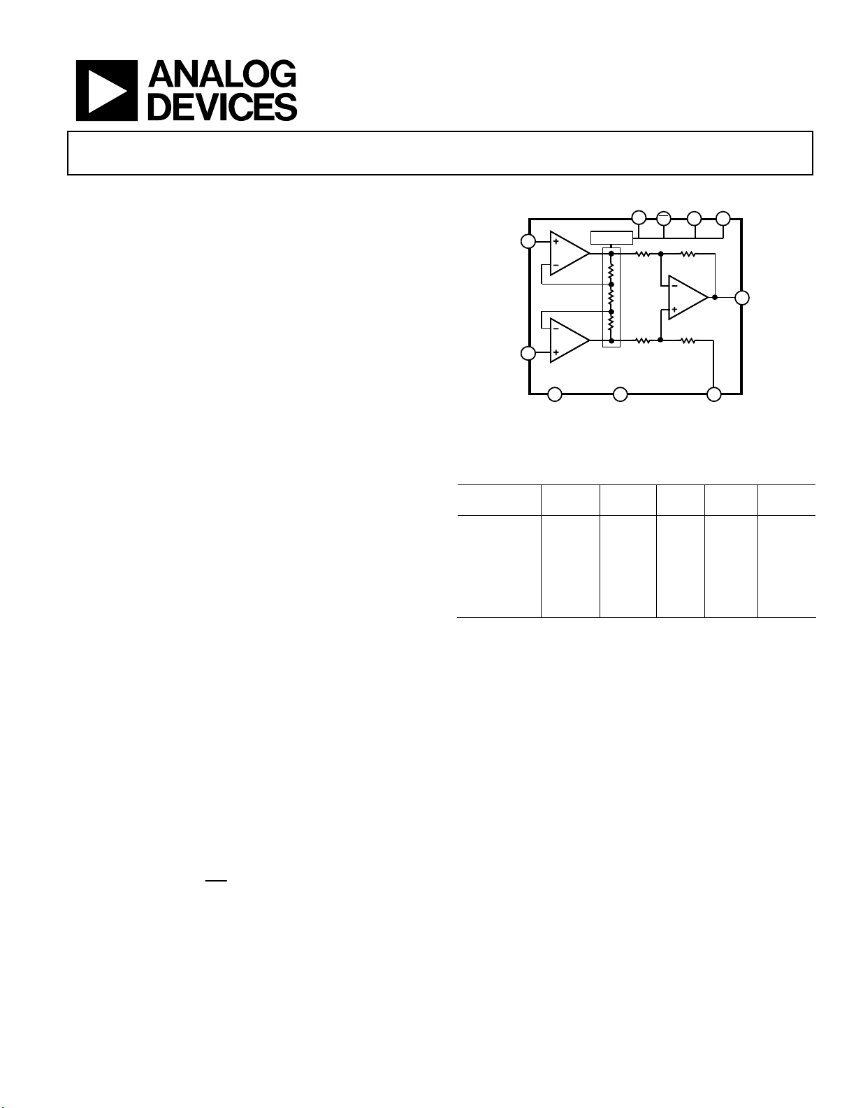
The AD8253 user interface consists of a parallel port that allows
users to set the gain in one of two different ways (see Figure 1
for the functional block diagram). A 2-bit word sent via a bus
WR
can be latched using the
transparent gain mode where the state of logic levels at the gain
port determines the gain.
input. An alternative is to use
AD8253
FUNCTIONAL BLOCK DIAGRAM
DGD
-IN
+IN
+VS -VS REF
Logic
Figure 1.
Table 1. Instrumentation and Difference Amplifiers by
Category
High
Performance
AD82201 AD6231
AD8221
AD8222 AD524 AD8251
AD82241
AD624
1
Rail-to-rail output.
Low
Cost
AD8553
High
Voltage
AD628 AD620
1
AD629 AD621 AD8250
The AD8253 is available in a 10-lead MSOP package and is
specified over the −40°C to +85°C temperature range, making it
an excellent solution for applications where size and packing
density are important considerations.
WR
AD8253
Mil
Grade
AD526
A1 A0
OUT
Low
Power
AD6271 AD82311
Digital
Gain
AD85551
AD8556
AD8557
1
1
Rev. prA
Information furnished by Analog Devices is believed to be accurate and reliable. However, no
responsibility is assumed by Anal og Devices for its use, nor for any infringements of patents or ot her
rights of third parties that may result from its use. Specifications subject to change without notice. No
license is granted by implication or otherwise under any patent or patent rights of Analog Devices.
Trademarks and registered trademarks are the property of their respective owners.
One Technology Way, P.O. Box 9106, Norwood, MA 02062-9106, U.S.A.
Tel: 781.329.4700 www.analog.com
Fax: 781.461.3113 ©2007 Analog Devices, Inc. All rights reserved.
Page 2

AD8253 Preliminary Technical Data
TABLE OF CONTENTS
Features.............................................................................................. 1
Applications....................................................................................... 1
General Description ......................................................................... 1
Functional Block Diagram .............................................................. 1
Revision History ............................................................................... 2
Specifications..................................................................................... 3
Timing Diagram........................................................................... 5
Absolute Maximum Ratings............................................................ 6
REVISION HISTORY
4/07—Revision 0: Initial Version
Maximum Power Dissipation......................................................6
ESD Caution...................................................................................6
Pin Configuration and Function Descriptions..............................7
Theory of Operation .........................................................................8
Gain Selection................................................................................8
Outline Dimensions....................................................................... 10
Ordering Guide .......................................................................... 10
Rev. prA | Page 2 of 10
Page 3

Preliminary Technical Data AD8253
SPECIFICATIONS
+VS = +15 V, −VS = −15 V, V
Table 2.
Parameter Conditions Min Typ Max Unit
COMMON-MODE REJECTION RATIO (CMRR)
CMRR to 60 Hz with 1 kΩ Source Imbalance +IN = −IN = −10 V to +10 V
G = 1 80 dB
G = 10 100 dB
G = 100 120 dB
G = 1000 120 dB
CMRR to 50 kHz +IN = −IN = −10 V to +10 V
G = 1 80 dB
G = 10 dB
G = 100 dB
G = 1000 dB
NOISE
Voltage Noise, 1 kHz, RTI
G = 1 40 nV/√Hz
G = 10 9 nV/√Hz
G = 100 8 nV/√Hz
G = 1000 8 nV/√Hz
0.1 Hz to 10 Hz, RTI
G = 1 2.5 μV p-p
G = 10 2.5 μV p-p
G = 100 μV p-p
G = 1000 μV p-p
Current Noise, 1 kHz 5 pA/√Hz
Current Noise, 0.1 Hz to 10 Hz 60 pA p-p
VOLTAGE OFFSET
Offset RTI VOS G = 1, 10, 100, 1000 ±200 + 600/G μV
Over Temperature T = −40°C to +85°C ±260 + 900/G μV
Average TC T = −40°C to +85°C ±1.2 + 5/G μV/°C
Offset Referred to the Input vs. Supply (PSR) VS = ±5 V to ±15 V ±6 + 20/G μV/V
INPUT CURRENT
Input Bias Current 5 30 nA
Over Temperature T = −40°C to +85°C 40 nA
Average TC 400 pA/°C
Input Offset Current 5 30 nA
Over Temperature T = −40°C to +85°C 30 nA
Average TC 160 pA/°C
DYNAMIC RESPONSE
Small Signal −3 dB Bandwidth
G = 1 10 MHz
G = 10 6 MHz
G = 100 3 MHz
G = 1000 0.3 MHz
Settling Time 0.01% ΔOUT = 10 V step
G = 1 585 ns
G = 10 648 ns
G = 100 ns
G = 1000 ns
= 0 V @ TA = 25°C, G = 1, RL = 2 kΩ, unless otherwise noted.
REF
Rev. prA | Page 3 of 10
Page 4

AD8253 Preliminary Technical Data
Parameter Conditions Min Typ Max Unit
Settling Time 0.001% ΔOUT = 10 V step
G = 1 615 ns
G = 10 685 ns
G = 100 ns
G = 1000 ns
Slew Rate
G = 1 20 V/μs
G = 10 25 V/μs
G = 100 25 V/μs
G = 1000 25 V/μs
Total Harmonic Distortion f = 1 kHz, RL = 10 kΩ, G = 1 dB
GAIN
Gain Range G = 1, 10, 100, 1000 1 1000 V/V
Gain Error OUT = ±10 V
G = 1 0.03 %
G = 10 0.04 %
G = 100 %
G = 1000 %
Gain Nonlinearity OUT = −10 V to +10 V
G = 1 RL = 10 kΩ, 2 kΩ, 600 Ω 6 ppm
G = 10 RL = 10 kΩ, 2 kΩ, 600 Ω 10 ppm
G = 100 RL = 10 kΩ, 2 kΩ, 600 Ω ppm
G = 1000 RL = 10 kΩ, 2 kΩ, 600 Ω ppm
Gain vs. Temperature All gains 10 ppm/°C
INPUT
Input Impedance
Differential 1
Common Mode 1
Input Operating Voltage Range VS = ±5 V to ±15 V −VS + 1.0 +VS − 1.1 V
Over Temperature T = −40°C to +85°C −VS + 1.1 +VS − 1.4 V
OUTPUT
Output Swing −13.5 +13.5 V
Over Temperature T = −40°C to +85°C −13.5 +13.5 V
Short-Circuit Current 37 mA
REFERENCE INPUT
RIN 20 kΩ
IIN +IN, −IN, REF = 0 1 μA
Voltage Range −VS +VS V
Gain to Output
1 ± 0.0001
V/V
DIGITAL LOGIC
Digital Ground Voltage, DGND Referred to GND −VS + 4.25 0 +VS − 2.7 V
Digital Input Voltage Low Referred to GND DGND 2.1 V
Digital Input Voltage High Referred to GND 2.8 +VS V
Digital Input Current 1 μA
Gain Switching Time1 325 ns
t
See Figure 2 timing diagram 20 ns
SU
tHD 10 ns
t
-LOW
WR
t
-HIGH
WR
20 ns
40 ns
GΩ||pF
GΩ||pF
Rev. prA | Page 4 of 10
Page 5

Preliminary Technical Data AD8253
Parameter Conditions Min Typ Max Unit
POWER SUPPLY
Operating Range ±5 ±15 V
Quiescent Current, +IS 4.1 4.5 mA
Quiescent Current, −IS 3.7 4.5 mA
Over Temperature T = −40°C to +85°C 4.5 mA
TEMPERATURE RANGE
Specified Performance −40 +85 °C
1
Add time for the output to slew and settle to calculate the total time for a gain change.
TIMING DIAGRAM
WR
t
WR-HIGH
t
WR-LOW
A0, A1
t
SU
t
HD
6287-003
Figure 2. Timing Diagram for Latched Gain Mode (See the Timing for Latched Gain Mode Section)
Rev. prA | Page 5 of 10
Page 6

AD8253 Preliminary Technical Data
(
)
ABSOLUTE MAXIMUM RATINGS
Table 3.
Parameter Rating
Supply Voltage ±17 V
Power Dissipation See Figure 3
Output Short-Circuit Current Indefinite1
Common-Mode Input Voltage ±VS
Differential Input Voltage ±VS
Digital Logic Inputs ±VS
Storage Temperature Range –65°C to +125°C
Operating Temperature Range2 –40°C to +85°C
Lead Temperature (Soldering 10 sec) 300°C
Junction Temperature 140°C
θJA (4-Layer JEDEC Standard Board) 112°C/W
Package Glass Transition Temperature 140°C
1
Assumes the load is referenced to mid supply.
2
Temperature for specified performance is −40°C to +85°C. For performance
to +125°C, see the Error! Reference source not found. section.
Stresses above those listed under Absolute Maximum Ratings
may cause permanent damage to the device. This is a stress
rating only; functional operation of the device at these or any
other conditions above those indicated in the operational
section of this specification is not implied. Exposure to absolute
maximum rating conditions for extended periods may affect
device reliability.
MAXIMUM POWER DISSIPATION
The maximum safe power dissipation in the AD8253 package is
limited by the associated rise in junction temperature (T
the die. The plastic encapsulating the die locally reaches the
junction temperature. At approximately 140°C, which is the
glass transition temperature, the plastic changes its properties.
Even temporarily exceeding this temperature limit may change
the stresses that the package exerts on the die, permanently
shifting the parametric performance of the AD8253. Exceeding
a junction temperature of 140°C for an extended period can
result in changes in silicon devices, potentially causing failure.
The still-air thermal properties of the package and PCB (θ
the ambient temperature (T
the package (P
) determine the junction temperature of the die.
D
), and the total power dissipated in
A
The junction temperature is calculated as
PTT θ×+=
J
The power dissipated in the package (P
D
A
JA
) is the sum of the
D
quiescent power dissipation and the power dissipated in the
) on
J
JA
),
package due to the load drive for all outputs. The quiescent
power is the voltage between the supply pins (V
quiescent current (I
midsupply, the total drive power is V
). Assuming the load (RL) is referenced to
S
/2 × I
S
dissipated in the package and some in the load (V
) times the
S
, some of which is
OUT
× I
OUT
OUT
).
The difference between the total drive power and the load
power is the drive power dissipated in the package.
P
= Quiescent Power + (Total Drive Power − Load Power)
D
⎛
()
D
⎜
IVP
SS
⎜
⎝
V
2
⎞
V
OUTS
⎟
×+×=
⎟
R
L
⎠
In single-supply operation with R
= VS/2.
is V
OUT
Airflow increases heat dissipation, effectively reducing θ
2
V
OUT
–
R
L
referenced to −VS, worst case
L
. In
JA
addition, more metal directly in contact with the package leads
from metal traces, through holes, ground, and power planes
reduces the θ
.
JA
Figure 3 shows the maximum safe power dissipation in the
package vs. the ambient temperature on a 4-layer JEDEC
standard board.
2.00
1.75
1.50
1.25
1.00
0.75
0.50
MAXIMUM POWER DISSIPATI ON (W)
0.25
0
–40 –20 120100806040200
Figure 3. Maximum Power Dissipation vs. Ambient Temperature
AMBIENT TEMPERATURE (°C)
06287-004
ESD CAUTION
Rev. prA | Page 6 of 10
Page 7

Preliminary Technical Data AD8253
PIN CONFIGURATION AND FUNCTION
DESCRIPTIONS
1
-IN
2
DGND
-VS
A0
A1
Figure 4. 10-Lead MSOP (RM-10) Pin Configuration
AD8253
3
TOP VIEW
(Not to Scale)
4
5
NC = NO CONNECT
Table 4. Pin Function Descriptions
Pin No. Name Description
1 −IN
Inverting Input Terminal. True
10
9
8
7
6
+IN
VREF
+VS
VOUT
WR
2 DGND Digital Ground.
3 −VS Negative Supply Terminal.
4 A0 Gain Setting Pin (LSB).
5 A1 Gain Setting Pin (MSB).
6
WR
7 OUT Output Terminal.
8 +VS Positive Supply Terminal.
9 REF Reference Voltage Terminal.
10 +IN
differential input.
Write Enable.
Noninverting Input Terminal. True
differential input.
Rev. prA | Page 7 of 10
Page 8
AD8253 Preliminary Technical Data
–
V
V
THEORY OF OPERATION
+IN
+
S
+V
S
2.2kΩ
IN
–V
S
+V
S
2.2kΩ
–V
S
–V
A1
DIGITAL
GAIN
CONTROL
A2
+V
WR
S
S
2.2kΩ
2.2kΩ
+
S
A1A0
–V
S
10kΩ 10kΩ
10kΩ
+V
S
DGND
A3
10kΩ
+V
S
OUTPUT
–V
S
+V
S
REF
–V
S
–V
S
Figure 5. Simplified Schematic
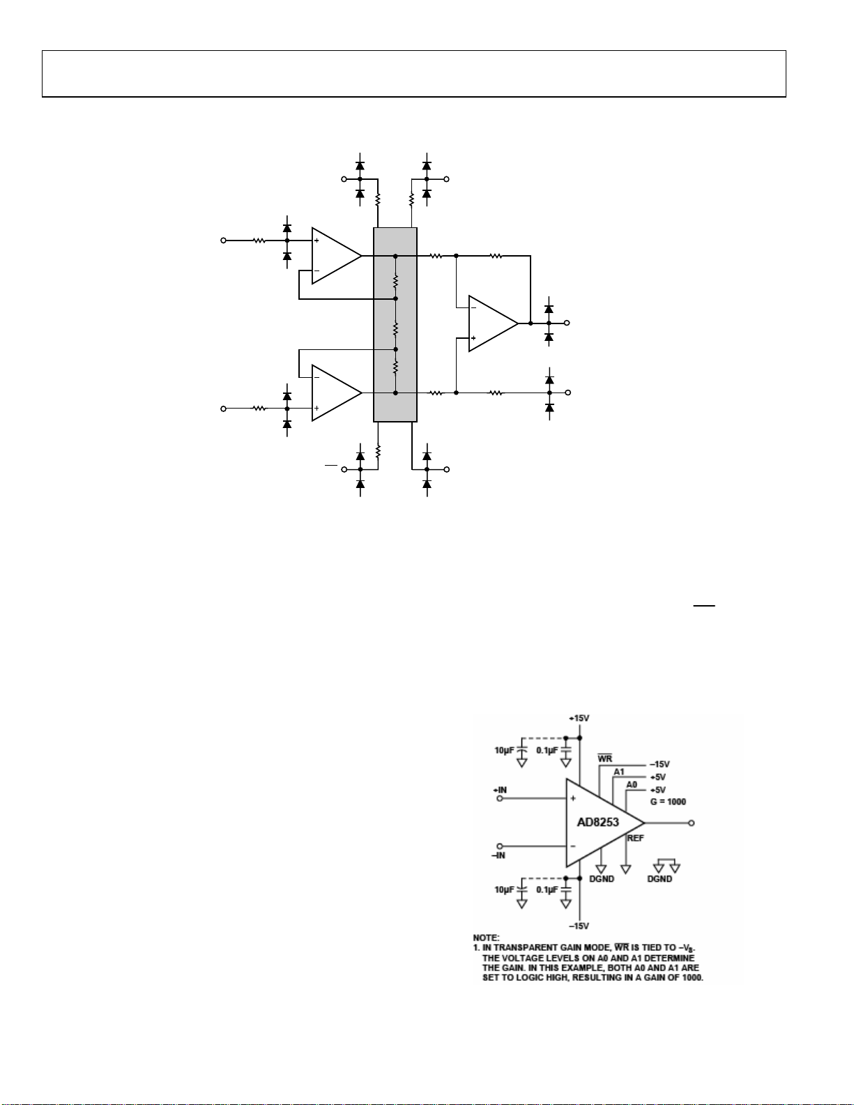
The AD8253 is a monolithic instrumentation amplifier based
on the classic, three op amp topology as shown in Figure 5.
It is fabricated on the Analog Devices, Inc. proprietary iCMOS
process that provides precision, linear performance ,and a robust
digital interface. A parallel interface allows users to digitally
program gains of 1, 10, 100, and 1000. Gain control is achieved
by switching resistors in an internal, precision, resistor array (as
shown in Figure 5). Although the AD8253 has a voltage feedback topology, gain bandwidth product increases for gains of 1,
10, and 100 because each gain has its own frequency
compensation. This results in maximum bandwidth at higher
gains.
All internal amplifiers employ distortion cancellation circuitry
and achieve high linearity and ultralow THD. Laser trimmed
resistors allow for a maximum gain error of less than 0.03% for
G = 1, and minimum CMRR of 120 dB for G = 1000. A pinout
optimized for high CMRR over frequency enables the AD8253
to offer CMRR over frequency of 80 dB at 50 kHz (G = 1). The
balanced input reduces the parasitics that, in the past, had
adversely affected CMRR performance.
GAIN SELECTION
This section shows users how to configure the AD8253 for basic
operation. Logic low and Logic high voltage limits are listed in
the Specifications section. Typically, logic low is 0 V and
logic high is 5 V; both voltages are measured with respect
to DGND. Refer to the specifications table (Table 2) for
the permissible voltage range of DGND. The gain of the
AD8253 can be set using two methods.
–V
S
6287-050
Transparent Gain Mode
The easiest way to set the gain is to program it directly via a
logic high or logic low voltage applied to A0 and A1. Figure 6
shows an example of this gain setting method, referred to throughout the data sheet as transparent gain mode. Tie
WR
to the
negative supply to engage transparent gain mode. In this mode,
any change in voltage applied to A0 and A1 from logic low to
logic high, or vice versa, immediately results in a gain change.
Table 5 is the truth table for transparent gain mode and Figure 6
shows the AD8253 configured in transparent gain mode.
Figure 6. Transparent Gain Mode, A0 and A1 = High, G = 1000
Rev. prA | Page 8 of 10
Page 9

Preliminary Technical Data AD8253
Table 5. Truth Table Logic Levels for Transparent Gain Mode
A1 A0 Gain
WR
−VS Low Low 1
−VS Low High 10
−VS High Low 100
−VS High High 1000
Latched Gain Mode
Some applications have multiple programmable devices such as
multiplexers or other programmable gain instrumentation
amplifiers on the same PCB. In such cases, devices can share a
data bus. The gain of the AD8253 can be set using
WR
as a latch,
allowing other devices to share A0 and A1. Figure 7 shows a
schematic using this method, known as latched gain mode. The
AD8253 is in this mode when
WR
is held at logic high or logic
low, typically 5 V and 0 V, respectively. The voltages on A0 and
A1 are read on the downward edge of the
WR
signal as it
transitions from logic high to logic low. This latches in the logic
levels on A0 and A1, resulting in a gain change. See the truth
table listing in Table 6 for more on these gain changes.
Figure 7. Latched Gain Mode, G = 1000
Table 6. Truth Table Logic Levels for Latched Gain Mode
A1 A0 Gain
WR
High to Low Low Low Change to 1
High to Low Low High Change to 10
High to Low High Low Change to 100
High to Low High High Change to 1000
Low to Low X1 X
Low to High X1 X
High to High X1 X
1
X = don’t care.
1
No Change
1
No Change
1
No Change
Upon power-up, the AD8253 defaults to a gain of 1 when in
latched gain mode. In contrast, if the AD8253 is configured in
transparent gain mode, it starts at the gain indicated by the
voltage levels on A0 and A1 upon power-up.
Timing for Latched Gain Mode
In latched gain mode, logic levels at A0 and A1 have to be held
for a minimum setup time, t
WR
latches in the gain. Similarly, they must be held for a
minimum hold time of t
ensure that the gain is latched in correctly. After t
, before the downward edge of
SU
after the downward edge of WR to
HD
, A0 and A1
HD
may change logic levels but the gain does not change (until the
WR
next downward edge of
can be held high is t
WR
duration that
can be held low. Digital timing specifications
). The minimum duration that WR
WR-HIGH
, and t
is the minimum
WR-LOW
are listed in Table 2. The time required for a gain change is
dominated by the settling time of the amplifier. A timing
diagram is shown in Figure 8.
When sharing a data bus with other devices, logic levels applied
to those devices can potentially feed through to the output of
the AD8253. Feedthrough can be minimized by decreasing the
edge rate of the logic signals. Furthermore, careful layout of the
PCB also reduces coupling between the digital and analog
portions of the board.
t
WR-HIGH
WR
t
SU
A0, A1
Figure 8. Timing Diagram for Latched Gain Mode
Rev. prA | Page 9 of 10
t
WR-LOW
t
HD
6287-053
Page 10

AD8253 Preliminary Technical Data
OUTLINE DIMENSIONS
3.10
3.00
2.90
6
3.10
3.00
2.90
PIN 1
0.95
0.85
0.75
0.15
0.05
10
1
0.50 BSC
0.33
0.17
COPLANARITY
0.10
5.15
4.90
4.65
5
1.10 MAX
0.80
0.60
0.40
SEATING
PLANE
0.23
0.08
8°
0°
COMPLIANT TO JEDEC STANDARDS MO-187-BA
Figure 9. 10-Lead Mini Small Outline Package [MSOP]
(RM-10)
Dimensions shown in millimeters
ORDERING GUIDE
Model Temperature Range Package Description Package Option Branding
AD8253ARMZ1 –40°C to +85°C 10-Lead MSOP RM-10 Y0K
AD8253ARMZ-RL1 –40°C to +85°C 10-Lead MSOP RM-10 Y0K
AD8253ARMZ-R71 –40°C to +85°C 10-Lead MSOP RM-10 Y0K
AD8253-EVALZ1 Evaluation Board
1
Z = RoHS compliant part.
Rev. PrA | Page 10 of 10 PR06983-0-9/07(PrA)
 Loading...