

Wide Supply Dual, 17 MHz, Rail-to-Rail
Data Sheet
FEATURES
Single-supply operation
Output swings rail-to-rail
Input voltage range extends below ground
Single-supply capability from 3 V to 36 V
High load drive
Capacitive load drive of 470 pF (G = +1, 25% overshoot)
Linear output current of 40 mA, 0.5 V from supplies
Excellent ac performance on 2.6 mA/amplifier
−3 dB bandwidth of 17 MHz, G = +1
325 ns settling time to 0.01% (2 V step)
Slew rate of 30 V/μs
Low distortion: −108 dBc at 20 kHz (G = −1, R
Good dc performance
700 μV maximum input offset voltage
1 μV/°C offset voltage drift
25 pA maximum input bias current
Low noise: 14 nV/√Hz at 10 kHz
No phase inversion with inputs to the supply rails
APPLICATIONS
Photodiode preamps
Active filters
12-bit to 16-bit data acquisition systems
Medical instrumentation
Precision instrumentation
GENERAL DESCRIPTION
The AD823A is a dual precision, 17 MHz, JFET input op amp
manufactured in the extra fast complementary bipolar (XFCB)
process. The AD823A can operate from a single supply of 3 V
to 36 V or from dual supplies of ±1.5 V to ±18 V. It has true
single-supply capability with an input voltage range extending
below ground in single-supply mode. Output voltage swing extends
to within 20 mV of each rail for IOUT ≤ 100 μA, providing
outstanding output dynamic range. It also has a linear output
current of 40 mA, 0.5 V from the supply rails.
An offset voltage of 700 μV maximum, an offset voltage drift of
1 μV/°C, and typical input bias currents of 0.3 pA provide dc
precision with source impedances up to 1 GΩ. The AD823A
provides 17 MHz, −3 dB bandwidth, and a 30 V/μs slew rate with
a low supply current of only 2.6 mA per amplifier. It also provides
low input voltage noise of 14 nV/√Hz and −108 dB SFDR at
20 kHz. The AD823A has low input capacitances (0.6 pF differential and 1.3 pF common mode) and drives more than 500 pF
of direct capacitive load as a follower. This lets the amplifier
handle a wide range of load conditions.
= 2 kΩ)
L
FET Input Amplifier
AD823A
CONNECTION DIAGRAM
1
OUT1
–IN1
2
3
+IN1
–V
4
S
AD823A
Figure 1. 8-Lead SOIC
AD823A
OUT1 1
2
–IN1
+IN1 3
–V
4
S
TOP VIEW
(Not to Scale)
Figure 2. 8-Lead MSOP
VS = 3V
C
= 50pF
L
G = +1
3.0V
1.5V
0V
500mV/DIV
Figure 3. Output Swing, +V
This combination of ac and dc performance, plus the outstanding
load drive capability, results in an exceptionally versatile amplifier for applications such as ADC drivers, high speed active filters,
and other low voltage, high dynamic range systems.
The AD823A is available over the industrial temperature range
of −40°C to +85°C and is offered in an 8-lead SOIC package and
an 8-lead MSOP package.
8
+V
S
OUT2
7
–IN2
6
+IN2
5
09439-001
+V
8
S
7
OUT2
–IN26
+IN25
09439-102
200µs/DIV
= +3 V, G = +1
S
9439-049
Rev. B
Information furnished by Analog Devices is believed to be accurate and reliable. However, no
responsibility is assumed by Analog Devices for its use, nor for any infringements of patents or other
rights of third parties that may result from its use. Specifications subject to change without notice. No
license is granted by implication or otherwise under any patent or patent rights of Analog Devices.
Trademarks and registered trademarks are the property of their respective owners.
One Technology Way, P.O. Box 9106, Norwood, MA 02062-9106, U.S.A.
Tel: 781.329.4700 www.analog.com
Fax: 781.461.3113 ©2012 Analog Devices, Inc. All rights reserved.

AD823A Data Sheet
TABLE OF CONTENTS
Features .............................................................................................. 1
Applications ....................................................................................... 1
General Description ......................................................................... 1
Connection Diagram ....................................................................... 1
Revision History ............................................................................... 2
Specifications ..................................................................................... 3
5 V Operation ............................................................................... 3
3.3 V Operation ............................................................................ 4
±15 V Operation ........................................................................... 5
Absolute Maximum Ratings ............................................................ 6
Thermal Resistance ...................................................................... 6
ESD Caution .................................................................................. 6
REVISION HISTORY
6/12—Rev. A to Rev. B
Added Text to Absolute Maximum Ratings Section .................... 6
Changes to Equation 8 ................................................................... 18
5/12—Revision A: Initial Version
Pin Configuration and Function Descriptions ..............................7
Typical Performance Characteristics ..............................................8
Theory of Operation ...................................................................... 14
Output Impedance ..................................................................... 14
Applications Information .............................................................. 15
Input Characteristics .................................................................. 15
Output Characteristics............................................................... 15
Wideband Photodiode Preamp ................................................ 16
Active Filter ................................................................................. 18
Maximizing Performance Through Proper Layout ............... 19
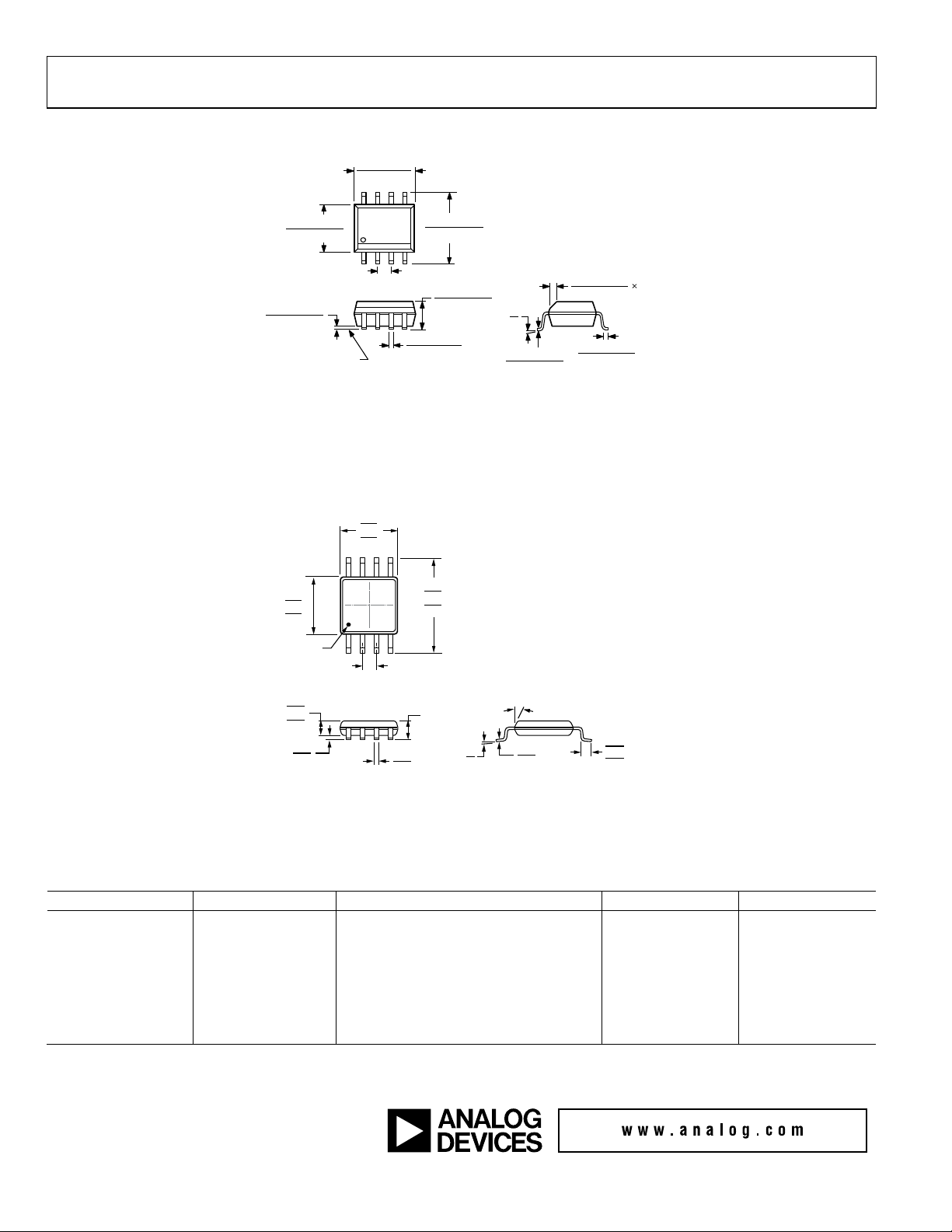
Outline Dimensions ....................................................................... 20
Ordering Guide .......................................................................... 20
Rev. B | Page 2 of 20

Data Sheet AD823A
Slew Rate
G = −1, V
= 4 V step
25
30 V/µs
V
= 2 V p-p, f = 20 kHz, G = +1, RL = 1 kΩ
−99 dBc
Maximum Offset over Temperature
0.2
1.3
mV
Open-Loop Gain
V
= 0.2 V to 4 V, RL = 2 kΩ
40
175 V/mV
IL = ±2 mA
0.026 to 4.96
V
B
SPECIFICATIONS
5 V OPERATION
TA = 25°C, +VS = 5 V, RL = 2 kΩ to 2.5 V, unless otherwise noted.
Table 1.
Parameter Conditions Min Typ Max Unit
DYNAMIC PERFORMANCE
−3 dB Bandwidth G = +1, V
Full Power Response V
OUT
Settling Time
To 0.1% G = −1, V
To 0.01% G = −1, V
NOISE/DISTORTION PERFORMANCE
Input Voltage Noise f = 10 kHz 14 nV/√Hz
Input Current Noise f = 1 kHz 1 fA/√Hz
Harmonic Distortion (SFDR) V
OUT
OUT
Crosstalk
f = 1 kHz RL = 5 kΩ −123 dB
f = 1 MHz RL = 5 kΩ −77 dB
DC PERFORMANCE
Initial Offset 0.12 0.7 mV
≤ 0.2 V p-p 14.1 17 MHz
OUT
= 2 V p-p 4.8 MHz
OUT
= 2 V step 240 ns
OUT
= 2 V step 325 ns
OUT
= 2 V p-p, f = 20 kHz, G = −1, RF = RG = 4 kΩ −108 dBc
Offset Drift 1 µV/°C
Input Bias Current VCM = 0 V to 4 V 0.3 25 pA
At T
VCM = 0 V to 4 V 10 25 pA
MAX
Input Offset Current 0.3 20 pA
At T
3.5 pA
MAX
OUT
T
to T
MIN
25 V/mV
MAX
INPUT CHARACTERISTICS
Input Common-Mode Voltage Range −0.2 to +3 −0.2 to +3.8 V
Input Resistance 1013 Ω
Input Capacitance Differential Mode 0.6 pF
Common Mode 1.3 pF
Common-Mode Rejection Ratio VCM = 0 V to 3 V 60 73 dB
OUTPUT CHARACTERISTICS
Output Voltage Swing
IL = ±100 µA 0.009 to 4.98 V
IL = ±10 mA 0.097 to 4.88 V
Linear Output Current V
= 0.5 V to 4.5 V 40 mA
OUT
Short-Circuit Current Sourcing to 2.5 V 50 mA
Sinking to 2.5 V 101 mA
Capacitive Load Drive G = +1 500 pF
POWER SUPPLY
Operating Range 3 36 V
Quiescent Current T
Power Supply Rejection Ratio VS = 5 V to 15 V, T
MIN
to T
, total 5.1 5.7 mA
MAX
to T
MIN
70 94 dB
MAX
Rev. | Page 3 of 20

AD823A Data Sheet
To 0.1%
G = −1, V
= 2 V step
350 ns
Input Voltage Noise
f = 10 kHz
14 nV/√Hz
f = 1 kHz
RL = 5 kΩ
−123
dB
Initial Offset
0.14 1 mV
At T
3.5 pA
Common Mode
1.3 pF
Output Voltage Swing
B
3.3 V OPERATION
TA = 25°C, +VS = 3.3 V, RL = 2 kΩ to 1.65 V, unless otherwise noted.
Table 2.
Parameter Conditions Min Typ Max Unit
DYNAMIC PERFORMANCE
−3 dB Bandwidth G = +1, V
Full Power Response V
OUT
Slew Rate G = −1, V
Settling Time
To 0.01% G = −1, V
NOISE/DISTORTION PERFORMANCE
Input Current Noise f = 1 kHz 1 fA/√Hz
Harmonic Distortion (SFDR) V
V
OUT
OUT
Crosstalk
f = 1 MHz RL = 5 kΩ −77 dB
DC PERFORMANCE
≤ 0.2 V p-p, VCM = 0.65 V 13.8 17.3 MHz
OUT
= 2 V p-p 3.7 MHz
= 2 V step, VCM = 0.65 V 18 23 V/µs
OUT
OUT
= 2 V step 460 ns
OUT
= 2 V p-p, f = 20 kHz, G = −1, RF = RG = 4 kΩ −108 dBc
= 2 V p-p, f = 20 kHz, G = +1, RL = 100 Ω −70 dBc
Maximum Offset over Temperature 0.3 1.8 mV
Offset Drift 1 µV/°C
Input Bias Current VCM = 0 V to 2 V 0.3 25 pA
At T
VCM = 0 V to 2 V 10 25 pA
MAX
Input Offset Current 0.3 20 pA
MAX
Open-Loop Gain V
T
to T
MIN
14 V/mV
MAX
= 0.2 V to 2 V, RL = 2 kΩ 16 63 V/mV
OUT
INPUT CHARACTERISTICS
Input Common-Mode Voltage Range
−0.2 to
−0.2 to +1.8 V
+1
Input Resistance 1013 Ω
Input Capacitance Differential Mode 0.6 pF
Common-Mode Rejection Ratio VCM = 0 V to 1 V 54 71 dB
OUTPUT CHARACTERISTICS
IL = ±100 µA 0.006 to 3.28 V
IL = ±2 mA 0.04 to 3.26 V
IL = ±10 mA 0.093 to 3.18 V
Linear Output Current V
= 0.5 V to 2.5 V 40 mA
OUT
Short-Circuit Current Sourcing to 1.5 V 44 mA
Sinking to 1.5 V 86 mA
Capacitive Load Drive G = +1 500 pF
POWER SUPPLY
Operating Range 3 36 V
Quiescent Current T
Power Supply Rejection Ratio VS = 3.3 V to 15 V, T
MIN
to T
, total 5.0 5.7 mA
MAX
to T
MIN
70 80 dB
MAX
Rev. | Page 4 of 20

Data Sheet AD823A
To 0.1%
G = −1, V
= 10 V step
380 ns
Input Voltage Noise
f = 10 kHz
13 nV/√Hz
DC PERFORMANCE
At T
VCM = 0 V
55
95
pA
Common-Mode Rejection Ratio
VCM = −15 V to +13 V
70
90 dB
IL = ±100 µA
−14.9 to +14.96
V
Linear Output Current
V
= −14.5 V to +14.5 V
44 mA
B
±15 V OPERATION
TA = 25°C, VS = ±15 V, RL = 2 kΩ to 0 V, unless otherwise noted.
Table 3.
Parameter Conditions Min Typ Max Unit
DYNAMIC PERFORMANCE
−3 dB Bandwidth G = +1, V
Full Power Response V
OUT
Slew Rate G = −1, V
Settling Time
To 0.01% G = −1, V
NOISE/DISTORTION PERFORMANCE
Input Current Noise f = 1 kHz 1 fA/√Hz
Harmonic Distortion (SFDR)
V
OUT
4 kΩ
V
OUT
Crosstalk
f = 1 kHz RL = 5 kΩ −123 dB
f = 1 MHz RL = 5 kΩ −77 dB
≤ 0.2 V p-p 16.5 19 MHz
OUT
= 2 V p-p 5.6 MHz
= 10 V step 31 35 V/µs
OUT
OUT
= 10 V step 510 ns
OUT
= 10 V p-p, f = 20 kHz, G = −1, RF = RG =
−101 dBc
= 10 V p-p, f = 20 kHz, G = +1, RL = 600 Ω −89 dBc
Initial Offset 0.8 3.5 mV
Maximum Offset over Temperature 1.0 5 mV
Offset Drift 1 µV/°C
Input Bias Current VCM = 0 V 1.3 25 pA
VCM = −10 V 3.5 pA
MAX
Input Offset Current 1.3 20 pA
At T
9.5 pA
MAX
Open-Loop Gain V
T
to T
MIN
80 V/mV
MAX
= +10 V to −10 V, RL = 2 kΩ 100 450 V/mV
OUT
INPUT CHARACTERISTICS
Input Common-Mode Voltage Range −15.2 to +13 −15.2 to +13.8 V
Input Resistance 1013 Ω
Input Capacitance Differential Mode 0.6 pF
Common Mode 1.3 pF
OUTPUT CHARACTERISTICS
Output Voltage Swing
IL = ±2 mA −14.97 to +14.96 V
IL = ±10 mA −14.91 to +14.89 V
OUT
Short-Circuit Current Sourcing to 0 V 78 mA
Sinking to 0 V 124 mA
Capacitive Load Drive G = +1 500 pF
POWER SUPPLY
Operating Range 3 36 V
Quiescent Current T
Power Supply Rejection Ratio VS = 5 V to 15 V, T
MIN
to T
, total 6.3 8.4 mA
MAX
to T
MIN
70 94 dB
MAX
Rev. | Page 5 of 20
AD823A Data Sheet
ABSOLUTE MAXIMUM RATINGS
Table 4.
Parameter Rating
Supply Voltage 36 V
Power Dissipation See Figure 4
Input Voltage (Common Mode) ±VS ± 0.7 V
Differential Input Voltage ±VS
Output Short-Circuit Duration See Figure 4
Storage Temperature Range −65°C to +125°C
Operating Temperature Range −40°C to +85°C
Lead Temperature (Soldering, 10 sec) 300°C
ESD Ratings (Human Body Model) 4500 V
ESD Ratings (Charged Device Model) 1250 V
Stresses above those listed under Absolute Maximum Ratings
may cause permanent damage to the device. This is a stress
rating only; functional operation of the device at these or any
other conditions above those indicated in the operational
section of this specification is not implied. Exposure to absolute
maximum rating conditions for extended periods may affect
device reliability.
Use the part with caution at the 30 V supply as excessive output
current may overheat and damage the part.
THERMAL RESISTANCE
θJA is specified for the worst-case conditions, that is, a device
soldered in a circuit board for surface-mount packages.
The specification is for the device in free air.
Table 5. Thermal Resistance
Package Type θJA Unit
8-Lead SOIC_N 120 °C/W
8-Lead MSOP 133 °C/W
2.0
1.5
8-LEAD SO IC
1.0
8-LEAD MSOP
0.5
MAXIMUM POWER DISSIPATION (W)
0
–45 –35 –25 –15 –5 5 15 25 35 45 55 65 75 85
Figure 4. Maximum Power Dissipation vs. Temperature
AMBIENT TEMPERATURE (°C)
TJ = 150°C
09439-004
ESD CAUTION
Rev. B | Page 6 of 20
Data Sheet AD823A
AD823A
OUT1
+IN2
–IN2
OUT2
+V
S
–IN1
+IN1
–V
S
1
2
3
4
8
7
6
5
09439-001
6
−IN2
Inverting Input 2.
09439-105
OUT1
1
–IN1
2
+IN1
3
–V
S
4
+V
S
8
OUT2
7
–IN2
6
+IN2
5
AD823A
TOP VIEW
(Not to S cale)
B
PIN CONFIGURATION AND FUNCTION DESCRIPTIONS
Figure 5. 8-Lead SOIC Pin Configuration
Table 6. Pin Function Descriptions
Pin No. Mnemonic Description
1 OUT1 Output 1.
2 −IN1 Inverting Input 1.
3 +IN1 Noninverting Input 1.
4 −VS Negative Supply.
5 +IN2 Noninverting Input 2.
7 OUT2 Output 2.
8 +VS Positive Supply.
Figure 6. 8-Lead MSOP Pin Configuration
Table 7. Pin Function Descriptions
Pin No. Mnemonic Description
1 OUT1 Output 1.
2 −IN1 Inverting Input 1.
3 +IN1 Noninverting Input 1.
4 −VS Negative Supply.
5 +IN2 Noninverting Input 2.
6 −IN2 Inverting Input 2.
7 OUT2 Output 2.
8 +VS Positive Supply.
Rev. | Page 7 of 20
AD823A Data Sheet
–5
–4
–3
–2
–1
0
1
GAIN (dB)
FREQUENCY ( Hz )
1k 10k 100k 1M 10M
V
S
= +5V
V
OUT
= 0.2V p-p
G = +1
09439-005
0
10
20
30
40
50
60
70
–400 –300 –200 –100 0 100 200 300 400
UNITS
INPUT OFFSET VOLTAGE (µV)
VS = +5V
350 UNITS
σ = 113µV
x = 10µV
09439-059
10
20
30
40
50
60
70
80
90
UNITS
0
100
10
INPUT OFFSET VOLTAGE DRIFT (µV/°C)
–4 –2 0 2 4 6 8
09439-007
V
S
= +5V
–55°C TO +125°C
240 AMPLIFIERS
x = 991nV/° C
σ = 1.04µV/°C
0
2
4
6
8
10
12
14
0 100 200 300 400 500 600 700 800
UNITS
INPUT BIAS CURRE NT (fA)
09439-009
V
S
= ±2.5V
47 AMPLIF IERS
σ = 110fA
x = 270fA
09439-008
–5
–4
–3
–2
–1
0
1
2
3
–5 –4 –3 –2 –1 0 1 2 3 4 5
INPUT BIAS CURRE NT (pA)
COMMON-MODE VOLTAGE (V)
VS = +5V
0.1
1
10
1000
100
INPUT BIAS CURRE NT (pA)
TEMPERATURE (°C)
0 25 50 75 100 125
V
S
= +5V
V
CM
= 0V
09439-010
B
TYPICAL PERFORMANCE CHARACTERISTICS
Figure 7. Small Signal Bandwidth, G = +1
Figure 8. Typical Distribution of Input Offset Voltage
Figure 10. Typical Distribution of Input Bias Current
Figure 11. Input Bias Current vs. Common-Mode Voltage
Figure 9. Typical Distribution of Input Offset Voltage Drift
Figure 12. Input Bias Current vs. Temperature
Rev. | Page 8 of 20
Data Sheet AD823A
0.1
1
10
100
–16 –12 –8 –4 0 4 8 12 16
INPUT BIAS CURRE NT (pA)
COMMON-MODE VOLTAGE (V)
V
S
= ±15V
09439-069
80
90
100
110
120
0.1 1 10 100
LOAD RESI STANCE (kΩ)
OPEN-LOOP GAIN (dB)
V
S
= ±2.5V
09439-011
1000
100
10
1
0.1
–2.5 2.5–2.0 2.0–1.5 1.5–1.0 1.0–0.5 0.50
OPEN-LOOP GAIN (kV/V)
OUTPUT VOLTAGE (V)
RL = 10kΩ
RL = 1kΩ
RL = 100Ω
09439-065
V
S
= ±2.5 V
–40
–50
–60
–70
–80
–90
–100
–110
–120
100 1k 10k 100k 1M
THD (dB)
FREQUENCY ( Hz )
09439-516
VS = 30V
V
OUT
= 10V p-p
R
L
= 600Ω
VS = 3V
V
OUT
= 2V p-p
R
L
= 100Ω
VS = 3V
V
OUT
= 2V p-p
R
L
= 5kΩ
V
S
= 5V
V
OUT
= 2V p-p
R
L
= 5kΩ
VS = 5V
V
OUT
= 2V p-p
R
L
= 1kΩ
G = –1
R
F
= RG = 4kΩ
99
100
101
102
103
–55 –25 5 35 65 95 125
OPEN-LOOP GAIN (dB)
TEMPERATURE (°C)
R
L
= 2kΩ
VS = ±2.5V
09439-014
–20
0
20
40
60
80
100
120
–20
0
20
40
60
80
100
120
1M 10M
PHASE MARGI N ( Degrees)
FREQUENCY ( Hz )
100 1k 10k 100k 100M
VS = +5V
R
L
= 2kΩ
C
L
= 20pF
OPEN-LOOP GAIN (dB)
PHASE
GAIN
09439-060
B
Figure 13. Input Bias Current vs. Common-Mode Voltage
Figure 14. Open-Loop Gain vs. Load Resistance
Figure16. Total Harmonic Distortion vs. Frequency
Figure 17. Open-Loop Gain vs. Temperature
Figure 15. Open-Loop Gain vs. Output Voltage, V
S
= ±2.5 V
Figure 18. Open-Loop Gain and Phase Margin vs. Frequency
Rev. | Page 9 of 20
AD823A Data Sheet
10
20
30
40
50
10 100
INPUT VOLTAGE NOISE (nV/√Hz)
FREQUENCY ( Hz )
1k 10k 100k 1M
09439-016
+VS = +5V
–5
–4
–3
–2
–1
0
1
0.30 3.27 6.24 9.21 12.18 15.15 18.12 21.09 24.06 27.03 30.00
CLOSED-LOOP GAIN (dB)
FREQUENCY (MHz)
V
S
= ±2.5V
C
L
= 20pF
R
L
= 2kΩ
G = +1
+125°C
–55°C
+25°C
09439-052
0.001
0.01
0.1
1
10
100
OUTPUT RESISTANCE (Ω)
FREQUENCY (Hz)
100
V
S
= +5V
G = +1
1k 10k 100k 1M 10M
09439-053
–10
–8
–6
–4
–2
0
2
4
6
8
10
100 200 300 400 500 600 700
OUTPUT STEP SIZE FROM 0V TO V
SHOWN
(V)
SETTLING TIME (ns)
1%
1%
0.1%
0.1%
0.01%
0.01%
V
S
= ±15V
C
L
= 20pF
09439-020
20
30
40
50
60
70
80
90
100
CMRR (dB)
FREQUENCY (Hz)
+V
S
= +5V
10 100 1k 10k 100k 1M 10M
V
S
= ±15V
09439-061
0.001
0.01
0.1
1
10
0.1 1 10 100
OUTPUT SATURATION VOLTAGE (V)
LOAD CURRENT ( mA)
+V
S
= +5V
V
S
TO V
OH
25°C
V
OL
25°C
09439-021
B
Figure 19. Input Voltage Noise vs. Frequency
Figure 20. Closed-Loop Bandwidth vs. Temperature
Figure 22. Output Step Size vs. Settling Time (Inverter)
Figure 23. Common-Mode Rejection Ratio vs. Frequency
Figure 21. Output Resistance vs. Frequency, +V
= +5 V, G = +1
S
Rev. | Page 10 of 20
Figure 24. Output Saturation Voltage vs. Load Current
Data Sheet AD823A
8
7
6
5
4
3
2
1
0
0 2 4 6 8 10 12 14 16 18 20
QUIESCENT CURRENT (mA)
SUPPLY VOLTAGE (±V)
09439-525
–55°C
+25°C
+125°C
100
90
80
70
60
50
40
30
20
10
0
100 10M1M100k10k1k
POWER SUP P LY REJECTION RATIO ( dB)
FREQUENCY ( Hz )
09439-526
+PSRR
+VS = 5V
–PSRR
09439-125
0
5
10
15
20
25
30
10k 100k
OUTPUT VOLTAGE (V p-p)
FREQUENCY ( Hz )
1M 10M
V
S
= +5V, V
IN
= –0.2V TO + 3.8V
V
S
= +3V, VIN = –0.2V TO + 1.5V
R
L
= 2kΩ
G = +1
VS = ±15V,
V
IN
= –15.2V TO + 13.8V
0
2
4
6
8
10
12
14
16
0 1 2 3 4 5 6 7 8 9 10
CAPACITANCE (pF × 1000)
SERIES RESISTANCE (Ω)
+VS = +5V
Φm = 20°
Φm = 45°
V
IN
R
S
C
L
09439-067
–130
–120
–110
–100
–90
–80
–70
–60
CROSSTAL K ( dB)
FREQUENCY ( Hz )
V
S
= +5V
GAIN = +1
R
L
= 2kΩ
1k 10k 100k 1M 10M
09439-063
1.5V
0V
3V
09439-025
10µs/DIV500mV/DIV
VS = 3V
G = –1
V
OUT
= 2.9V p-p
B
Figure 25. Quiescent Current vs. Supply Voltage
Figure 26. Power Supply Rejection Ratio vs. Frequency
Figure 28. Series Resistance vs. Capacitive Load
Figure 29. Crosstalk vs. Frequency
Figure 27. Large Signal Frequency Response
Figure 30. Output Swing, +V
= ±1.5 V, G = −1
S
Rev. | Page 11 of 20
AD823A Data Sheet
200µs/DIV500mV/DIV
AMPLITUDE (V)
0
0.5
1.0
1.5
2.0
2.5
3.0
3.5
4.0
4.5
5.0
09439-328
V
S
= 5V
G = –1
R
F
= R
G
= 2kΩ
R
L
= 300Ω
C
L
= 50pF
VS = ±15V
G = +1
V
OUT
= 20V p-p
RL = 604Ω
C
L
= 50pF
0V
10V
–10V
09439-028
20µs/DIV
5V/DIV
50ns/DIV25mV/DIV
1.55V
1.5V
1.45V
09439-533
VS = 3V
G = +1
V
IN
= 100mV STEP
100ns/DIV500mV/DIV
1V
0V
–1V
09439-048
V
S
= 5V
R
L
= 2kΩ
C
L
= 50pF
G = +2
V
OUT
= 2V p-p
100ns/DIV500mV/DIV
4V
2.5V
1V
09439-535
VS = 5V
G = +1
V
OUT
= 3V p-p
R
L
= 2kΩ
C
L
= 50pF
09439-034
200ns/DIV500mV/DIV
2V
3V
2.5V
V
S
= 5V
G = +1
R
L
= 2kΩ
C
L
= 470pF
B
Figure 31. Output Swing, +V
Figure 32. Output Swing, V
= +5 V, G = −1
S
= ±15 V, G = +1
S
Figure 34. Pulse Response, +V
= ±2.5 V, G = +2
S
Figure 35. Pulse Response, +V
= ±2.5 V, G = +1
S
Figure 33. Pulse Response, +V
= ±3 V, G = +1
S
Rev. | Page 12 of 20
Figure 36. Pulse Response, +V
= +5 V, G = +1, CL = 470 pF
S
Data Sheet AD823A
10V
–10V
0V
VS = ±15V
G = +1
RL = 100kΩ
CL = 50pF
09439-035
500ns/DIV5V/DIV
B
Figure 37. Pulse Response, V
= ±15 V, G = +1
S
Rev. | Page 13 of 20

AD823A Data Sheet
09439-138
+V
S
–IN +IN
OUT
–V
S
V
BIAS
S1P S1N
OUTPUT
DRIVE
B
THEORY OF OPERATION
The AD823A is a dual voltage feedback amplifier with an
N-channel JFET input stage and a rail-to-rail bipolar output
stage. It is fabricated on the Analog Devices, Inc. XFCB process,
a dielectrically isolated complementary bipolar process featuring
high speed 36 V bipolar devices along with JFETs and thin film
resistors. The N-channel input stage handles signals up to 200 mV
below the negative supply while maintaining picoamp level
input currents. The rail-to-rail output maximizes the amplifier’s
output range and can provide up to 40 mA linear drive current
with output voltages within .5 V of either power rail. Laser-
trimmed thin film resistors are used to optimize offset voltage
(3.5 mV max over the entire supply range) and offset voltage
drift (typical 1 uV/°C).
Figure 38 shows the architecture of an amplifier. Two stages are
used, with the first stage folded cascode input driving the
differential input of the second stage output. The voltage swing
at nodes S1p and S1n are kept small to minimize the generation
of nonlinear currents due to junction capacitances. This improves
distortion performance. Inputs and outputs of the amplifier are
fully protected with dedicated ESD diodes.
With 105 dB of open-loop gain, the output impedance is reduced
to <0.01 Ω. At higher frequencies, the output impedance rises as
the open-loop gain of the op amp drops; however, the output also
becomes capacitive due to the integrator capacitor. This
prevents the output impedance from ever becoming excessively
high (see Figure 21), which can cause stability problems when
driving capacitive loads. In fact, the AD823A has excellent
capacitive load drive capability for a high frequency op amp.
Figure 36 shows the results of the AD823A connected as a
follower while driving a 470 pF direct capacitive load. Under
these conditions, the phase margin is approximately 35°. For a
greater phase margin, use a low value resistor in series with the
output to decouple the effect of the load capacitance from the
op amp (see Figure 28). In addition, running the part at higher
gains also improves the capacitive load drive capability of the
op amp.
OUTPUT IMPEDANCE
The low frequency open-loop output impedance of the common-
emitter output stage used in this design is approximately 50 kΩ.
Although this is significantly higher than a typical emitter follower
output stage, when it is connected with feedback, the open-loop
gain of the op amp reduces the output impedance.
Figure 38. Simplified Schematic
Rev. | Page 14 of 20
Data Sheet AD823A
2.5V
0V
5.0V
1V 2µs
09439-064
INPUT
OUTPUT
5V
V
IN
R
P
V
OUT
AD823A
09439-039
3V
0V
6V
1V 10µs
INPUT
OUTPUT
NOISE (nV/ Hz)
1
10
10 100 1k 10k 100k
100
09439-338
SOURCE RESISTANCE (Ω)
TOTAL AMPLIFIER NOISE
AMPLIFIER VOLTAGE AND
CURRENT NOIS E
SOURCE RESI S TANCE
NOISE
B
APPLICATIONS INFORMATION
INPUT CHARACTERISTICS
In the AD823A, N-channel JFETs provide a low offset, low noise,
high impedance input stage. Minimum input common-mode
voltage extends from 0.2 V below −V
the input voltage closer to the positive rail causes a loss of
amplifier bandwidth and increased common-mode voltage error.
The AD823A does not exhibit phase reversal for input voltages
up to and including +V
. Figure 39 shows the response of an
S
AD823A voltage follower to a 0 V to 5 V (+V
input. The input and output are superimposed. The output
polarity tracks the input polarity up to +V
reversal. The reduced bandwidth above a 4 V input causes the
rounding of the output waveform. For input voltages greater
than +V
, a resistor (RP) in series with the AD823A noninverting
S
input prevents phase reversal, at the expense of greater input
voltage noise. The value of R
ranges from 1 kΩ to 10 kΩ. This
P
is illustrated in Figure 40.
to 1.2 V < +VS. Driving
S
) square wave
S
, with no phase
S
Because the input stage uses N-channel JFETs, input current
during normal operation is negative; the current flows out from the
input terminals. If the input voltage is driven more positive than
+VS − 0.7 V, t he input current reverses direction as internal device
junctions become forward biased. This is illustrated in Figure 11.
A current limiting resistor should be used in series with the input
of the AD823A if the input voltage can be driven over 300 mV
more positive than +Vs or 300 mV more negative than –Vs. The
amplifier will be damaged if either condition persists for more than
10 seconds. A 1 kΩ resistor in series with the AD823A input allows
the amplifier to withstand up to 10 V of continuous overvoltage
and increases input voltage noise by a negligible amount.
The AD823A is designed for 14 nV/√Hz wideband input voltage
noise (see Figure 19). This noise performance, along with the
AD823A low input current and current noise, means that the
AD823A contributes negligible noise for applications with high
source resistances. Figure 41 shows that the source resistance
contributes to negligible noise for source impedances lower
than 10 kΩ. The low input capacitance of 0.6 pF also means that
one can use a source impedance up to 13 kΩ without cutting
into the G = +1 small signal bandwidth region.
Figure 39. Input and Output Response: R
Figure 40. Input and Output Response: V
V
= 0 V to +VS + 400 mV, RP = 4.99 kΩ
OUT
= 0 kΩ, VIN = 0 V to +VS
P
= 0 V to +VS + 1 V,
IN
Figure 41. RTI Noise vs. Source Resistance
OUTPUT CHARACTERISTICS
The unique bipolar rail-to-rail output stage of the amplifier swings
within 20 mV of the supplies with no external resistive load.
The approximate output saturation resistance of the AD823A
is 33 Ω sourcing and sinking. This can be used to estimate the
output saturation voltage when driving heavier current loads.
For instance, when driving 5 mA, the saturation voltage to the
rails is approximately 165 mV.
Rev. | Page 15 of 20

AD823A Data Sheet
–
+
V
OUT
V
B
C
D
C
M
C
M
AD823A
R
SH
= 10
11
Ω
C
S
I
PHOTO
C
F
R
F
09439-055
FF
FPHOTO
OUT
RsC
RI
V
+
×
=
1
SF
1
FF
z
CRfπ2
1
=
uF
S
F
fR
C
C
××
=
π
2
B
WIDEBAND PHOTODIODE PREAMP
including C
and the total capacitance produce a pole with loop frequency (f
and the amplifier input capacitance CD and CM. RF
S
p
).
Figure 42. Wideband Photodiode Preamp
The AD823A is an excellent choice for photodiode preamp
application. Its low input bias current minimizes the DC error
at the preamp output. In addition, its high gain bandwidth
product and low input capacitance maximizes the signal
bandwidth of the photodiode preamp. Figure 42 shows the
AD823A as a current-to-voltage (I/V) converter with an
electrical model of a photodiode.
The transimpedance gain of the photodiode preamp can be
described by the basic transfer function:
(1)
where I
parallel combination of R
is the output current of the photodiode, and the
PHOTO
and CF sets the signal bandwidth (see
F
the I to V gain curve in Figure 43). Note that one should set R
such that the maximum attainable output voltage corresponds
to the maximum diode current I
. This allows one to utilize
PHOTO
the full output swing.
The signal bandwidth that is attainable with this preamp is a
function of R
, the gain bandwidth product (fu) of the amplifier,
F
and the total capacitance at the amplifier summing junction,
=
f
p
π
2
(2)
CR
With the additional pole from the amplifier’s open loop
response, the two-pole system results in peaking and instability
due to an insufficient phase margin (Figure 43(A), Without
Compensation).
Adding C
creates a zero in the loop transmission that compensates
F
for the effect of the input pole. This stabilizes the photodiode
preamp design because of the increased phase margin. It also sets
the signal bandwidth (Figure 43(B), With Compensation). The
signal bandwidth and the zero frequency are determined by
(3)
Setting the zero at the frequency f
bandwidth with a 45° phase margin. Since f
mean of f
and fu, it can be calculated by
p
(4)
fff ×=
upx
maximizes the signal
x
is the geometric
x
Combining Equation 2, Equation 3 and Equation 4, the value of
C
that produces fx is defined by
F
(5)
F
The frequency response in this case shows about 2 dB of
peaking and 15% overshoot. Doubling C
and cutting the
F
bandwidth in half results in a flat frequency response with
about 5% transient overshoot.
Rev. | Page 16 of 20
Data Sheet AD823A
log f
log f
fp
G = 1
G = R
2
C
1
s
fx
fu
OPEN-LOOP GAIN OPEN-LOOP GAIN
(A) WITHOUT COMPENSATION
f
fp
G = 1
f
fx
fu
G = 1 + C
S
/C
F
fz
fn
(B) WITH COMPENSATION
I TO V GAIN
PHASE (°) |A| (d B)
|A (s)|
–180°
–135°
–90°
–45°
0°
–135°
–90°
–45°
0°
45°
90°
G = R
F
C
S
(s)
09439-400
f
AD823A
0.1µF
+5V
49.9kΩ
V
OUT
0.1µF
–5V
–5V
100Ω
1.2pF
09439-050
95
85
86
87
88
89
90
91
92
93
94
1k 10k 100k 1M 10M
TRANSIMPEDANCE GAIN (dB)
FREQUENCY (Hz )
09439-144
I
PHOTO
= 1µA p-p
C
F
= 1.2pF
I
PHOTO
= 1µA p-p
C
F
= 2.7pF
B
The dominant sources of output noise in the wideband
photodiode preamp design are the input voltage noise of the
amplifier, V
and the resistor noise due to RF. The gray curve
NOISE
in Figure 43 shows the noise gain over frequencies for the
photodiode preamp. The noise bandwidth is at the frequency f
and it can be calculated by
f
=
N
( )
u
CCC
+
FFS
Figure 44 shows the AD823A configured as a transimpedance
photodiode amplifier. The amplifier is used in conjunction with
a photodiode detector with input capacitance of 5 pF. Figure 45
shows the transimpedance response of the AD823A when I
is 1 µA p-p. The amplifier has a bandwidth of 2.2 MHz when it
is maximized for a 45° phase margin with C
with the PCB parasitics added to C
and the bandwidth is slightly reduced. Increasing C
completely eliminates the peaking. However, it reduces the
bandwidth to 1.2 MHz.
Table 8 shows the noise sources and total output noise for the
photodiode preamp, where the preamplifier is configured to
have a 45° phase margin for maximal bandwidth and f
in this case.
Figure 43. Gain and Phase Plot of the Transimpedance Amplifier Design
N
(6)
PHOTO
= 1.2 pF. Note that
F
, the peaking is only 0.5 dB
F
to 2.7 pF
F
= fx = fn
z
Rev. | Page 17 of 20
,
Figure 44. Photodiode Preamplifier
Figure 45. Photodiode Preamplifier Frequency Response
AD823A Data Sheet
Table 8. RMS Noise Contributions of Photodiode Preamp
Contributor Expression (μV)1
RF
V
NOISE
V
NOISE
π
fR4kT
NF
2
2CCCC
C
F
π
DFMS
f
N
2
RSS Total 149.1
1
RMS noise with RF = 50 kΩ, CS = 5 pF, CF = 1.2 pF, CM = 1.3 pF, and CD = 0.6 pF.
ACTIVE FILTER
The AD823A is an ideal candidate for an active filter because of
its low input bias current and its low input capacitance. Low
input bias current reduces dc error in the signal path while low
input capacitance improves the accuracy of the active filter.
As a general rule of thumb, the bandwidth of the amplifier should
be at least 10 times bigger than the cutoff frequency of the filter
implemented. Therefore, the AD823A is capable of implementing
active filters of up to 1.7 MHz.
C1
200pF
+V
V
1.12kΩ
IN
R
T
49.9Ω
100pF
C2
R2
R1
1.12kΩ
S
AD823A
V
OUT
Figure 47 shows the two-pole Butterworth active filter’s response.
Note that it has a maximally flat pass band, a −3 dB bandwidth
of 1 MHz, and a 12 dB/octave roll-off in the stop band.
The cutoff frequency (f
) and the Q factor of the Butterworth
c
filter can be calculated by:
f
c
1
2
(7)
CCRR
2121
CCRR
2121
Q
(8)
CRR
221
Therefore, one can easily adjust the cutoff frequency by
appropriately factoring the resistor and capacitor values. For
example, a 100 kHz filter can be implemented by increasing the
values of R1 and R2 by 10 times. Note that the Q factor remains
–V
S
Figure 46. Two-Pole Sallen-Key Active Filter
9439-146
the same in this case.
Figure 46 shows an example of a second-order Butterworth
filter, which is implemented by the Sallen-Key topology. This
structure can be duplicated to produce higher-order filters.
3
0
–3
–6
–9
–12
–15
–18
–21
MAGNITUDE (dB)
–24
–27
–30
–33
–36
100 1k 10k 100k 10M1M
Figure 47. Two-Pole Butterworth Active Filter Response
FREQUENCY (Hz)
09439-147
55.17
138.5
Rev. B | Page 18 of 20
Data Sheet AD823A
V
OUT
V
OUT
V
OUT
V
IN
AD823A
V
IN
AD823A
V
IN
AD823A
09439-152
V–
V+
V
REF
V
REF
V
IN1
V
IN2
GUARD
RING
R1 R2
R2 R1
AD823A
GUARD
RING
09439-153
B
MAXIMIZING PERFORMANCE THROUGH PROPER LAYOUT
To achieve the maximum performance of the extremely high
input impedance and low offset voltage of the AD823A, care
should be taken in the circuit board layout. The PCB surface
must remain clean and free of moisture to avoid leakage currents
between adjacent traces. Surface coating of the circuit board
reduces surface moisture and provides a humidity barrier, reducing
parasitic resistance on the board. The use of guard rings around the
amplifier inputs further reduces leakage currents. Figure 48 shows
how the guard rings should be configured, and Figure 49 shows
the top view of how a surface-mount layout can be arranged. The
guard ring does not need to be a specific width, but it should form
a continuous loop around both inputs. By setting the guard ring
voltage equal to the voltage at the non-inverting input, parasitic
capacitance is minimized as well. For further reduction of leakage
currents, components can be mounted to the PCB using Teflon®
standoff insulators.
Figure 48. Guard Ring Layout and Connections to
Reduce PCB Leakage Currents
Figure 49. Top View of AD823A SOIC Layout with Guard Rings
Rev. | Page 19 of 20
AD823A Data Sheet
OUTLINE DIMENSIONS
5.00 (0.1968)
4.80 (0.1890)
4.00 (0.1574)
3.80 (0.1497)
0.25 (0.0098)
0.10 (0.0040)
COPLANARITY
0.10
SEATING
CONTROLLING DIMENSIONS ARE IN MILLIMETERS; INCH DIMENSIONS
(IN PARENTHESES)ARE ROUNDED-OFF MILLIMETER EQUIVALENTS FOR
REFERENCE ONLYAND ARE NOT APPROPRIATE FOR USE IN DESIGN.
85
1
1.27 (0.0500)
PLANE
COMPLIANT TO JEDEC STANDARDS MS-012-AA
BSC
6.20 (0.2441)
5.80 (0.2284)
4
1.75 (0.0688)
1.35 (0.0532)
0.51 (0.0201)
0.31 (0.0122)
8°
0°
0.25 (0.0098)
0.17 (0.0067)
Figure 50. 8-Lead Standard Small Outline Package [SOIC_N]
Narrow Body
(R-8)
Dimensions shown in millimeters and (inches)
3.20
3.00
2.80
8
5
4
0.40
0.25
5.15
4.90
4.65
1.10 MAX
15° MAX
6°
0°
0.23
0.09
3.20
3.00
2.80
PIN 1
IDENTIFIER
0.95
0.85
0.75
0.15
0.05
COPLANARITY
1
0.65 BSC
0.10
COMPLIANT TO JEDEC STANDARDS MO-187-AA
Figure 51. 8-Lead Mini Small Outline Package [MSOP]
(RM-8)
Dimensions shown in millimeters
0.50 (0.0196)
0.25 (0.0099)
1.27 (0.0500)
0.40 (0.0157)
0.80
0.55
0.40
45°
012407-A
10-07-2009-B
ORDERING GUIDE
Models1 Temperature Range Package Description Package Option Branding
AD823AARZ −40°C to +85°C 8-Lead SOIC_N R-8
AD823AARZ-RL −40°C to +85°C 8-Lead SOIC_N, 13” Tape and Reel R-8
AD823AARZ-R7 −40°C to +85°C 8-Lead SOIC_N, 7” Tape and Reel R-8
AD823AARMZ −40°C to +85°C 8-lead MSOP RM-8 H34
AD823AARMZ-R7 −40°C to +85°C 8-lead MSOP, 7” Tape and Reel RM-8 H34
AD823A-2AR-EBZ Evaluation Board for 8-Lead SOIC
AD823A-2ARM-EBZ Evaluation Board for 8-Lead MSOP
1
Z = RoHS Compliant Part.
©2012 Analog Devices, Inc. All rights reserved. Trademarks and
registered trademarks are the property of their respective owners.
D09439-0-6/12(B)
Rev. B | Page 20 of 20
 Loading...