

40 μA Micropower Instrumentation
FEATURES
Low power
40 A maximum supply current
6 nA shutdown current
Low input currents
50 pA input bias current
25 pA input offset current
High Common Mode Rejection Ratio (CMRR)
110 dB CMRR , G = 100
Space saving
WLCSP package
Zero input crossover distortion
Versati le
Rail-to-rail input and output
Shutdown
Gain set with single resistor (G = 5 to 200)
AD8236: µSOIC package version of AD8235
APPLICATIONS
Medical instrumentation
Low-side current sense
Portable electronics
GENERAL DESCRIPTION
The AD8235 is the smallest and lowest power instrumentation
amplifier in the industry. It is available in a 1.5 mm × 2.2 mm
wafer level chip scale package (WLCSP). The AD8235 draws
a maximum quiescent current of 40 µA. In addition, it draws a
maximum 500 nA of current during shutdown mode, making
it an excellent instrumentation amplifier for battery powered,
portable applications.
The AD8235 can operate on supply voltages as low as 1.8 V. The
input stage allows for wide rail-to-rail input voltage range without
the crossover distortion, common in other designs. The rail-torail output enables easy interfacing to ADCs.
The AD8235 is an excellent choice for signal conditioning. Its
low input bias current of 50 pA and high CMRR of 110 dB
(G = 100) offer tremendous value for its size and low power.
It is specified over the extended industrial temperature range of
−40°C to 125°C.
Amplifier in WLCSP Package
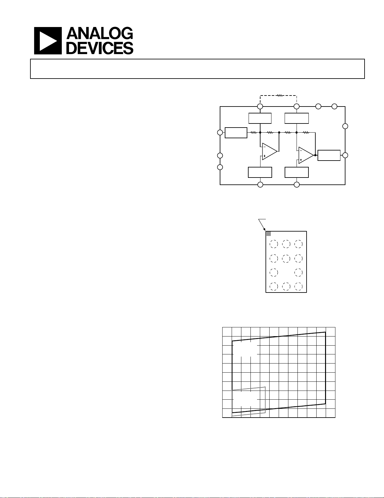
AD8235
CONNECTION DIAGRAM
R
REF
NC
NC
C1
B2
D2
ESD
PROTECTION
G
B3 A1 D1
ESD
PROTECTION
210k 210k52.5k 52.5k
OP AMP
A
ESD
PROTECTION
A3 D3
–IN
RGRG
C3
ESD
PROTECTIO N
OP AMP
ESD
PROTECTIO N
+IN
B
Figure 1.
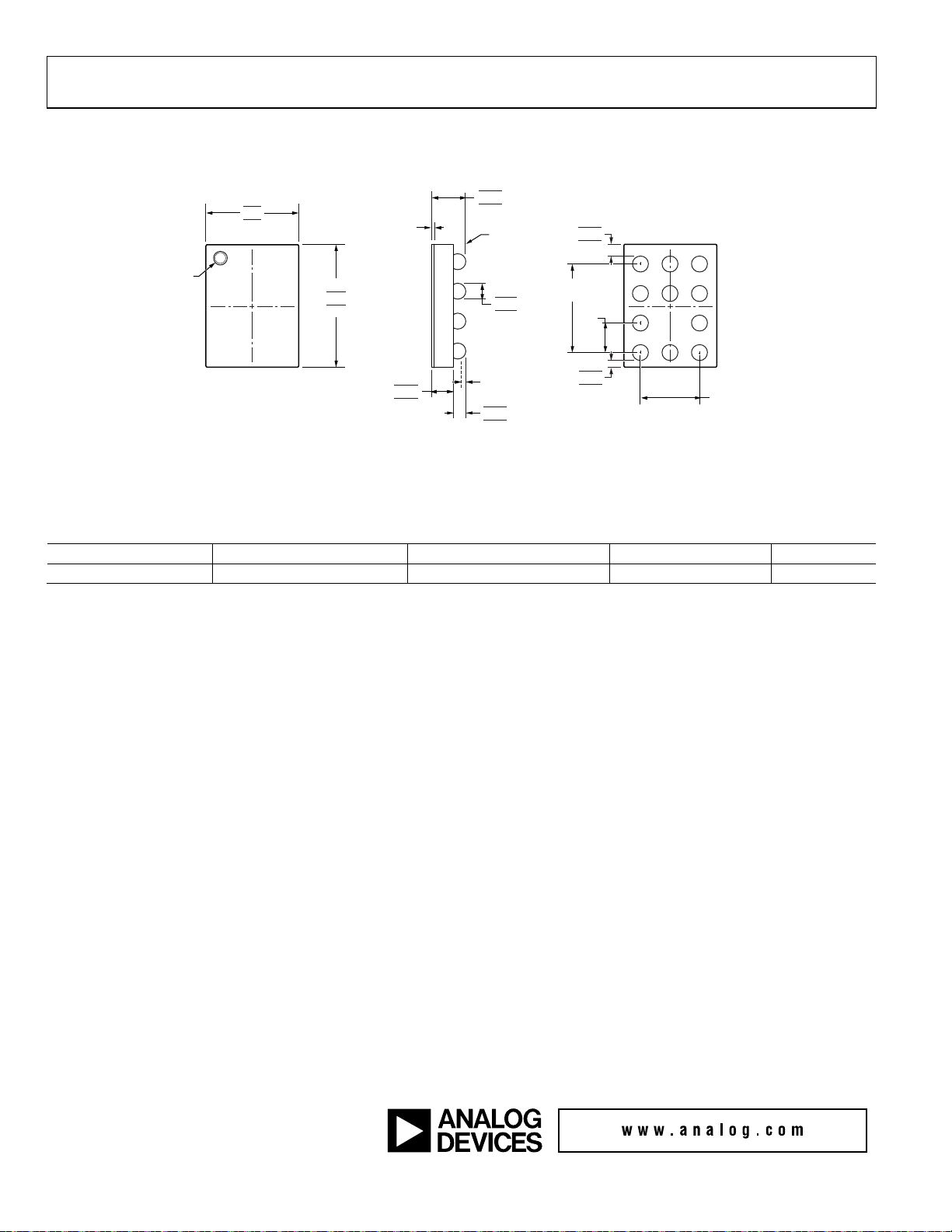
PIN CONFIGURATION
BALL A1
INDICATOR
1
23
+V
S
A
V
OUT
B
REF
C
–V
S
D
(BALL SIDE DOW N)
Not to Scal e
NC = NO CONNECT
Figure 2. 11-Ball WLCSP (CB-11-1)
5.0
4.5
(V)
4.0
3.5
3.0
2.5
2.0
1.5
1.0
INPUT COMMON-MODE VOLTAGE
0.5
G = 5
V
= 5V
S
V
= 2.5V
REF
G = 5
= 1.8V
V
S
V
= 0.9V
REF
0
OUTPUT VOLTAGE (V)
Figure 3. Wide Common-Mode Voltage Range vs. Output Voltage
SDN
NC
NC
TOP VIEW
–IN
RG
RG
+IN
08211-004
+V
S
ESD
PROTECTION
AD8235
–V
S
A2
B1
5.55.00.5–0.5 1.5 2.0 3.0 4.0 4.50 1.0 2.5 3.5
SDN
V
OUT
8211-001
8211-002
Rev. 0
Information furnished by Analog Devices is believed to be accurate and reliable. However, no
responsibility is assumed by Analog Devices for its use, nor for any infringements of patents or other
rights of third parties that may result from its use. Specifications subject to change without notice. No
license is granted by implication or otherwise under any patent or patent rights of Analog Devices.
Trademarks and registered trademarks are the property of their respective owners.
One Technology Way, P.O. Box 9106, Norwood, MA 02062-9106, U.S.A.
Tel: 781.329.4700 www.analog.com
Fax: 781.461.3113 Inc. All rights reserved. ©2009 Analog Devices,

AD8235
TABLE OF CONTENTS
Features .............................................................................................. 1
Applications ....................................................................................... 1
General Description ......................................................................... 1
Connection Diagram ....................................................................... 1
Pin Configuration ............................................................................. 1
Revision History ............................................................................... 2
Specifications ..................................................................................... 3
Absolute Maximum Ratings ............................................................ 7
Thermal Resistance ...................................................................... 7
Pin Configuration and Function Descriptions ............................. 8
Typical Performance Characteristics ............................................. 9
Theory of Operation ...................................................................... 14
Basic Operation .......................................................................... 14
Gain Selection ............................................................................. 14
Shutdown Feature ....................................................................... 15
Layout Recommendations ........................................................ 15
Reference Terminal .................................................................... 16
Power Supply Regulation and Bypassing ................................ 16
Input Bias Current Return Path ............................................... 17
Input Protection ......................................................................... 17
RF Interference ........................................................................... 17
Common-Mode Input Voltage Range ..................................... 18
Applications Information .............................................................. 19
AC-Coupled Instrumentation Amplifier ................................ 19
Low Power Heart Rate Monitor ............................................... 19
Outline Dimensions ....................................................................... 20
Ordering Guide .......................................................................... 20
REVISION HISTORY
8/09—Revision 0: Initial Version
Rev. 0 | Page 2 of 20

AD8235
SPECIFICATIONS
+VS = 5 V, −VS = 0 V (GND), V
Table 1.
Parameter Test Conditions Min Typ Max Unit
COMMON-MODE REJECTION RATIO (CMRR) VS = ±2.5 V, V
CMRR DC VCM = −1.8 V to +1.8 V
G = 5 90 94 dB
G = 10 90 100 dB
G = 100 100 110 dB
G = 200 100 110 dB
NOISE
Voltage Noise Spectral Density, RTI f = 1 kHz, G = 5 76 nV/√Hz
RTI, 0.1 Hz to 10 Hz
G = 5 4 μV p-p
G = 200 4 μV p-p
Current Noise 15 fA/√Hz
VOLTAGE OFFSET
Input Offset, VOS 2.5 mV
Average Temperature Coefficient (TC) −40°C to +125°C 0.7 μV/°C
Offset RTI vs. Supply (PSR) VS = 1.8 V to 5 V
G = 5 100 120 dB
G = 10 110 126 dB
G = 100 110 130 dB
G = 200 110 130 dB
INPUT CURRENT
Input Bias Current 1 50 pA
Overtemperature −40°C to +85°C 100 pA
−40°C to +125°C 600 pA
Input Offset Current 0.5 25 pA
Overtemperature −40°C to +85°C 50 pA
−40°C to +125°C 130 pA
DYNAMIC RESPONSE
Small Signal Bandwidth, −3 dB
G = 5 23 kHz
G = 10 9 kHz
G = 100 0.8 kHz
G = 200 0.4 kHz
Settling Time 0.01% V
G = 5 444 μs
G = 10 456 μs
G = 100 992 μs
G = 200 1816 μs
Slew Rate
G = 5 to 100 9 mV/μs
= 2.5 V, TA = 25°C, G = 5, R
REF
= 4 V step
OUT
= 100 k to GND, SDN pin tied to +VS, unless otherwise noted.
LOAD
= 0 V
REF
Rev. 0 | Page 3 of 20

AD8235
Parameter Test Conditions Min Typ Max Unit
GAIN
Gain Range G = 5 + 420 kΩ/RG 5 200
Gain Error VS = ±2.5 V, V
= 0 V, V
REF
= −2 V to +2 V
OUT
G = 5 0.005 0.05 %
G = 10 0.03 0.2 %
G = 100 0.06 0.2 %
G = 200 0.15 0.3 %
Nonlinearity RL = 10 kΩ or 100 kΩ
G = 5 2 10 ppm
G = 10 1.2 10 ppm
G = 100 0.5 10 ppm
G = 200 0.5 10 ppm
Gain vs. Temperature −40°C to +125°C
G = 5 0.35 1.5 ppm/°C
G > 10 −50 ppm/°C
INPUT
Differential Impedance 440||1.6 GΩ||pF
Common-Mode Impedance 110||6.2 GΩ||pF
Input Voltage Range −40°C to +125°C 0 +VS V
OUTPUT
Output Voltage High, VOH R
= 100 kΩ 4.98 4.99 V
L
−40°C to +125°C 4.98 V
R
= 10 kΩ 4.9 4.95 V
L
−40°C to +125°C 4.9 V
Output Voltage Low, VOL R
= 100 kΩ 2 5 mV
L
−40°C to +125°C 5 mV
R
= 10 kΩ 10 25 mV
L
−40°C to +125°C 30 mV
Short-Circuit Limit, ISC ±55 mA
REFERENCE INPUT
RIN −IN, +IN = 0 V 210 kΩ
IIN 20 nA
Voltage Range −VS +VS V
Gain to Output 1 V/V
SHUTDOWN OPERATION
Shutdown current 6 500 nA
−40°C to +125°C 1.5 μA
SDN PIN INPUT VOLTAGE RANGE
VOH −40°C to +125°C +VS − 0.5 +VS V
VOL −40°C to +125°C −VS −VS + 0.5 V
POWER SUPPLY
Operating Range 1.8 5.5 V
Quiescent Current 30 40 μA
Overtemperature −40°C to +125°C 50 μA
TEMPERATURE RANGE
For Specified Performance −40 +125 °C
1
Although the specifications of the AD8235 list only low to midrange gains, gains can be set beyond 200.
1
V/V
Rev. 0 | Page 4 of 20

AD8235
+VS = 1.8 V, −VS = 0 V (GND), V
Table 2.
Parameter Test Conditions Min Typ Max Unit
COMMON-MODE REJECTION RATIO (CMRR) VS = ±0.9 V, V
CMRR DC VCM = −0.6 V to +0.6 V
G = 5 90 94 dB
G = 10 90 100 dB
G = 100 100 110 dB
G = 200 100 110 dB
NOISE
Voltage Noise Spectral Density, RTI f = 1 kHz, G = 5 76 nV/√Hz
RTI, 0.1 Hz to 10 Hz
G = 5 4 μV p-p
G = 200 4 μV p-p
Current Noise 15 fA/√Hz
VOLTAGE OFFSET
Input Offset, VOS 2.5 mV
Average Temperature Coefficient (TC) −40°C to +125°C 0.7 μV/°C
Offset RTI vs. Supply (PSR) VS = 1.8 V to 5 V
G = 5 100 120 dB
G = 10 110 126 dB
G = 100 110 130 dB
G = 200 110 130 dB
INPUT CURRENT
Input Bias Current 1 50 pA
Overtemperature −40°C to +85°C 100 pA
−40°C to +125°C 600 pA
Input Offset Current 0.5 25 pA
Overtemperature −40°C to +85°C 50 pA
−40°C to +125°C 130 pA
DYNAMIC RESPONSE
Small Signal Bandwidth, –3 dB
G = 5 23 kHz
G = 10 9 kHz
G = 100 0.8 kHz
G = 200 0.4 kHz
Settling Time 0.01% V
G = 5 143 μs
G = 10 178 μs
G = 100 1000 μs
G = 200 1864 μs
Slew Rate
G = 5 to 100 11 mV/μs
= 0.9 V, TA = 25°C, G = 5, R
REF
= 1.4 V step
OUT
= 100 k to GND, SDN pin tied to +VS, unless otherwise noted.
LOAD
= 0 V
REF
Rev. 0 | Page 5 of 20

AD8235
Parameter Test Conditions Min Typ Max Unit
GAIN
Gain Range G = 5 + 420 kΩ/RG 5 200
Gain Error VS = ±0.9 V, V
= 0 V, V
REF
= −0.6 V to +0.6 V
OUT
G = 5 0.005 0.05 %
G = 10 0.03 0.2 %
G = 100 0.06 0.2 %
G = 200 0.15 0.3 %
Nonlinearity RL = 10 kΩ or 100 kΩ
G = 5 1 10 ppm
G = 10 1 10 ppm
G = 100 0.5 10 ppm
G = 200 0.4 10 ppm
Gain vs. Temperature −40°C to +125°C
G = 5 0.35 1.5 ppm/°C
G > 10 −50 ppm/°C
INPUT
Differential Impedance 440||1.6 GΩ||pF
Common-Mode Impedance 110||6.2 GΩ||pF
Input Voltage Range −40°C to +125°C 0 +VS V
OUTPUT
Output Voltage High, VOH R
= 100 kΩ 1.78 1.79 V
L
−40°C to +125°C 1.78 V
R
= 10 kΩ 1.65 1.75 V
L
−40°C to +125°C 1.65 V
Output Voltage Low, VOL R
= 100 kΩ 2 5 mV
L
−40°C to +125°C 5 mV
R
= 10 kΩ 12 25 mV
L
−40°C to +125°C 25 mV
Short-Circuit Limit, ISC ±6 mA
REFERENCE INPUT
RIN −IN, +IN = 0 V 210 kΩ
IIN 20 nA
Voltage Range −VS +VS V
Gain to Output 1 V/V
SHUTDOWN OPERATION
Shutdown Current 6 500 nA
−40°C to +125°C 1.5 μA
SDN PIN INPUT VOLTAGE RANGE
VOH −40°C to +125°C +VS − 0.5 +VS V
VOL −40°C to +125°C −VS −VS + 0.5 V
TEMPERATURE RANGE
For Specified Performance −40 +125 °C
1
Although the specifications of the AD8235 list only low to midrange gains, gains can be set beyond 200.
1
V/V
Rev. 0 | Page 6 of 20

AD8235
ABSOLUTE MAXIMUM RATINGS
Table 3.
Parameter Rating
Supply Voltage 6 V
Output Short-Circuit Current 55 mA
Input Voltage (Common Mode) ±VS
Differential Input Voltage ±VS
Storage Temperature Range −65°C to +125°C
Operating Temperature Range −40°C to +125°C
Junction Temperature 125°C
ESD
Human Body Model 1.5 kV
Charge Device Model 0.5 kV
Machine Model 200 V
Stresses above those listed under Absolute Maximum Ratings
may cause permanent damage to the device. This is a stress
rating only; functional operation of the device at these or any
other conditions above those indicated in the operational
section of this specification is not implied. Exposure to absolute
maximum rating conditions for extended periods may affect
device reliability.
THERMAL RESISTANCE
θ
is specified for the worst-cas
JA
lder
so ed in a circuit board for surface-mount packages. This
was measured using a standard 4-layer board, unless otherwis
specified.
Table 4. Th
Package Type PCB
11-Ball WLCSP CB-11-1 1S0P
1
Simulated thermal numbers per JESD51-9:
1-layer PCB (1S0P), low effective thermal conductivity test board.
2
4-layer PCB (2S2P), high effective thermal co
ermal Resistance
ESD CAUT
ION
e conditions, that is, a device
Power (W) θJA (°C/W)
1
0.25 139.1
1.25 130
2
2S2P
0.25 69.5
1.25 68.3
nductivity test board.
e
Rev. 0 | Page 7 of 20

AD8235
PIN CONFIGURATION AND FUNCTION DESCRIPTIONS
BALLA1
INDICATOR
1
23
+V
S
A
V
OUT
B
REF
C
–V
S
D
(BALL SIDE DOWN)
Not to Scal e
NC = NO CONNECT
Figure 4. Pin Configuration (Top View Looking Through Package)
Table 5. Pin Function Descriptions
Pin No. Mnemonic Description
A1 +VS Positive Power Supply Terminal.
B1 V
Output Terminal.
OUT
C1 REF Reference Voltage Terminal. Drive this terminal with a low impedance voltage source to level-shift the output.
D1 −VS Negative Power Supply Terminal.
A2 SDN Shutdown Pin. Tie to −VS for shutdown. Tie to +VS for normal operation.
B2, D2 NC No Connect. Leave both pins floating. Should not connect to any potential.
A3 −IN Negative Input Terminal (True Differential Input).
B3, C3 RG Gain Setting Terminals. Place resistor across the RG pins.
D3 +IN Positive Input Terminal (True Differential Input).
SDN
NC
NC
TOP VIEW
–IN
RG
RG
+IN
08211-004
Rev. 0 | Page 8 of 20

AD8235
TYPICAL PERFORMANCE CHARACTERISTICS
G = 5, +VS = 5 V, V
= 2.5 V, RL = 100 kΩ tied to GND, TA = 25°C, SDN pin connected to +VS, unless otherwise noted
REF
2400
2100
1800
1500
1200
900
NUMBER OF UNITS
600
300
0
–40 –30 0 10 40
CMRR (µV/V)
20 30–20 –10
Figure 5. CMRR Distribution
400
350
300
250
200
150
NUMBER OF UNITS
100
50
0
–2000–3000 –1000 0 1000 2000 30 00
V
(µV)
OSI
Figure 6. Typical Distribution of Input Offset Voltage
1k
GAIN = 5
1s/DIV5µV/DIV
08211-105
08211-008
Figure 8. 0.1 Hz to 10 Hz RTI Voltage Noise
GAIN = 200
08211-005
5µV/DIV
1s/DIV
08211-009
Figure 9. 0.1 Hz to 10 Hz RTI Voltage Noise
140
100
NOISE (nV/ Hz)
10
1 10 100 1k 10k
GAIN = 200
FREQUENCY ( Hz)
GAIN = 5
BANDWIDTH
Figure 7. Voltage Noise Spectral Density vs. Frequency
LIMITED
08211-007
Rev. 0 | Page 9 of 20
120
100
80
60
PSRR (dB)
40
20
0
0.1 1 10 100 1k 10k 100k
FREQUNCY (Hz)
GAIN = 200
GAIN = 10
GAIN = 5
GAIN = 100
INTERNAL
CLIPPING
Figure 10. Positive PSRR vs. Frequency, RTI,
= ±0.9 V, ±2.5 V, V
V
S
REF
= 0 V
8211-010

AD8235
120
GAIN = 100
100
80
60
PSRR (dB)
40
20
GAIN = 10
GAIN = 5
GAIN = 200
10
5
0
CMRR (µV/V)
–5
0
10.1
10 100 1k 10k 100k
FREQUENCY (Hz)
Figure 11. Negative PSRR vs. Frequency, RTI, VS = ±0.9 V, ±2.5 V, V
120
100
80
60
CMRR (dB)
40
20
0
1010.1 100k
100 1k 10k
FREQUENCY (Hz)
GAIN = 200
GAIN = 100
GAIN = 10
GAIN = 5
Figure 12. CMRR vs. Frequency, RTI
120
100
80
REF
= 0 V
08211-012
–10
–40 –20 0 20 40 60 80 100 120
08211-011
TEMPERATURE (°C)
8211-014
Figure 14. Change in CMRR vs. Temperature, G = 5, Normalized at 25°C
60
50
GAIN = 200
40
GAIN = 100
30
GAIN = 10
20
10
GAIN = 5
GAIN (dB)
0
–10
–20
–30
–40
10 1M
100 1k 10k 100k
FREQUENCY (Hz)
08211-015
Figure 15. Gain vs. Frequency, VS = 1.8 V, 5 V
6
5
4
60
CMRR (dB)
40
20
0
0.1 1 100k
10 100 1k 10k
FREQUENCY (Hz)
GAIN = 200
GAIN = 5
GAIN = 100
GAIN = 10
Figure 13. CMRR vs. Frequency, 1 kΩ Source Imbalance, RTI
08211-013
Rev. 0 | Page 10 of 20
3
(V p-p)
OUT
V
2
1
0
1 10 100 1k 10k 100k
FREQUENCY (Hz)
Figure 16. Maximum Output Voltage vs. Frequency
8211-016

AD8235
R
= 100k TIED TO GND
LOAD
R
= 10k TIED TO GND
LOAD
NONLI NEARIT Y (5ppm/DIV)
VS = 5V
0.5 1.0 1.5 2.0 2.5 3.0 3.5 4.0 4.5
OUTPUT VO LTAGE (V )
Figure 17. Gain Nonlinearity, G = 5
TWO CURVES REPRE SENTED:
R
= 10k AND 100k TIED TO GND
LOAD
NONLI NEARIT Y (2ppm/DIV)
VS = 5V
0.5 1.0 1.5 2.0 2.5 3.0 3.5 4.0 4.5
OUTPUT VO LTAGE (V )
Figure 18. Gain Nonlinearity, G = 10
TWO CURVES REPRE SENTED:
R
= 10k AND 100k TIED TO GND
LOAD
NONLI NEARIT Y (2ppm/DIV)
VS = 5V
0.5 1.0 1.5 2.0 2.5 3.0 3.5 4.0 4.5
OUTPUT VO LTAGE (V )
Figure 19. Gain Nonlinearity, G = 200
5.0
4.5
4.0
3.5
3.0
2.5
2.0
1.5
1.0
INPUT COMMO N-MODE VOL TAGE (V)
0.5
08211-017
(0.01V, 4. 24V)
(0.01V, 0.27V)
0
–0.5 5.5
00.5 2.01. 51.0 2. 5 3.0 3.5 4.0 4.5 5.0
OUTPUT VO LTAGE (V )
(4.98V, 4. 737V)
(4.98V, 0. 767V)
08211-020
Figure 20. Input Common-Mode Voltage Range vs. Output Voltage,
= 5 V, V
G = 5, V
S
5.0
4.5
4.0
3.5
3.0
2.5
2.0
1.5
1.0
INPUT COMMON-MODE VOLTAGE (V)
0.5
08211-018
(0.01V, 4. 25V)
(0.01V, 0. 026V)
0
0 0.51.01.52.02.53.03.54.04.55.0
–0.5 5.5
OUTPUT VO LTAGE (V )
= 2.5 V
REF
(4.994V, 4. 75V)
(4.994V, 0.076V)
08211-021
Figure 21. Input Common-Mode Voltage Range vs. Output Voltage,
G = 200, V
1.8
1.6
1.4
1.2
1.0
0.8
0.6
0.4
INPUT COMMO N-MODE VOL TAGE (V)
0.2
08211-019
(0.0069V, 1. 52V)
(0.0069V, 0. 09V)
0
00.2 0.80.60.4 1.0 1.2 1.4 1.6 1.8–0.2 2.0
= 5 V, V
S
OUTPUT VO LTAGE (V )
= 2.5 V
REF
(1.78V, 1. 704V)
(1.78V, 0.274V)
08211-022
Figure 22. Input Common-Mode Voltage Range vs. Output Voltage,
G = 5, V
= 1.8 V, V
S
= 0.9 V
REF
Rev. 0 | Page 11 of 20

AD8235
V
V
V
V
V
1.8
1.6
1.4
1.2
1.0
0.8
0.6
0.4
INPUT COMMO N-MODE VOL TAGE (V)
0.2
(0.03V, 1.533V)
(0.03V, 0. 103V)
0
00.2 0.80.60.4 1.0 1.2 1.4 1.6 1.8–0.2 2.0
OUTPUT VO LTAGE (V )
Figure 23. Input Common-Mode Voltage Range vs. Output Voltage,
= 1.8 V, V
S
+25°C
+
–0.001
–0.002
–0.003
S
+125°C
G = 200, V
+85°C
–40°C
(1.75V, 1. 705V)
(1.75V, 0. 275V)
= 0.9 V
REF
2V/DI
444s TO 0. 01%
308211-02
1ms/DIV
8211-026
Figure 26. Large Signal Pulse Response and Settling Time,
= ±2.5 V, V
V
S
= 0 V, R
REF
= 10 kΩ to V
LOAD
REF
+0.003
OUTPUT VOLTAGE SWING (V)
+0.002
REFERRED TO SUPPLY VOL TAGE
+0.001
+125°C
–V
S
1.8
2.32.83.33.84.34.8
+25°C+85°C
–40°C
SUPPLY VOLTAGE (V)
Figure 24. Output Voltage Swing vs. Supply Voltage,
+
–0.1
–0.2
–
0
+0.003
+0.002
OUTPUT VOLT AGE SWING (V)
REFERRED TO SUPPLY VOL TAGE
+0.001
–V
= ±0.9 V, ±2.5 V, V
V
S
S
+85°C
+125°C
.
3
+125°C
S
1k 100k
+25°C
+85°C
= 0 V, R
REF
–40°C
+25°C
= 100 kΩ Tied to −VS
LOAD
–40°C
10k
R
()
LOAD
Figure 25. Output Voltage Swing vs. Load Resistance,
= ±0.9 V, ±2.5 V, V
V
S
= 0 V, R
REF
= 100 kΩ Tied to −VS
LOAD
700mV/DI
143.2s TO 0.01%
024
08211-
1ms/DIV
8211-027
Figure 27. Large Signal Pulse Response and Settling Time,
= ±0.9 V, V
V
S
20mV/DI
08211-025
= 0 V, R
REF
100µs/DIV
= 10 kΩ to V
LOAD
REF
8211-028
Figure 28. Small Signal Pulse Response, G = 5,
V
= ±2.5 V, V
S
= 0 V, R
REF
= 100 kΩ to V
LOAD
, CL = 100 pF
REF
Rev. 0 | Page 12 of 20

AD8235
V
V
V
R
A
500
400
300
20mV/DI
100µs/DIV
Figure 29. Small Signal Pulse Response, G = 5, C
= ±0.9 V, V
V
S
20mV/DI
= 0 V, R
REF
1ms/DIV
= 100 kΩ to V
LOAD
Figure 30. Small Signal Pulse Response, G = 200,
= 100 pF, VS = 2.5 V, V
C
L
= 0 V, R
REF
= 100 kΩ to V
LOAD
= 100 pF,
L
REF
REF
8211-029
8211-030
200
SETTLING TIME (µs)
100
0
04
123
OUTPUT VOLTAGE STEP SIZE (V)
08211-032
Figure 32. Settling Time vs. Output Voltage Step Size,
V
= ±2.5 V, V
S
40
38
36
)
34
32
ENT (µ
30
28
26
SUPPLY CUR
24
22
20
–40 –25 –10 5 20 35 50 65 80 95 110 125
= 0 V, R
REF
TEMPERATURE (°C)
= 10 kΩ Tied to V
LOAD
1.8V
5V
REF
8211-033
Figure 33. Total Supply Current vs. Temperature
600
500
400
300
20mV/DI
1ms/DIV
Figure 31. Small Signal Pulse Response, G = 200,
= 100 pF, VS = 0.9 V, V
C
L
= 0 V, R
REF
LOAD
= 100 kΩ to V
200
SUPPLY CURRENT (n A)
100
0
–100
8211-031
–40 –25 –10 5 20 35 50 65 80 95 110 125
TEMPERATURE (° C)
Figure 34. Total Supply Current During Shutdown vs. Temperature
REF
VS = 5V
= 1.8V
V
S
-043
0 8211
Rev. 0 | Page 13 of 20

AD8235
V
THEORY OF OPERATION
R
REF
C1
PROTECTION
ESD
B3 C3
ESD
PROTECTION
210k 210k52.5k 52.5k
G
PROTECTION
ESD
+V
RGRG
A1
–V
S
S
D1
SDN
A2
OP AMP
NC
NC
B2
D2
PROTECTION
A
ESD
A3 D3
–IN
Figure 35. Simplified Schematic
The AD8235 is a monolithic, two-op amp instrumentation
amplifier. It is designed for low power, portable applications
where size and low quiescent current are paramount. The
AD8235 is offered in a WLCSP package, minimizing layout
area. Additional features that make this part optimal for
portable applications include a rail-to-rail input and output
stage that offers more dynamic range when operating on low
voltage batteries. Unlike traditional rail-to-rail input amplifiers
that use a complementary differential pair stage and suffer from
nonlinearity, the AD8235 uses a novel architecture to internally
boost the supply rail, allowing the amplifier to operate rail-torail yet still deliver a low 0.5 ppm of nonlinearity. In addition,
the two-op amp instrumentation amplifier architecture offers a
wide operational common-mode voltage range. Additional
information is provided in the Common-Mode Input Voltage
Range section. Precision, laser-trimmed resistors provide the
AD8235 with a high CMRR of 90 dB (minimum) at G = 5 and
gain accuracy of 0.05% (maximum).
BASIC OPERATION
The AD8235 amplifies the difference between its positive input
(+IN) and its negative input (−IN). The REF pin allows the user
to level-shift the output signal. This is convenient when interfacing
to a filter or analog-to-digital converter (ADC). The basic setup
is shown in Figure 36. Figure 39 shows an example configuration
for operating the AD8235 with dual supplies. The equation for
the AD8235 is as follows:
V
= G × (VINP − VINM) + VREF
OUT
If no gain setting resistor is installed, the default gain, G, is 5.
The Gain Selection section describes how to program the gain, G.
OP AMP
ESD
PROTECTION
ESD
B
PROTECTION
V
B1
OUT
AD8235
+IN
VINP
GAIN SETTING
RESISTOR
VINM
+IN
RG
RG
–IN
8211-034
5
SDN
+V
AD8235
–V
S
S
REF
0.1µF
OUT
V
REF
V
OUT
08211-035
Figure 36. Basic Setup
GAIN SELECTION
Placing a resistor across the RG terminals sets the gain of the
AD8235. The gain may be derived by referring to Tab le 6 or by
using the following equation:
k420
R
G
Table 6. Gains Achieved Using 1% Resistors
1% Standard Table Value of RG (kΩ) Calculated Gain
422 6.0
210 7.0
140 8.0
105 9.0
84.5 10.0
28 20.0
9.31 50.1
4.42 100.0
2.15 200.3
The AD8235 defaults to G = 5 when no gain resistor is used.
Gain accuracy is determined by the absolute tolerance of R
The TC of the external gain resistor increases the gain drift of
the instrumentation amplifier. Gain error and gain drift are at
a minimum when the gain resistor is not used.
5
−=G
.
G
Rev. 0 | Page 14 of 20

AD8235
SHUTDOWN FEATURE
The AD8235 includes a shutdown pin (SDN) that further
enhances the flexibility and ease of use in portable applications
where power consumption is critical. A logic level signal can be
applied to this pin to switch to shutdown mode, even when the
supply is still on.
When connecting the SDN pin to +V
within +V
− 0.5 V, the AD8235 operates in its normal condition
S
and, therefore, draws approximately 40 µA of supply current.
When connecting the SDN pin to −V
0.5 V, the AD8235 operates in shutdown mode and, therefore,
draws less than 500 nA of supply current, offering considerable
power savings.
In cases where the AD8235 is operating in shutdown mode, if
a voltage potential exists at the REF pin, and there is a load to
at the output of the part, some additional current draw is
−V
S
noticeable. In this mode, a path from the REF pin to −V
leading to some additional current draw from the reference.
Typically, this current is negligible because the output of the
AD8235 is driving a high impedance node, such as the input of
an ADC.
LAYOUT RECOMMENDATIONS
The critical board design parameters, as it pertains to a WLCSP
package, are pad opening, pad type, pad finish, and board
thickness.
Pad Opening
Based on the IPC (Institute for Printed Circuits) standard, the
pad opening equals the UBM (Under Bump Metallurgy)
opening. The typical pad openings for the AD8235 shown in
Figure 37 are:
• 250 µm (0.5 mm pitch WLCSP)
The solder mask opening is 100 m plus the pad opening (or
350 µm in the case of the AD8235). The trace width should be
less than two-thirds of the pad opening. Increasing the trace
width can cause reduction in the stand-off height of the solder
bump. Therefore, maintaining the proper trace width ratio is
important to ensure the reliability of the solder connections.
or applying a voltage
S
, or any voltage within −VS +
S
exists,
S
TRACE
WIDTH
PAD OP E NI N G
MASK OPENING
Figure 37. Pad Opening
0 8211-044
Pad Type
For the actual board fabrication, the following types of
pads/land patterns are used for surface mount assembly:
• Nonsolder mask defined (NSMD). The metal pad on the
PCB (to which the I/O is attached) is smaller than the
solder mask opening.
• Solder mask defined (SMD). The solder mask opening is
smaller than the metal pad.
Because the copper etching process has tighter control than the
solder mask opening process, NSMD is preferred over SMD.
The solder mask opening on NSMD pads is larger than the
copper pads, allowing the solder to attach to the sides of the
copper pad and improving the reliability of the solder joints.
Pad Finish
The finish layer on the metal pads has a significant effect on
assembly yield and reliability. The typical metal pad finishes
used are organic surface preservative (OSP) and electroless
nickel immersion gold (ENIG). The thickness of the OSP finish
on a metal pad is 0.2 m to 0.5 m. This finish evaporates during
the reflow soldering process and interfacial reactions occur
between the solder and metal pad. The ENIG finish consists
of 5 m of electroless nickel and 0.02 m to 0.05 µm of gold.
During reflow soldering, the gold layer dissolves rapidly, followed
by reaction between the nickel and solder. It is extremely important
to keep the thickness of gold below 0.05 m to prevent the
formation of brittle intermetallic compounds.
Rev. 0 | Page 15 of 20

AD8235
V
Board Thickness
Typical board thicknesses used in the industry range from
0.4 mm to 1.6 mm and are most applicable for the AD8235. The
thickness selected depends on the required robustness of the
populated system assembly. The thinner board results in smaller
shear stress range, creep shear strain range, and creep strain
energy density range in the solder joints under the thermal
loading. Therefore, the thinner build-up board leads to longer
thermal fatigue life of solder joints [John H. Lau and S.W. Ricky
1
Lee]
Grounding
The output voltage of the AD8235 is developed with respect to
the potential on the reference terminal, REF. To ensure the most
accurate output, the trace from the REF pin should either be
connected to the AD8235 local ground (see Figure 39) or
connected to a voltage that is referenced to the AD8235 local
ground (Figure 36).
REFERENCE TERMINAL
The reference terminal, REF, is at one end of a 210 kΩ resistor
(see Figure 35). The output of the instrumentation amplifier
is referenced to the voltage on the REF terminal; this is useful
when the output signal needs to be offset to voltages other than
common. For example, a voltage source can be tied to the REF
pin to level-shift the output so that the AD8235 can interface
with an ADC. The allowable reference voltage range is a function
of the gain, common-mode input, and supply voltages. The REF
pin should not exceed either +V
For best performance, especially in cases where the output is not
measured with respect to the REF terminal, source impedance to
the REF terminal should be kept low because parasitic resistance
can adversely affect CMRR and gain accuracy. Figure 38
demonstrates how an op amp is configured to provide a low
source impedance to the REF terminal when a midscale
reference voltage is desired.
1
John H. Lau and S.W. Ricky Lee, “Effects of Build-Up Printed Circuit Board
Thickness on the Solder Joint Reliability of a Wafer Level Chip Scale Package
(WLCSP),” IEEE Transactions on Components and Packaging Technologies,
Vol.25, No.1, March 2002, pages 3-14.
or −VS by more than 0.5 V.
S
INCORRECT
AD8235
REF
V
Figure 38. Driving the REF Pin
V
CORRECT
AD8235
+
OP AMP
–
REF
08211-036
POWER SUPPLY REGULATION AND BYPASSING
The AD8235 has high power supply rejection ration (PSRR).
However, for optimal performance, a stable dc voltage should be
used to power the instrumentation amplifier. Noise on the supply
pins can adversely affect performance. As in all linear circuits,
bypass capacitors must be used to decouple the amplifier.
A 0.1 µF capacitor should be placed close to each supply pin.
A 10 µF tantalum capacitor can be used farther away from the
part (see Figure 39). In most cases, it can be shared by other
precision integrated circuits.
+
S
0.1µF 10µF
SDN
+IN
V
AD8235
–IN
Figure 39. Supply Decoupling, REF, and Output Referred to Ground
REF
0.1µF 10µF
–V
S
OUT
LOAD
–V
S
08211-037
Rev. 0 | Page 16 of 20

AD8235
V
V
V
+
S
+
S
AD8235
REF
–V
S
TRANSFORMER
+V
S
C
AD8235
REF
–V
S
AC-COUPLED
Figure 40. Creating an I
INPUT BIAS CURRENT RETURN PATH
The AD8235 input bias current is extremely small at less than
50 pA. Nonetheless, the input bias current must have a return
path to common. When the source, such as a transformer,
cannot provide a return current path, one should be created
(see Figure 40).
INPUT PROTECTION
All terminals of the AD8235 are protected against ESD. In addition,
the input structure allows for dc overload conditions a diode drop
above the positive supply and a diode drop below the negative
supply. Voltages beyond a diode drop of the supplies cause the
ESD diodes to conduct and enable current to flow through the
diode. Therefore, an external resistor should be used in series
with each of the inputs to limit current for voltages above +V
In either scenario, the AD8235 safely handles a continuous 6 mA
current at room temperature.
For applications where the AD8235 encounters extreme
overload voltages, as in cardiac defibrillators, external series
resistors and low leakage diode clamps, such as BAV199Ls,
FJH1100s, or SP720s, should be used.
.
S
AD8235
REF
–V
S
TRANSFORMER
+V
S
C
f
HIGH-PASS
BIAS
=
2RC
Path
1
R
AD8235
R
AC-COUP LED
REF
–V
S
8211-038
RF INTERFERENCE
RF rectification is often a problem in applications where there are
large RF signals. The problem appears as a small dc offset voltage.
The AD8235, by its nature, has a 3.1 pF gate capacitance, C
each input. Matched series resistors form a natural low-pass filter
that reduces rectification at high frequency (see Figure 41). The
relationship between external, matched series resistors and the
internal gate capacitance is expressed as
FilterFreq
FilterFreq
DIFF
CM
0.1µF 10µF
R
R
1
=
RCπ
2
1
=
RCπ
2
G
+IN
–IN
G
SDN
+
S
C
G
AD8235
–V
S
C
G
–V
REF
S
V
OUT
G
, at
0.1µF 10µF
–V
S
8211-039
Figure 41. RFI Filtering Without External Capacitors
Rev. 0 | Page 17 of 20

AD8235
V
To eliminate high frequency common-mode signals while using
smaller source resistors, a low-pass RC network can be placed
at the input of the instrumentation amplifier (see Figure 42).
The filter limits the input signal bandwidth according to the
following relationship:
FilterFreq+=
FilterFreq
Mismatched C
DIFF
=
CM
capacitors result in mismatched low-pass filters.
C
1
)
C+2(2
CCRπ
D
1
CCRπ
+
GC
GC
)(2
The imbalance causes the AD8235 to treat what is a commonmode signal as a differential signal. To reduce the effect of
mismatched external C
than 10× C
. This sets the differential filter frequency lower than
C
capacitors, select a value of CD greater
C
the common-mode frequency.
+
S
R
4.02k
R
4.02k
0.1µF
C
1nF
C
10nF
C
D
1nF
C
C
Figure 42. RFI Suppression
SDN
+IN
AD8235
–IN
REF
10µF
V
OUT
08211-040
COMMON-MODE INPUT VOLTAGE RANGE
The common-mode input voltage range is a function of the
input voltages, reference voltage, supplies, and the output of
Internal Op Amp A. Figure 35 shows the internal nodes of the
AD8235. Figure 20 to Figure 23 show the common-mode
voltage ranges for typical supply voltages and gains.
If the supply voltages and reference voltage are not represented
in Figure 20 to Figure 23, the following methodology can be
used to calculate the acceptable common-mode voltage range:
1.
Adhere to the input, output, and reference voltage ranges
shown in Tab l e 1 and Ta ble 2 .
2.
Calculate the output of Internal Op Amp A. The following
equation calculates this output:
5
⎛
A
⎜
4
⎝
V
⎞
DIFF
−=
V
CM
⎟
2
⎠
kΩ52.5
R
G
where:
V
is defined as the difference in input voltages,
DIFF
V
= VINP − VINM.
DIFF
V
is defined as the common-mode voltage,
CM
V
= (VINP + VINM)/2.
CM
If no gain setting resistor, R
3.
Keep A within 10 mV of either supply rail. This is valid over
, is installed, set RG to infinity.
G
the −40°C to +125°C temperature range.
−V
+ 10 mV < A < +VS – 10 mV
S
V
REF
−−
V
DIFF
4
Rev. 0 | Page 18 of 20

AD8235
V
V
–
V
APPLICATIONS INFORMATION
AC-COUPLED INSTRUMENTATION AMPLIFIER
An integrator can be tied to the AD8235 in feedback to create a
high-pass filter, as shown in Figure 43. This circuit can be used
to reject dc voltages and offsets. At low frequencies, the impedance
of the capacitor, C, is high. Therefore, the gain of the integrator
is high. DC voltage at the output of the AD8235 is inverted and
gained by the integrator. The inverted signal is injected back into
the REF pin, nulling the output. In contrast, at high frequencies,
the integrator has low gain because the impedance of C is low.
Voltage changes at high frequencies are inverted but at a low
gain. The signal is injected into the REF pins, but it is not enough to
null the output. At very high frequencies, the capacitor appears as
a short. The op amp is at unity gain. High frequency signals are,
therefore, allowed to pass.
When a signal exceeds f
pass filtered input signal.
+
S
0.1µF
SDN
+IN
AD8235
–IN
+V
S
10µF
Figure 43. AC-Coupled Circuit
RA LA
RL
, the AD8235 outputs the high-
HIGH-PASS
=
+V
S
AD8603
+2.5V
AD8235
IN-AMP
–2.5V
+2.5V
1
2RC
SDN
REF
953k
953k
0.1µF
+2.5V
–2.5V
f
HIGH- PASS
C
0.1µF
0.1µF
1k
R
+2.5
100k
4.7µF
AD8609
V
REF
08211-041
1k
20k
AD8609
1k
LOW POWER HEART RATE MONITOR
The low power and small size of the AD8235 make it an excellent
choice for heart rate monitors. As shown in Figure 44, the
AD8235 measures the biopotential signals from the body. It
rejects common-mode signals and serves as the primary gain
stage set at G = 5. The 4.7 µF capacitor and the 100 k resistor
set the −3 dB cutoff of the high-pass filter that follows the
instrumentation amplifier. It rejects any differential dc offsets
that may develop from the half-cell overpotential of the electrode.
A secondary gain stage, set at G = 403, amplifies the ECG signal,
which is then sent into a second-order, low-pass, Bessel filter
with −3 dB cutoff at 48 Hz. The 324 resistor and 1 F capacitor
serve as an antialiasing filter. The 1 µF capacitor also serves as a
charge reservoir for the ADC switched capacitor input stage.
This circuit was designed and tested using the AD8609, low
power, quad op amp. The fourth op amp is configured as a Schmitt
trigger to indicate if the right arm or left arm electrodes fall off
the body. Used in conjunction with the 953 k resistors at the
inputs of the AD8235, the resistors pull the inputs apart when
the electrodes fall off the body. The Schmitt trigger sends an
active low signal to indicate a leads off condition.
The reference electrode (right leg) is set tied to ground. Likewise,
the shield of the electrode cable is also tied to ground. Some
portable heart rate monitors do not have a third electrode. In
such cases, the negative input of the AD8235 can be tied to GND.
Note that this circuit is shown, solely, to demonstrate the capability
of the AD8235. Additional effort must be made to ensure
compliance with medical safety guidelines.
2.5
5k
LEADS OFF DETECTIO N
AD8609
402k
INTERRUPT
24.9k
680nF
4.02k
220nF
+2.5V
AD8609
–2.5V
LEADS OFF
0.1µF
324
0.1µF
1µF
10-BIT ADC
MCU + ADC
–2.5V
08211-042
Figure 44. Example Low Power Heart Rate Monitor Schematic
Rev. 0 | Page 19 of 20
AD8235
OUTLINE DIMENSIONS
0.657
(CB-11-1)
0.602
0.546
SEATING
PLANE
0.330
0.310
0.290
0.04 MAX
COPLANARITY
0.280
0.250
0.220
1.50
REF
0.348
0.328
0.308
0.50
REF
0.230
0.212
0.192
3
2
BOTTOM VIEW
(BALL SI DE UP)
1
A
B
C
D
1.00
REF
060409-A
1.61
BALL A1
IDENTIFIER
1.57
1.53
TOP VIEW
(BALL SIDE DOWN)
2.08
2.04
2.00
0.020
REF
0.355
0.330
0.304
Figure 45. 11-Ball, Backside-Coated, Wafer Level Chip Scale Package [WLCSP]
Dimensions shown in millimeters
ORDERING GUIDE
Model Temperature Range Package Description Package Option Branding
AD8235ACBZ-P7
1
Z = RoHS Compliant Part.
1
−40°C to + 125°C 11-Ball [WLCSP] CB-11-1 H20
©2009 Analog Devices, Inc. All rights reserved. Trademarks and
registered trademarks are the property of their respective owners.
D08211-0-8/09(0)
Rev. 0 | Page 20 of 20
 Loading...