

Single-Supply, Rail-to-Rail
FEATURES
True single-supply operation
Input voltage range extends below ground
Output swings rail-to-rail
Single-supply capability from 5 V to 30 V
Dual-supply capability from ±2.5 V to ±15 V
High load drive
Capacitive load drive of 350 pF, G = +1
Minimum output current of 15 mA
Excellent ac performance for low power
800 µA maximum quiescent current per amplifier
Unity-gain bandwidth: 1.8 MHz
Slew rate of 3 V/s
Good dc performance
800 µV maximum input offset voltage
2 µV/°C typical offset voltage drift
25 pA maximum input bias current
Low noise
13 nV/√Hz @ 10 kHz
No phase inversion
Low Power FET-Input Op Amp
AD822-EP
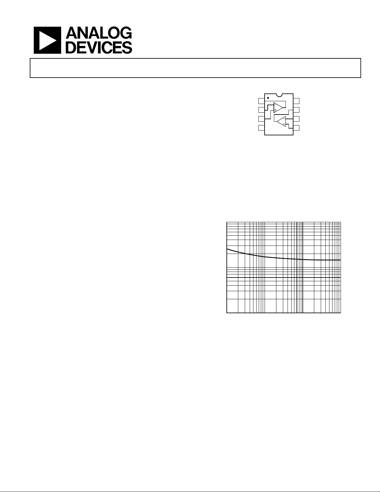
CONNECTION DIAGRAM
1
OUT1
2
–IN1
+IN1
3
4
V–
AD822-EP
Figure 1. 8-Lead SOIC_N (R Suffix)
GENERAL DESCRIPTION
The AD822-EP is a dual precision, low power FET input op
amp that can operate from a single supply of 5 V to 30 V or dual
supplies of ±2.5 V to ±15 V. It has true single-supply capability
with an input voltage range extending below the negative rail,
allowing the AD822 to accommodate input signals below
ground in the single-supply mode. Output voltage swing
extends to within 10 mV of each rail, providing the maximum
output dynamic range.
100
8
V+
OUT2
7
–IN2
6
5
+IN2
09208-001
ENHANCED PRODUCT FEATURES
Supports defense and aerospace applications (AQEC
standard)
Military temperature range (−55°C to +125°C)
Controlled manufacturing baseline
One assembly/test site
One fabrication site
Enhanced product change notification
Qualification data available on request
APPLICATIONS
Photodiode preamps
Active filters
12-bit to 14-bit data acquisition systems
Low power references and regulators
10
INPUT VOLTAGE NOISE (nV/√Hz)
1
10 10k
Figure 2. Input Voltage Noise vs. Frequency
100
FREQUENCY (Hz)
1k
09208-002
Offset voltage of 800 μV maximum, offset voltage drift of 2 μV/°C,
input bias currents below 25 pA, and low input voltage noise
provide dc precision with source impedances up to a gigaohm.
The 1.8 MHz unity-gain bandwidth, –93 dB THD at 10 kHz,
and 3 V/μs slew rate are provided with a low supply current of
800 μA per amplifier.
Rev. 0
Information furnished by Analog Devices is believed to be accurate and reliable. However, no
responsibility is assumed by Anal og Devices for its use, nor for any infringements of patents or ot her
rights of third parties that may result from its use. Specifications subject to change without notice. No
license is granted by implication or otherwise under any patent or patent rights of Analog Devices.
Trademarks and registered trademarks are the property of their respective owners.
One Technology Way, P.O. Box 9106, Norwood, MA 02062-9106, U.S.A.
Tel: 781.329.4700 www.analog.com
Fax: 781.461.3113 ©2010 Analog Devices, Inc. All rights reserved.

AD822-EP
TABLE OF CONTENTS
Features.............................................................................................. 1
Enhanced Product Features ............................................................ 1
Applications....................................................................................... 1
Connection Diagram ....................................................................... 1
General Description ......................................................................... 1
Revision History ............................................................................... 2
Specifications..................................................................................... 4
REVISION HISTORY
6/10—Revision 0: Initial Version
Absolute Maximum Ratings ......................................................... 10
Thermal Resistance.................................................................... 10
ESD Caution................................................................................ 10
Typical Performance Characteristics........................................... 11
Outline Dimensions....................................................................... 18
Ordering Guide .......................................................................... 18
Rev. 0 | Page 2 of 20
AD822-EP
The AD822-EP drives up to 350 pF of direct capacitive load as a
follower and provides a minimum output current of 15 mA.
This allows the amplifier to handle a wide range of load conditions.
Its combination of ac and dc performance, plus the outstanding
load drive capability, results in an exceptionally versatile amplifier
for the single-supply user.
The AD822-EP operates over the military temperature range of
−55°C to +125°C.
The AD822-EP is offered in an 8-lead SOIC_N package.
Full details about this enhanced product are available in the
AD822 data sheet, which should be consulted in conjunction
with this data sheet.
100
90
5V
V
OUT
10
0%
0V
(GND)
1V 20µs
........
.
....
....
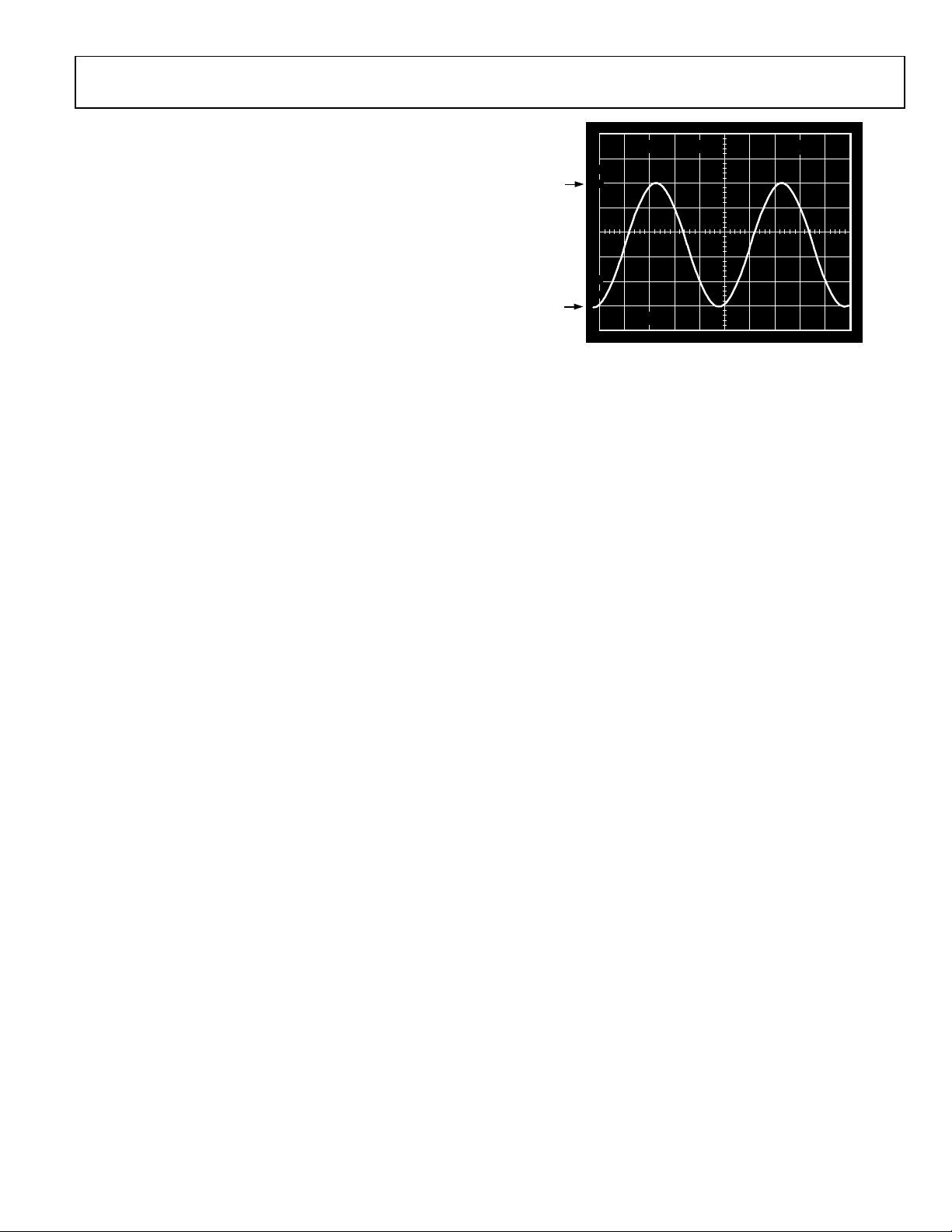
1V
Figure 3. Gain-of-2 Amplifier; V
= 2.5 V Sine Centered at 1.25 V, RL = 100 Ω
V
IN
1V
.... .... .... ....
.... .... .... ....
....
....
= 5 V, 0 V,
S
.... .... ....
.... .... ....
9208-003
Rev. 0 | Page 3 of 20

AD822-EP
SPECIFICATIONS
VS = 0 V, 5 V @ TA = 25°C, VCM = 0 V, V
Table 1.
T Grade
Parameter Test Conditions/Comments Min Typ Max Unit
DC PERFORMANCE
Initial Offset 0.1 0.8 mV
Maximum Offset Over Temperature 0.5 1.2 mV
Offset Drift 2 μV/°C
Input Bias Current VCM = 0 V to 4 V 2 25 pA
At T
0.5 6 nA
MAX
Input Offset Current 2 20 pA
At T
0.5 nA
MAX
Open-Loop Gain V
R
T
to T
MIN
400 V/mV
MAX
R
T
to T
MIN
80 V/mV
MAX
R
T
to T
MIN
10 V/mV
MAX
NOISE/HARMONIC PERFORMANCE
Input Voltage Noise
f = 0.1 Hz to 10 Hz 2 μV p-p
f = 10 Hz 25 nV/√Hz
f = 100 Hz 21 nV/√Hz
f = 1 kHz 16 nV/√Hz
f = 10 kHz 13 nV/√Hz
Input Current Noise
f = 0.1 Hz to 10 Hz 18 fA p-p
f = 1 kHz 0.8 fA/√Hz
Harmonic Distortion RL = 10 kΩ to 2.5 V
f = 10 kHz V
DYNAMIC PERFORMANCE
Unity-Gain Frequency 1.8 MHz
Full Power Response V
Slew Rate 3 V/μs
Settling Time
To 0.1% V
To 0.01% V
MATCHING CHARACTERISTICS
Initial Offset 1.0 mV
Maximum Offset Over Temperature 1.6 mV
Offset Drift 3 μV/°C
Input Bias Current 20 pA
Crosstalk @ f = 1 kHz RL = 5 kΩ −130 dB
Crosstalk @ f = 100 kHz RL = 5 kΩ −93 dB
= 0.2 V, unless otherwise noted.
OUT
= 0.2 V to 4 V
OUT
= 100 kΩ 500 1000 V/mV
L
= 10 kΩ 80 150 V/mV
L
= 1 kΩ 15 30 V/mV
L
= 0.25 V to 4.75 V −93 dB
OUT
p-p = 4.5 V 210 kHz
OUT
= 0.2 V to 4.5 V 1.4 μs
OUT
= 0.2 V to 4.5 V 1.8 μs
OUT
Rev. 0 | Page 4 of 20

AD822-EP
T Grade
Parameter Test Conditions/Comments Min Typ Max Unit
INPUT CHARACTERISTICS
Input Voltage Range1, T
Common-Mode Rejection Ratio (CMRR) VCM = 0 V to 2 V 66 80 dB
T
to T
MIN
V
MAX
Input Impedance
Differential 1013||0.5 Ω||pF
Common Mode 1013||2.8 Ω||pF
OUTPUT CHARACTERISTICS
Output Saturation Voltage2
VOL − VEE I
T
to T
MIN
10 mV
MAX
VCC − VOH I
T
to T
MIN
20 mV
MAX
VOL − VEE I
T
to T
MIN
80 mV
MAX
VCC − VOH I
T
to T
MIN
160 mV
MAX
VOL – VEE I
T
to T
MIN
1000 mV
MAX
VCC − VOH I
T
to T
MIN
1900 mV
MAX
Operating Output Current 15 mA
T
to T
MIN
12 mA
MAX
Capacitive Load Drive 350 pF
POWER SUPPLY
Quiescent Current, T
Power Supply Rejection V+ = 5 V to 15 V 66 80 dB
T
to T
MIN
1
This is a functional specification. Amplifier bandwidth decreases when the input common-mode voltage is driven in the range (V+ − 1 V) to V+. Common-mode error
voltage is typically less than 5 mV with the common-mode voltage set at 1 V below the positive supply.
2
VOL − VEE is defined as the difference between the lowest possible output voltage (VOL) and the negative voltage supply rail (VEE). VCC − VOH is defined as the difference
between the highest possible output voltage (VOH) and the positive supply voltage (VCC).
66 dB
MAX
MIN
to T
MIN
to T
−0.2 +4 V
MAX
= 0 V to 2 V 66 dB
CM
= 20 μA 5 7 mV
SINK
= 20 μA 10 14 mV
SOURCE
= 2 mA 40 55 mV
SINK
= 2 mA 80 110 mV
SOURCE
= 15 mA 300 500 mV
SINK
= 15 mA 800 1500 mV
SOURCE
1.24 1.6 mA
MAX
Rev. 0 | Page 5 of 20

AD822-EP
VS = ±5 V @ TA = 25°C, VCM = 0 V, V
Table 2.
T Grade
Parameter Test Conditions/Comments Min Typ Max Unit
DC PERFORMANCE
Initial Offset 0.1 0.8 mV
Maximum Offset Over Temperature 0.5 1.5 mV
Offset Drift 2 μV/°C
Input Bias Current VCM = −5 V to +4 V 2 25 pA
At T
0.5 6 nA
MAX
Input Offset Current 2 20 pA
At T
0.5 nA
MAX
Open-Loop Gain V
R
T
to T
MIN
400 V/mV
MAX
R
T
to T
MIN
80 V/mV
MAX
R
T
to T
MIN
10 V/mV
MAX
NOISE/HARMONIC PERFORMANCE
Input Voltage Noise
f = 0.1 Hz to 10 Hz 2 μV p-p
f = 10 Hz 25 nV/√Hz
f = 100 Hz 21 nV/√Hz
f = 1 kHz 16 nV/√Hz
f = 10 kHz 13 nV/√Hz
Input Current Noise
f = 0.1 Hz to 10 Hz 18 fA p-p
f = 1 kHz 0.8 fA/√Hz
Harmonic Distortion RL = 10 kΩ
f = 10 kHz V
DYNAMIC PERFORMANCE
Unity-Gain Frequency 1.9 MHz
Full Power Response V
Slew Rate 3 V/μs
Settling Time
to 0.1% V
to 0.01% V
MATCHING CHARACTERISTICS
Initial Offset 1.0 mV
Maximum Offset Over Temperature 3 mV
Offset Drift 3 μV/°C
Input Bias Current 25 pA
Crosstalk @ f = 1 kHz RL = 5 kΩ −130 dB
Crosstalk @ f = 100 kHz RL = 5 kΩ −93 dB
INPUT CHARACTERISTICS
Input Voltage Range1, T
MIN
to T
Common-Mode Rejection Ratio (CMRR) VCM = −5 V to +2 V 66 80 dB
T
to T
MIN
V
MAX
Input Impedance
Differential 1013||0.5 Ω||pF
Common Mode 1013||2.8 Ω||pF
= 0 V, unless otherwise noted.
OUT
= −4 V to +4 V
OUT
= 100 kΩ 400 1000 V/mV
L
= 10 kΩ 80 150 V/mV
L
= 1 kΩ 20 30 V/mV
L
= ±4.5 V −93 dB
OUT
p-p = 9 V 105 kHz
OUT
= 0 V to ±4.5 V 1.4 μs
OUT
= 0 V to ±4.5 V 1.8 μs
OUT
−5.2 +4 V
MAX
= −5 V to +2 V 66 dB
CM
Rev. 0 | Page 6 of 20

AD822-EP
T Grade
Parameter Test Conditions/Comments Min Typ Max Unit
OUTPUT CHARACTERISTICS
Output Saturation Voltage2
VOL − VEE I
T
to T
MIN
10 mV
MAX
VCC − VOH I
T
to T
MIN
20 mV
MAX
VOL − VEE I
T
to T
MIN
80 mV
MAX
VCC − VOH I
T
to T
MIN
VOL − V
T
MIN
160 mV
MAX
I
EE
to T
1000 mV
MAX
VCC − VOH I
T
to T
MIN
1900 mV
MAX
Operating Output Current 15 mA
T
to T
MIN
12 mA
MAX
Capacitive Load Drive 350 pF
POWER SUPPLY
Quiescent Current, T
MIN
to T
1.3 1.6 mA
MAX
Power Supply Rejection VSY = ±5 V to ±15 V 66 80 dB
T
to T
MIN
1
This is a functional specification. Amplifier bandwidth decreases when the input common-mode voltage is driven in the range (V+ − 1 V) to V+. Common-mode error
voltage is typically less than 5 mV with the common-mode voltage set at 1 V below the positive supply.
2
VOL − VEE is defined as the difference between the lowest possible output voltage (VOL) and the negative voltage supply rail (VEE). VCC − VOH is defined as the difference
between the highest possible output voltage (VOH) and the positive supply voltage (VCC).
66 dB
MAX
= 20 μA 5 7 mV
SINK
= 20 μA 10 14 mV
SOURCE
= 2 mA 40 55 mV
SINK
= 2 mA 80 110 mV
SOURCE
= 15 mA 300 500 mV
SINK
= 15 mA 800 1500 mV
SOURCE
Rev. 0 | Page 7 of 20

AD822-EP
VS = ±15 V @ TA = 25°C, VCM = 0 V, V
Table 3.
T Grade
Parameter Test Conditions/Comments Min Typ Max Unit
DC PERFORMANCE
Initial Offset 0.4 2 mV
Maximum Offset Over Temperature 0.5 3 mV
Offset Drift 2 μV/°C
Input Bias Current VCM = 0 V 2 25 pA
V
At T
V
MAX
Input Offset Current 2 20 pA
At T
0.5 nA
MAX
Open-Loop Gain V
R
T
to T
MIN
500 V/mV
MAX
R
T
to T
MIN
100 V/mV
MAX
R
T
to T
MIN
20 V/mV
MAX
NOISE/HARMONIC PERFORMANCE
Input Voltage Noise
f = 0.1 Hz to 10 Hz 2 μV p-p
f = 10 Hz 25 nV/√Hz
f = 100 Hz 21 nV/√Hz
f = 1 kHz 16 nV/√Hz
f = 10 kHz 13 nV/√Hz
Input Current Noise
f = 0.1 Hz to 10 Hz 18 fA p-p
f = 1 kHz 0.8 fA/√Hz
Harmonic Distortion RL = 10 kΩ
f = 10 kHz V
DYNAMIC PERFORMANCE
Unity-Gain Frequency 1.9 MHz
Full Power Response V
Slew Rate 3 V/μs
Settling Time
to 0.1% V
to 0.01% V
MATCHING CHARACTERISTICS
Initial Offset 3 mV
Maximum Offset Over Temperature 4 mV
Offset Drift 3 μV/°C
Input Bias Current 25 pA
Crosstalk @ f = 1 kHz RL = 5 kΩ −130 dB
Crosstalk @ f = 100 kHz RL = 5 kΩ −93 dB
INPUT CHARACTERISTICS
Input Voltage Range1, T
MIN
to T
MAX
Common-Mode Rejection Ratio (CMRR) VCM = −15 V to +12 V 70 80 dB
T
to T
MIN
V
MAX
Input Impedance
Differential 1013||0.5 Ω||pF
Common Mode 1013||2.8 Ω||pF
= 0 V, unless otherwise noted.
OUT
= −10 V 40 pA
CM
= 0 V 0.5 6 nA
CM
= −10 V to +10 V
OUT
= 100 kΩ 500 2000 V/mV
L
= 10 kΩ 100 500 V/mV
L
= 1 kΩ 30 45 V/mV
L
= ±10 V −85 dB
OUT
p-p = 20 V 45 kHz
OUT
= 0 V to ±10 V 4.1 μs
OUT
= 0 V to ±10 V 4.5 μs
OUT
−15.2 +14 V
= −15 V to +12 V 70 dB
CM
Rev. 0 | Page 8 of 20

AD822-EP
T Grade
Parameter Test Conditions/Comments Min Typ Max Unit
OUTPUT CHARACTERISTICS
Output Saturation Voltage2
VOL − VEE I
T
to T
MIN
10 mV
MAX
VCC − VOH I
T
to T
MIN
20 mV
MAX
VOL − VEE I
T
to T
MIN
80 mV
MAX
VCC − VOH I
T
to T
MIN
VOL − V
T
MIN
160 mV
MAX
I
EE
to T
1000 mV
MAX
VCC − VOH I
T
to T
MIN
1900 mV
MAX
Operating Output Current 20 mA
T
to T
MIN
15 mA
MAX
Capacitive Load Drive 350 pF
POWER SUPPLY
Quiescent Current, T
MIN
to T
1.4 1.8 mA
MAX
Power Supply Rejection VSY = ±5 V to ±15 V 70 80 dB
T
to T
MIN
1
This is a functional specification. Amplifier bandwidth decreases when the input common-mode voltage is driven in the range (V+ − 1 V) to V+. Common-mode error
voltage is typically less than 5 mV with the common-mode voltage set at 1 V below the positive supply.
2
VOL − VEE is defined as the difference between the lowest possible output voltage (VOL) and the negative voltage supply rail (VEE). VCC − VOH is defined as the difference
between the highest possible output voltage (VOH) and the positive supply voltage (VCC).
70 dB
MAX
= 20 μA 5 7 mV
SINK
= 20 μA 10 14 mV
SOURCE
= 2 mA 40 55 mV
SINK
= 2 mA 80 110 mV
SOURCE
= 15 mA 300 500 mV
SINK
= 15 mA 800 1500 mV
SOURCE
Rev. 0 | Page 9 of 20

AD822-EP
ABSOLUTE MAXIMUM RATINGS
Table 4.
Parameter Rating
Supply Voltage ±18 V
Internal Power Dissipation
8-Lead SOIC_N (R)
Input Voltage
Output Short-Circuit Duration Indefinite
Differential Input Voltage ±30 V
Storage Temperature Range (R) –65°C to +150°C
Operating Temperature Range −55°C to +125°C
Maximum Junction Temperature 150°C
Lead Temperature
(Soldering, 60 sec)
Observe Maximum
Junction Temperature
((V+) + 0.2 V) to
((V−) − 20 V)
260°C
Stresses above those listed under Absolute Maximum Ratings
may cause permanent damage to the device. This is a stress
rating only; functional operation of the device at these or any
other conditions above those indicated in the operational
section of this specification is not implied. Exposure to absolute
maximum rating conditions for extended periods may affect
device reliability.
THERMAL RESISTANCE
θJA is specified for the worst-case conditions, that is, a device
soldered in a circuit board for surface-mount packages.
Table 5. Thermal Resistance
Package Type θJA θ
8-lead SOIC_N (R) 160 43 °C/W
Unit
JC
ESD CAUTION
Rev. 0 | Page 10 of 20

AD822-EP
TYPICAL PERFORMANCE CHARACTERISTICS
70
60
50
40
30
NUMBER OF U NITS
20
10
VS = 0V, 5V
5
0
V
= 0V, +5V AND ±5V
VS = ±5V
INPUT BI AS CU RRE N T ( pA)
S
0
–0.5 –0.4
–0.3 –0.2 –0.1 0
OFFSET VOLTAGE (mV)
0.10.20.30.40.5
Figure 4. Typical Distribution of Offset Voltage (390 Units)
16
V
= ±5V
14
12
10
8
% IN BIN
6
4
2
0
–12 10–10
–8 –6 –4 –2
OFFSET VOLTAGE DRIFT (µV/°C)
S
V
S
= ±15V
86420
Figure 5. Typical Distribution of Offset Voltage Drift (100 Units)
50
45
40
35
30
25
20
NUMBER OF UNI TS
15
10
5
0
0 2345678910
1
INPUT BIAS CURRE NT (pA)
Figure 6. Typical Distribution of Input Bias Current (213 Units)
–5
09208-004
–55–4
–3 –2 –1 0 1 2 3
COMMON-MODE VOLTAGE (V)
Figure 7. Input Bias Current vs. Common-Mode Voltage; V
V
= ±5 V
S
1k
100
10
1
INPUT BIAS CURRENT (p A)
0.1
–16 16–12
09208-005
–8 –4 0 4 8 12
COMMON-MODE VOLTAGE (V)
Figure 8. Input Bias Current vs. Common-Mode Voltage; V
100k
10k
1k
100
10
INPUT BI AS CURRE N T ( pA)
1
0.1
20 14040
09208-006
Figure 9. Input Bias Current vs. Temperature; V
60 80 100 120
TEMPERATURE (°C)
S
4
= 5 V, 0 V, and
S
= ±15 V
S
= 5 V, VCM = 0 V
09208-007
09208-008
09208-009
Rev. 0 | Page 11 of 20

AD822-EP
–
10M
40
VS = ±15V
1M
= 0V, +5V
V
S
V
100k
OPEN-LOOP GAIN (V/V)
10k
100 100k
1k 10k
LOAD RESI STANCE (Ω)
= 0V, +3V
S
Figure 10. Open-Loop Gain vs. Load Resistance
10M
RL = 100kΩ
OPEN-LOOP GAIN (V/V)
1M
100k
10k
–60 140–40
= 10kΩ
R
L
= 600Ω
R
L
–20 0 20 40 60 80 100 120
TEMPE RATURE (°C)
V
S
V
S
V
S
Figure 11. Open-Loop Gain vs. Temperature
= ±15V
V
S
= 0V, +5V
V
= ±15V
S
= 0V, +5V
V
= ±15V
S
= 0V, +5V
R
20
RL = 20kΩ
= 2kΩ
L
POS RAIL
NEG RAIL
= 100kΩ
L
60
POS RAIL
120 180 240
NEG RAIL
NEG RAIL
00
09208-013
0
POS
RAIL
–20
INPUT ERRO R V O LTAGE (µV)
R
–40
09208-010
03
OUTPUT VOLTAGE FROM SUPPLY RAILS (mV)
Figure 13. Input Error Voltage with Output Voltage Within 300 mV of Either
Supply Rail for Various Resistive Loads; V
1k
100
10
INPUT VOLTAGE NOISE (nV/√Hz)
1
09208-011
1 10k100
10 1k
FREQUENCY (Hz)
= ±5 V
S
09208-014
Figure 14. Input Voltage Noise vs. Frequency
300
200
100
–100
INPUT ERROR VOLTAGE (V)
–200
–300
R
0
–16 16–12
= 10kΩ
L
= 600Ω
R
L
–8 –4 0 4 8 12
OUTPUT VOLTAGE (V)
RL = 100kΩ
Figure 12. Input Error Voltage vs. Output Voltage for Resistive Loads
09208-012
Rev. 0 | Page 12 of 20
40
RL = 10kΩ
= –1
A
CL
–50
–60
–70
–80
THD (dB)
V
= ±15V; V
S
–90
V
= ±5V; V
S
–100
= 0V, +5V; V
V
S
–110
100 100k1k
OUT
OUT
V
S
= 20V p-p
= 9V p-p
OUT
= 0V, +3V; V
= 4.5V p-p
FREQUENCY ( Hz )
= 2.5V p- p
OUT
10k
Figure 15. Total Harmonic Distortion (THD) vs. Frequency
09208-015

AD822-EP
A
R
A
T
100
80
PHASE
60
40
20
OPEN-LOOP GAIN (dB)
0
RL = 2kΩ
CL = 100pF
–20
10 10M100
GAIN
1k 10k 100k 1M
FREQUENCY ( Hz )
Figure 16. Open-Loop Gain and Phase Margin vs. Frequency
1k
A
= +1
CL
= ±15V
V
S
100
10
1
100
80
60
40
20
0
–20
PHASE MARGIN ( Degrees)
90
80
70
60
50
40
30
20
COMMON-M ODE REJECTI ON (dB)
10
09208-016
0
V
S
VS = ±15V
= 0V, +3V
FREQUENCY (Hz)
= 0V, +5V
V
S
10M100 1k 10k 100k 1M10
09208-019
Figure 19. Common-Mode Rejection vs. Frequency
5
4
NEGATIVE
RAIL
3
2
+25°C
POSITIVE
RAIL
OUTPUT I M P E DANCE (Ω)
0.1
0.01
100 10M1k
10k 100k 1M
FREQUENCY (Hz)
Figure 17. Output Impedance vs. Frequency
16
12
OUTPUT SWING FROM 0TO ±VOLTS
8
4
0
–4
–8
–12
–16
051
1%
1%
0.01%
0.1%
234
SETTLING TIME (µs)
ERROR
0.01%
Figure 18. Output Swing and Error vs. Settling Time
–55°C
+125°C
210
09208-020
1
COMMON-MODE E RRO R V O LTAGE (mV)
0
09208-017
–1 3
–55°C
+125°C
COMMON-MODE VOLTAGE FROM SUPPLY RAILS (V)
Figure 20. Absolute Common-Mode Error vs. Common-Mode Voltage from
Supply Rails (V
1000
AGE (mV)
100
VS – V
TION VOL
TU
10
OUTPUT S
0
0.001 1000.01
9208-018
0.1 1 10
LOAD CURRE NT (mA)
− VCM)
S
OH
VOL – V
S
09208-021
Figure 21. Output Saturation Voltage vs. Load Current
Rev. 0 | Page 13 of 20

AD822-EP
A
A
T
T
1000
I
SOURCE
I
AGE (mV)
TION VOL
TUR
OUTPUT S
100
10
1
–60 140–40
–20 0 20 40
TEMPERATURE (°C)
SINK
I
SOURCE
I
SINK
I
SOURCE
I
SINK
60
80 100 120
Figure 22. Output Saturation Voltage vs. Temperature
= 10mA
= 10mA
= 1mA
= 1mA
= 10µA
= 10µA
09208-022
100
90
80
70
60
50
40
30
20
POWER SUPPLY REJECTION (dB)
10
0
10 10M100
+PSRR
–PSRR
1k 10k 100k 1M
FREQUENCY (Hz)
Figure 25. Power Supply Rejection vs. Frequency
09208-025
80
70
60
50
40
= 0V, +5V
V
30
20
SHORT-CIRCUI T CURRENT L IMIT ( mA)
10
0
–60 140–40 –20 0 20 40 60 80 100 120
S
V
= 0V, +3V
S
= 0V, +5V
V
S
TEMPERATURE (°C)
V
S
= ±15V
VS = ±15V
V
= 0V, +3V
S
Figure 23. Short-Circuit Current Limit vs. Temperature
1600
1400
1200
1000
800
T = +125°C
T = +25°C
T = –55°C
–OUT
30
= 2kΩ
R
1M
L
09208-026
25
VS = ±15V
20
AGE (V)
15
+
–
–
+
+
09208-023
10
OUTPUT VOL
= 0V, +5V
V
S
5
= 0V, +3V
V
S
0
10k 10M100k
FREQUENCY (Hz)
Figure 26. Large Signal Frequency Response
600
400
QUIESCENT CURRENT (µA)
200
0
4
TOTAL SUPPLY VOLTAGE (V)
Figure 24. Quiescent Current vs. Supply Voltage vs. Temperature
3632282420161208
09208-024
Rev. 0 | Page 14 of 20

AD822-EP
–
V
V
V
70
–80
–90
–100
–110
CROSSTALK (dB)
–120
–130
–140
300 1M1k 3k 10k 30k 100k 300k
FREQUENCY (Hz)
Figure 27. Crosstalk vs. Frequency
+
0.01µF
8
+
V
IN
1/2
AD822-EP
–
0.01µF
4
R
L
Figure 28. Unity-Gain Follower
100pF
100
90
10
0%
Figure 31. Large Signal Response Unity-Gain Follower; VS = ±15 V, RL = 10 kΩ
09208-028
100
90
V
OUT
09208-029
10
0%
5V 5µs
09208-032
10mV 500ns
5V 10µs
100
90
10
0%
09208-030
Figure 29. 20 V p-p, 25 kHz Sine Wave Input; Unity-Gain Follower; VS = ±15 V,
= 600 Ω
R
L
20V p-p
V
IN
2
V+
0.1µF 1µF
8
–
1/2
AD822-EP
+
3
CROSSTALK = 20 log
1
5kΩ
V
10V
OUT
OUT
20kΩ 2.2kΩ
7
AD822-EP
5kΩ
IN
1/2
V–
6
–
+
5
0.1µF 1µF
Figure 30. Crosstalk Test Circuit
09208-033
Figure 32. Small Signal Response Unity-Gain Follower; VS = ±15 V, RL = 10 kΩ
1V 2µs
100
90
10
0%
GND
09208-034
Figure 33. VS = 5 V, 0 V; Unity-Gain Follower Response to 0 V to 4 V Step
+
0.01µF
8
V
+
IN
09208-031
1/2
AD822-EP
–
4
Figure 34. Unity-Gain Follower
V
100pF
R
L
OUT
09208-035
Rev. 0 | Page 15 of 20

AD822-EP
G
Figure 36. V
10kΩ
V
IN
20kΩ
V+
0.01µF
8
–
1/2
AD822-EP
+
R
L
4
Figure 35. Gain-of-Two Inverter
100
90
10
0%
GND
= 5 V, 0 V; Unity-Gain Follower Response to 0 V to 5 V Step
S
V
OUT
100
90
10mV 2µs
100pF
09208-036
2µs1V
09208-037
10
0%
GND
Figure 38. V
100
10
GND
= 5 V, 0 V; Gain-of-2 Inverter Response to 20 mV Step,
S
Centered 20 mV Below Ground, R
1V 2µs
= 10 kΩ
L
9208-039
Figure 37. V
GND
10mV 2µs
100
90
10
0%
= 5 V, 0 V; Unity-Gain Follower Response to 40 mV Step,
S
Centered 40 mV above Ground, R
= 10 kΩ
L
09208-040
Figure 39. V
09208-038
ND
Figure 40. V
= 5 V, 0 V; Gain-of-2 Inverter Response to 2.5 V Step,
S
Centered −1.25 V Below Ground, R
500mV 10µs
100
90
10
0%
= 3 V, 0 V; Gain-of-2 Inverter, VIN = 1.25 V, 25 kHz, Sine Wave
S
Centered at −0.75 V, R
= 600 Ω
L
= 10 kΩ
L
09208-041
Rev. 0 | Page 16 of 20

AD822-EP
1V 10µs
........
.... .... .... ....
........
.... .... .... ....
1V
GND
100
90
10
0%
....
.... .... ....
....
.... .... ....
(a)
.... .... ....
....
.... .... ....
....
10µs
1V
.... .... ... ...
....
....
100
+V
s
90
10
....
.... .... .... .... ....
0%
GND
1V
1V
(b)
5V
R
P
V
IN
Figure 41. (a) Response with R
= 0 V to +VS + 200 mV
(b) V
IN
= 0 V to +VS
V
OUT
R
= 49.9 kΩ
P
= 0; VIN from 0 V to +VS
P
V
OUT
09208-042
Rev. 0 | Page 17 of 20

AD822-EP
OUTLINE DIMENSIONS
5.00 (0.1968)
4.80 (0.1890)
4.00 (0.1574)
3.80 (0.1497)
0.25 (0.0098)
0.10 (0.0040)
COPLANARITY
0.10
CONTROLLING DIMENSIONS ARE IN MILLIMETERS; INCHDIMENSIONS
(IN PARENTHESES)ARE ROUNDED-OFF MILLIMETER EQUIVALENTSFOR
REFERENCE ONLYAND ARE NOT APPROPRIATE FOR USE IN DESIGN.
85
1
1.27 (0.0500)
SEATING
PLANE
COMPLIANT TO JEDEC STANDARDS MS-012-AA
BSC
6.20 (0.2441)
5.80 (0.2284)
4
1.75 (0.0688)
1.35 (0.0532)
0.51 (0.0201)
0.31 (0.0122)
8°
0°
0.25 (0.0098)
0.17 (0.0067)
0.50 (0.0196)
0.25 (0.0099)
1.27 (0.0500)
0.40 (0.0157)
45°
012407-A
Figure 42. 8-Lead Standard Small Outline Package [SOIC_N]
Narrow Body
(R-8)
Dimensions shown in millimeters and (inches)
ORDERING GUIDE
Model1 Temperature Range Package Description Package Option
AD822TRZ-EP −55°C to +125°C 8-Lead SOIC_N R-8
AD822TRZ-EP-R7 −55°C to +125°C 8-Lead SOIC_N R-8
1
Z = RoHS Compliant Part.
SPICE model is available at www.analog.com.
Rev. 0 | Page 18 of 20

AD822-EP
NOTES
Rev. 0 | Page 19 of 20

AD822-EP
NOTES
©2010 Analog Devices, Inc. All rights reserved. Trademarks and
registered trademarks are the property of their respective owners.
D09208-0-6/10(0)
Rev. 0 | Page 20 of 20
 Loading...