Precision Gain of 5
Instrumentation Amplifier
AD8225
FEATURES
No External Components Required
Highly Stable, Factory Trimmed Gain of 5
Low Power, 1.2 mA Max Supply Current
Wide Power Supply Range (1.7 V to 18 V)
Single- and Dual-Supply Operation
Excellent Dynamic Performance
High CMRR
86 dB Min @ DC
80 dB Min to 10 kHz
Wide Bandwidth
900 kHz
4 V to 36 V Single Supply
High Slew Rate
5 V/s Min
Outstanding DC Precision
Low Gain Drift
5 ppm/C Max
Low Input Offset Voltage
150 V Max
Low Offset Drift
2 V/C Max
Low Input Bias Current
1.2 nA Max
APPLICATIONS
Patient Monitors
Current Transmitters
Multiplexed Systems
4 to 20 mA Converters
Bridge Transducers
Sensor Signal Conditioning
FUNCTIONAL BLOCK DIAGRAM
NC
–IN
+IN
–V
140
130
120
110
100
90
HIGH PERFORMANCE IN AMP
80
CMRR – dB
70
60
50
40
30
1 100k10
@ GAIN OF 5
AD8225
1
2
3
4
S
NC = NO CONNECT
100 1k 10k
FREQUENCY – Hz
8
NC
7
+V
S
6
V
OUT
5
REF
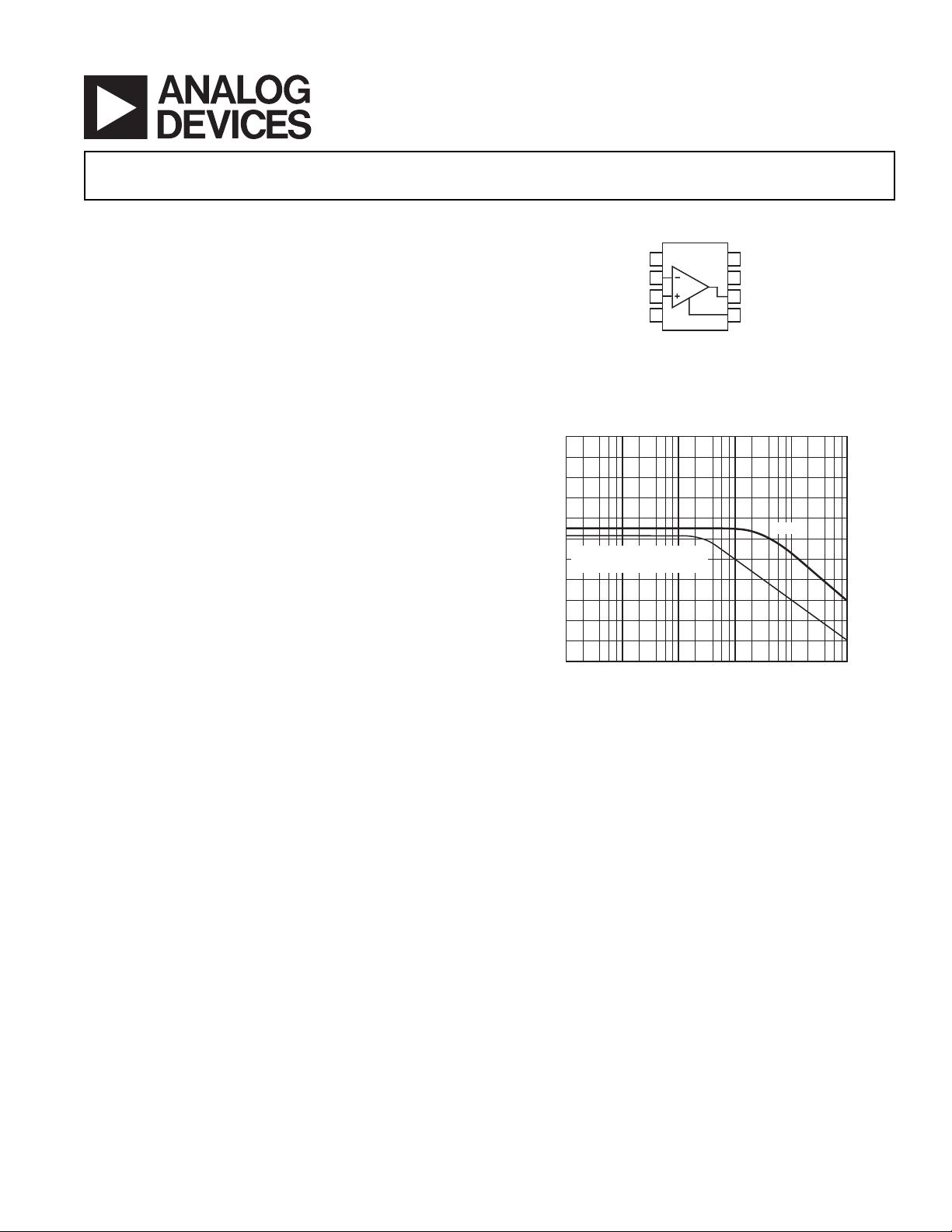
Figure 1. Typical CMRR vs. Frequency
AD8225
GENERAL DESCRIPTION
The AD8225 is an instrumentation amplifier with a fixed gain
of 5, which sets new standards of performance. The superior
CMRR of the AD8225 enables rejection of high frequency
common-mode voltage (80 dB Min @ 10 kHz). As a result,
higher ambient levels of noise from utility lines, industrial
equipment, and other radiating sources are rejected. Extended
CMV range enables the AD8225 to extract low level differential
signals in the presence of high common-mode dc voltage levels
even at low supply voltages.
Ambient electrical noise from utility lines is present at 60 Hz
and harmonic frequencies. Power systems operating at 400 Hz
create high noise environments in aircraft instrument clusters.
Good CMRR performance over frequency is necessary if power
system generated noise is to be rejected. The dc to 10 kHz
REV. A
Information furnished by Analog Devices is believed to be accurate and
reliable. However, no responsibility is assumed by Analog Devices for its
use, nor for any infringements of patents or other rights of third parties that
may result from its use. No license is granted by implication or otherwise
under any patent or patent rights of Analog Devices. Trademarks and
registered trademarks are the property of their respective companies.
CMRR performance of the AD8225 rejects noise from utility
systems, motors, and repair equipment on factory floors, switching power supplies, and medical equipment.
Low input bias currents combined with a high slew rate of 5 V/µs
make the AD8225 ideally suited for multiplexed applications.
The AD8225 provides excellent dc precision, with maximum
input offset voltage of 150 µV and drift of 2 µV/°C. Gain drift is
5ppm/°C or less.
Operating on either single or dual supplies, the fixed gain of 5
and wide input common-mode voltage range make the AD8225
well suited for patient monitoring applications.
The AD8225 is packaged in an 8-lead SOIC package and is
specified over the standard industrial temperature range, –40°C
to +85°C.
One Technology Way, P.O. Box 9106, Norwood, MA 02062-9106, U.S.A.
Tel: 781/329-4700 www.analog.com
Fax: 781/326-8703 © 2003 Analog Devices, Inc. All rights reserved.

AD8225–SPECIFICATIONS
(TA = 25C, VS = 15 V, RL = 2 k, unless otherwise noted.)
Parameter Conditions Min Typ Max Unit
GAIN
Gain 5V/V
Gain Error –0.1 +0.05 +0.1 %
Nonlinearity 2 10 ±ppm
vs. Temperature 1 5 ±ppm/°C
OFFSET VOLTAGE (RTI)
Offset Voltage 50 150 ±µV
vs. Temperature 0.3 2 ±µV/°C
vs. Supply (PSRR) 90 100 dB
INPUT
Input Operating Impedance
储
Differential 10
Common Mode 10
Input Voltage Range –V
+ 1.6 +VS – 1.0 V
S
2GΩ储pF
储
2GΩ储pF
(Common-Mode)
vs. Temperature –V
+ 2.2 +VS – 1.2 V
S
Input Bias Current 0.5 1.2 nA
vs. Temperature 3 pA/°C
Input Offset Current 0.15 0.5 nA
vs. Temperature 1.5 pA/°C
Common-Mode Rejection Ratio 86 94 dB
= T
T
A
MIN
to T
MAX
83 dB
f = 10 kHz* 80 dB
OUTPUT
Operating Voltage Range RL = 2 kΩ –VS + 1.4 +VS – 1.4 V
vs. Temperature –V
Operating Voltage Range R
= 10 kΩ –VS + 1.0 +VS – 1.1 V
L
vs. Temperature –V
+ 1.5 +VS – 1.6 V
S
+ 1.2 +VS – 1.0 V
S
Short Circuit Current 18 mA
DYNAMIC RESPONSE
Small Signal –3 dB Bandwidth 900 kHz
Full Power Bandwidth V
= 20 V p-p 75 kHz
OUT
Settling Time (0.01%) 10 V Step 3.4 µs
Settling Time (0.001%) 10 V Step 4.8 µs
Slew Rate 5 V/µs
NOISE (RTI)
Voltage 0.1 Hz to 10 Hz 1.5 µV p-p
Spectral Density, 1 kHz 45 nV/√Hz
Current 0.1 Hz to 10 Hz 4 pA p-p
Spectral Density, 1 kHz 50 fA/√Hz
REFERENCE INPUT
R
IN
I
IN
Voltage Range –V
V
, V
IN+
= 0 18 kΩ
REF
60 µA
+ 1.4 +VS – 1.4 V
S
Gain to Output 0.999 1 1.001
POWER SUPPLY
Operating Range 1.7 18 ±V
Quiescent Current 1.05 1.2 mA
TEMPERATURE RANGE
For Specified Performance –40 +85 °C
*Pin 1 connected to Pin 4. See Applications section.
Specifications subject to change without notice.
REV. A–2–

AD8225
SPECIFICATIONS
(TA = 25C, VS = 5 V, RL = 2 k, unless otherwise noted.)
Parameter Conditions Min Typ Max Unit
GAIN
Gain 5V/V
Gain Error –0.1 +0.05 +0.1 %
Nonlinearity 2 10 ±ppm
vs. Temperature 1 5 ±ppm/°C
VOLTAGE OFFSET (RTI)
Offset Voltage 125 325 ±µV
vs. Temperature 2 ±µV/°C
vs. Supply 90 100 dB
INPUT
Input Operating Impedance
Differential 10
Common-Mode 10
Input Operating Voltage Range –V
vs. Temperature –V
+ 1.6 +VS – 1.0 V
S
+ 2.1 +VS – 1.5 V
S
储
2GΩ储pF
储
2GΩ储pF
Input Bias Current 0.5 1.2 nA
vs. Temperature 3 pA/°C
Input Offset Current 0.15 0.5 nA
vs. Temperature 1.5 pA/°C
Common-Mode Rejection Ratio 86 94 dB
= T
T
A
MIN
to T
MAX
83 dB
f = 10 kHz* 80 dB
OUTPUT
Operating Voltage Range RL = 2 kΩ –VS + 0.9 +VS – 1.0 V
vs. Temperature –V
Operating Voltage Range R
= 10 kΩ –VS + 0.8 +VS – 1.0 V
L
vs. Temperature –V
+ 1.0 +VS – 1.2 V
S
+ 0.9 +VS – 1.0 V
S
Short Circuit Current 18 mA
DYNAMIC RESPONSE
Small Signal –3 dB Bandwidth 900 kHz
Full Power Bandwidth V
= 7.8 V p-p 170 kHz
OUT
Settling Time (0.01%) 7 V Step 3 µs
Settling Time (0.001%) 7 V Step 4.3 µs
Slew Rate 5 V/µs
NOISE (RTI)
Voltage 0.1 Hz to 10 Hz 1.5 µV p-p
Spectral Density, 1 kHz 45 nV/√Hz
Current 0.1 Hz to 10 Hz 4 pA p-p
Spectral Density, 1 kHz 50 fA/√Hz
REFERENCE INPUT
R
IN
I
IN
V
, V
INT
= 0 60 µA
REF
Voltage Range –V
+ 0.9 +VS – 1.0 V
S
18 kΩ
Gain to Output 0.999 1 1.001
POWER SUPPLY
Operating Range 1.7 18 ±V
Quiescent Current 1.05 1.2 mA
TEMPERATURE RANGE
For Specified Performance –40 +85 °C
*Pin 1 connected to Pin 4. See Applications section.
Specifications subject to change without notice.
REV. A
–3–

AD8225
SPECIFICATIONS
(TA = 25C, VS = 5 V, RL = 2 k, unless otherwise noted.)
Parameter Conditions Min Typ Max Unit
GAIN
Gain 5V/V
Gain Error –0.1 +0.05 +0.1 %
Nonlinearity 2 10 ±ppm
vs. Temperature 1 5 ±ppm/°C
OFFSET VOLTAGE (RTI)
Offset Voltage 150 375 ±µV
vs. Temperature 2 ±µV/°C
vs. Supply 90 100 dB
INPUT
Input Operating Impedance
Differential 10
Common Mode 10
Input Voltage Range 1.6 V
储
2GΩ储pF
储
2GΩ储pF
– 1.05 V
S
(Common-Mode)
vs. Temperature 1.7 V
– 1.0 V
S
Input Bias Current 0.5 1.2 nA
vs. Temperature 3 pA/°C
Input Offset Current 0.15 0.5 nA
vs. Temperature 1.5 pA/°C
Common-Mode Rejection Ratio 86 94 dB
= T
T
A
MIN
to T
MAX
83 dB
f = 10 kHz* 80 dB
OUTPUT
Operating Voltage Range RL = 2 kΩ 0.8 VS – 1.05 V
vs. Temperature 0.9 V
Operating Voltage Range R
= 10 kΩ 0.8 VS – 1.0 V
L
vs. Temperature 0.9 V
– 1.2 V
S
– 1.0 V
S
Short Circuit Current 18 mA
DYNAMIC RESPONSE
Small Signal –3 dB Bandwidth 900 kHz
Full Power Bandwidth V
= 3.2 V p-p 420 kHz
OUT
Settling Time (0.01%) 2 V Step 3.3 µs
Settling Time (0.001%) 2 V Step 5.1 µs
Slew Rate 5 V/µs
NOISE (RTI)
Voltage 0.1 Hz to 10 Hz 1.5 µV p-p
Spectral Density, 1 kHz 45 nV/√Hz
Current 0.1 Hz to 10 Hz 4 pA p-p
Spectral Density, 1 kHz 50 fA/√Hz
REFERENCE INPUT
R
IN
I
IN
Voltage Range 0.4 V
18 kΩ
60 µA
– 0.9 V
S
Gain to Output 0.999 1 1.001
POWER SUPPLY
Operating Range 3.4 36 V
Quiescent Current 1.05 1.2 mA
TEMPERATURE RANGE
For Specified Performance –40 +85 °C
*Pin 1 connected to Pin 4. See Applications section.
Specifications subject to change without notice.
REV. A–4–

AD8225
AMBIENT TEMPERATURE – C
1.5
1.0
0
–5080–40
POWER DISSIPATION – W
–30
–20
–10 0 10 203040506070
0.5
90
TJ = 150 C
8-LEAD SOIC PACKAGE
ABSOLUTE MAXIMUM RATINGS*
Supply Voltage . . . . . . . . . . . . . . . . . . . . . . . . . . . . . . . . ± 18 V
Internal Power Dissipation . . . . . . . . . . . . . . . . . . . . 650 mW
Input Voltage (Common-Mode) . . . . . . . . . . . . . . . . . . . . ±V
S
Differential Input Voltage . . . . . . . . . . . . . . . . . . . . . . . ±25 V
Output Short Circuit Duration . . . . . . . . . . . . . . . . Indefinite
Storage Temperature . . . . . . . . . . . . . . . . . . –65ºC to +125ºC
Operating Temperature Range . . . . . . . . . . . –40ºC to +85ºC
Lead Temperature Range (10 sec Soldering) . . . . . . . . . 300ºC
*Stresses above those listed under Absolute Maximum Ratings may cause perma-
nent damage to the device. This is a stress rating only and functional operation of
the device at these or any other conditions above those indicated in the operational
section of this specification is not implied. Exposure to absolute maximum rating
conditions for extended periods may affect device reliability.
PIN FUNCTION DESCRIPTIONS
Pin Number Mnemonic Function
1NCMay be Connected to Pin 4 to
Balance C
IN
2 –IN Inverting Input
3 +IN Noninverting Input
4 –V
S
Negative Supply Voltage
5 REF Connect to Desired Output
CMV
6V
7+V
OUT
S
Output
Positive Supply Voltage
8NC
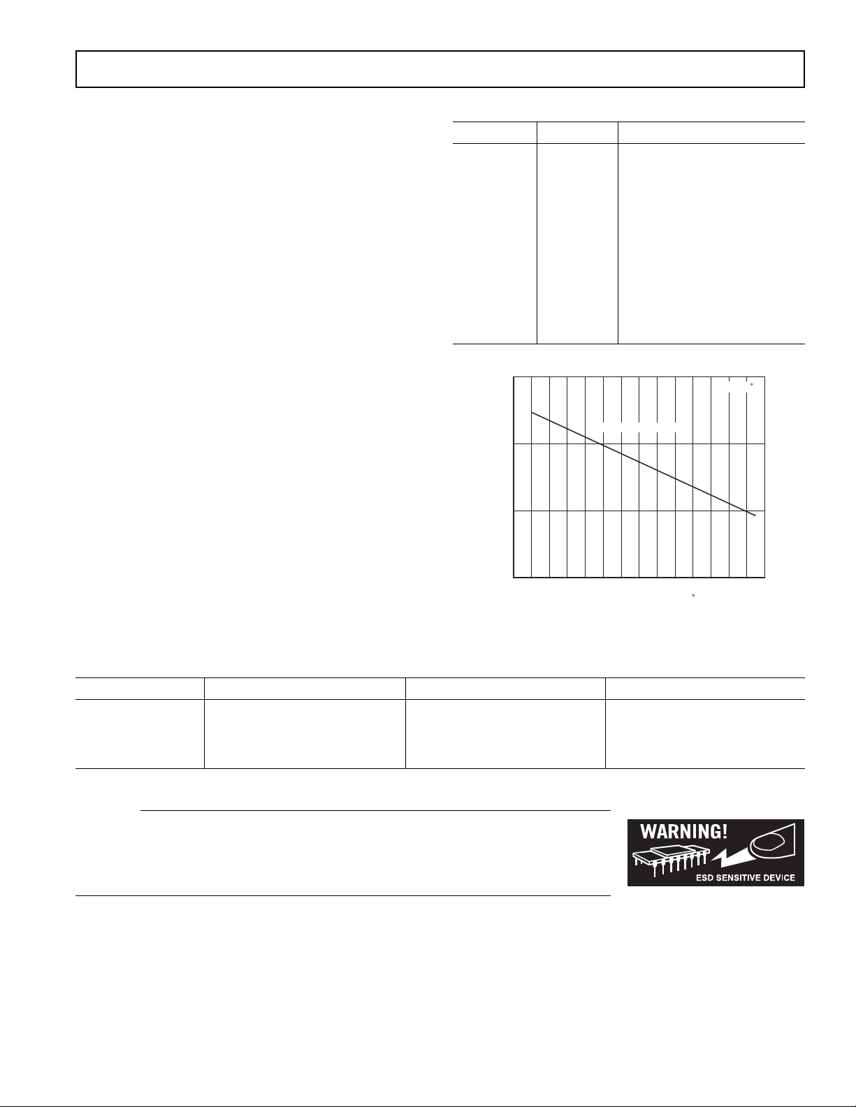
Figure 2. Maximum Power Dissipation vs. Temperature
ORDERING GUIDE
Model Temperature Range Package Description Package Options
AD8225AR –40ºC to +85ºC 8-Lead SOIC RN-8
AD8225AR-REEL –40ºC to +85ºC 8-Lead SOIC 13" REEL
AD8225AR-REEL7 –40ºC to +85ºC 8-Lead SOIC 7" REEL
AD8225-EVAL Evaluation Board RN-8
CAUTION
ESD (electrostatic discharge) sensitive device. Electrostatic charges as high as 4000 V readily
accumulate on the human body and test equipment and can discharge without detection. Although the
AD8225 features proprietary ESD protection circuitry, permanent damage may occur on devices
subjected to high energy electrostatic discharges. Therefore, proper ESD precautions are recommended
to avoid performance degradation or loss of functionality.
REV. A
–5–
 Loading...