

现货库存、技术资料、百科信息、热点资讯,精彩尽在鼎好!
Precision, Dual-Channel
FEATURES
Two channels in small 4 mm × 4 mm LFCSP
Gain set with 1 resistor per amplifier (G = 1 to 10,000)
Low noise
8 nV/√Hz @ 1 kHz
0.25 μV p-p (0.1 Hz to 10 Hz)
High accuracy dc performance (B grade)
60 μV maximum input offset voltage
0.3 μV/°C maximum input offset drift
1.0 nA maximum input bias current
126 dB minimum CMRR (G = 100)
Excellent ac performance
150 kHz bandwidth (G = 100)
13 μs settling time to 0.001%
Differential output option (single channel)
Fully specified
Adjustable common-mode output
Supply range: ±2.3 V to ±18 V
APPLICATIONS
Multichannel data acquisition for
ECG and medical instrumentation
Industrial process controls
Wheatstone bridge sensors
Differential drives for
High resolution input ADCs
Remote sensors
GENERAL DESCRIPTION
The AD8222 is a dual-channel, high performance instrumentation
amplifier that requires only one external resistor per amplifier
to set gains of 1 to 10,000.
The AD8222 is the first dual-instrumentation amplifier in the
small 4 mm × 4mm LFCSP. It requires the same board area as a
typical single instrumentation amplifier. The smaller package
allows a 2× increase in channel density and a lower cost per
channel, all with no compromise in performance.
The AD8222 can also be configured as a single-channel,
differential output instrumentation amplifier. Differential
outputs provide high noise immunity, which can be useful when
the output signal must travel through a noisy environment, such
as with remote sensors. The configuration can also be used to
drive differential input ADCs.
Instrumentation Amplifier
AD8222
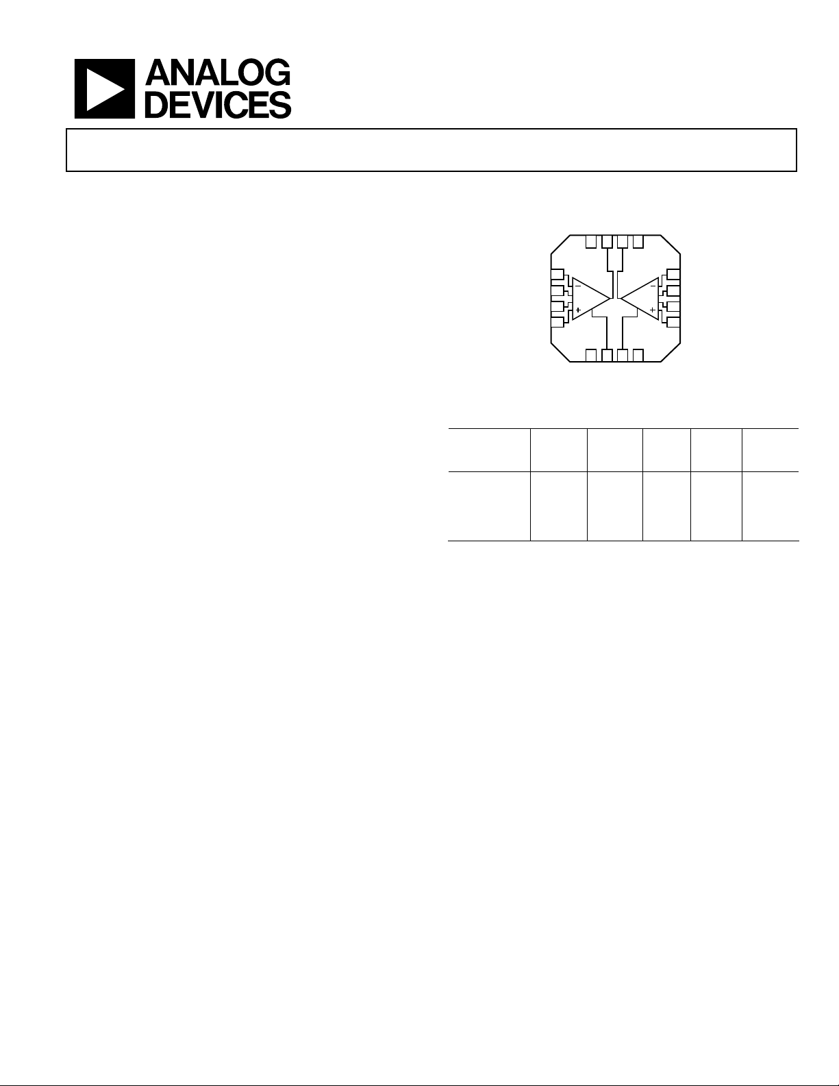
FUNCTIONAL BLOCK DIAGRAM
+VSOUT1
AD8222
1
–IN1
2
RG1
3
RG1
4
+IN1
5678
S
+V
Figure 1. 4mm × 4 mm LFCSP
Table 1. In Amps and Differential Amplifier by Category
High
Performance
AD8221
1
AD8220
AD8222
1
Rail-to-rail output.
Low
Cost
AD8553
AD6231
1
High
Voltage
AD628
AD629
The AD8222 maintains a minimum CMRR of 80 dB to 4 kHz
for all grades at G = 1. High CMRR over frequency allows the
AD8222 to reject wideband interference and line harmonics,
greatly simplifying filter requirements. The AD8222 also has a
typical CMRR drift over temperature of just 0.07 µV/V/°C at G = 1.
The AD8222 operates on both single and dual supplies and only
requires 2.2 mA maximum supply current for both amplifiers. It
is specified over the industrial temperature range of −40°C to
+85°C and is fully RoHS compliant.
For a single-channel version, see the AD8221.
S
OUT2
–V
13141516
12
–IN2
11
RG2
10
RG2
9
+IN2
S
–V
REF1
REF2
05947-001
Digital
1
Prog
Gain
AD8555
AD8556
AD8557
Mil
Grade
AD620
AD621
AD524
Low
Power
AD627
AD526
AD624
1
1
1
Rev. 0
Information furnished by Analog Devices is believed to be accurate and reliable. However, no
responsibility is assumed by Anal og Devices for its use, nor for any infringements of patents or ot her
rights of third parties that may result from its use. Specifications subject to change without notice. No
license is granted by implication or otherwise under any patent or patent rights of Analog Devices.
Trademarks and registered trademarks are the property of their respective owners.
One Technology Way, P.O. Box 9106, Norwood, MA 02062-9106, U.S.A.
Tel: 781.329.4700 www.analog.com
Fax: 781.461.3113 ©2006 Analog Devices, Inc. All rights reserved.

AD8222
TABLE OF CONTENTS
Features .............................................................................................. 1
Layout .......................................................................................... 16
Applications....................................................................................... 1
Functional Block Diagram .............................................................. 1
General Description......................................................................... 1
Revision History ............................................................................... 2
Specifications..................................................................................... 3
Absolute Maximum Ratings............................................................ 6
Thermal Resistance ...................................................................... 6
ESD Caution.................................................................................. 6
Pin Configuration and Function Descriptions............................. 7
Typical Performance Characteristics ............................................. 8
Theory of Operation ...................................................................... 15
Amplifier Architecture .............................................................. 15
Gain Selection ............................................................................. 15
Reference Terminal ....................................................................16
Solder Wash................................................................................. 17
Input Bias Current Return Path ............................................... 17
Input Protection ......................................................................... 17
RF Interference........................................................................... 18
Common-Mode Input Voltage Range..................................... 18
Applications..................................................................................... 19
Differential Output .................................................................... 19
Driving a Differential Input ADC............................................ 20
Precision Strain Gauge .............................................................. 20
Driving Cabling.......................................................................... 21
Outline Dimensions ....................................................................... 22
Ordering Guide .......................................................................... 22
REVISION HISTORY
7/06—Revision 0: Initial Version
Rev. 0 | Page 2 of 24

AD8222
SPECIFICATIONS
VS = ±15 V, V
Table 2. Single-Ended and Differential
A Grade B Grade
Parameter Conditions Min Typ Max Min Typ Max Unit
COMMON-MODE REJECTION
RATIO (CMRR)
CMRR DC to 60 Hz 1 kΩ source imbalance
G = 1 80 86 dB
G = 10 100 106 dB
G = 100 120 126 dB
G = 1000 130 140 dB
CMRR at 4 kHz
G = 1 80 80 dB
G = 10 90 100 dB
G = 100 100 110 dB
G = 1000 100 110 dB
CMRR Drift T = −40°C to +85°C, G = 1 0.07 0.07 μV/V/°C
NOISE
Voltage Noise, 1 kHz RTI Noise = √(e
Input Voltage Noise, e
Output Voltage Noise, e
RTI f = 0.1 Hz to 10 Hz
G = 1 2 2 μV p-p
G = 10 0.5 0.5 μV p-p
G = 100 to 1000 0.25 0.25 μV p-p
Current Noise f = 1 kHz 40 40 fA/√Hz
f = 0.1 Hz to 10 Hz 6 6 pA p-p
VOLTAGE OFFSET RTI VOS = (V
Input Offset, V
Overtemperature T = −40°C to +85°C 150 80 μV
Average TC 0.4 0.3 μV/°C
Output Offset, V
Overtemperature T = −40°C to +85°C 0.8 0.5 mV
Average TC 9 5 μV/°C
Offset RTI vs. Supply (PSR) VS = ±2.3 V to ±18 V
G = 1 90 110 94 110 dB
G = 10 110 120 114 130 dB
G = 100 124 130 130 140 dB
G = 1000 130 140 140 150 dB
INPUT CURRENT (PER CHANNEL)
Input Bias Current 0.5 2.0 0.2 1.0 nA
Over temperature T = −40°C to +85°C 3.0 1.5 nA
Average TC 1 1 pA/°C
Input Offset Current 0.2 1 0.1 0.5 nA
Overtemperature T = −40°C to +85°C 1.5 0.6 nA
Average TC 1 0.5 2 pA/°C
REFERENCE INPUT
R
IN
I
IN
Voltage Range −V
Gain to Output
= 0 V, TA = 25°C, G = 1, RL = 2 kΩ, unless otherwise noted.
REF
1
Output Configuration
= –10 V to +10 V
V
CM
2
+ (eNO/G)2)
NI
V
, V
, V
NI
NO
OSI
OSO
IN+
V
, V
IN+
VS = ±5 V to ±15 V 120 60 μV
VS = ±5 V to ±15 V 500 350 μV
= 0 V 8 8 nV/√Hz
IN−
REF
, V
= 0 V 75 75 nV/√Hz
IN−
REF
OSI
) + (V
/G)
OSO
20 20 kΩ
V
, V
, V
IN+
= 0 V 50 60 50 60 μA
IN−
REF
S
+V
S
−V
S
1 ± 0.0001 1 ± 0.0001
+V
S
V
V/V
Rev. 0 | Page 3 of 24

AD8222
A Grade B Grade
Parameter Conditions Min Typ Max Min Typ Max Unit
GAIN G = 1 + (49.4 kΩ/RG)
Gain Range 1 10000 1 10000 V/V
Gain Error V
G = 1 0.05 0.02 %
G = 10 0.3 0.15 %
G = 100 0.3 0.15 %
G = 1000 0.3 0.15 %
Gain Nonlinearity V
G = 1 3 10 1 5 ppm
G = 10 7 20 7 20 ppm
G = 100 7 20 7 20 ppm
Gain vs. Temperature
G = 1 3 10 2 5 ppm/°C
2
G > 1
INPUT
Input Impedance
Differential 100||2 100||2 GΩ||pF
Common Mode 100||2 100||2 GΩ||pF
Input Operating Voltage Range3VS = ±2.3 V to ±5 V −VS + 1.9 +VS − 1.1 −VS + 1.9 +VS − 1.1 V
Overtemperature T = −40°C to +85°C −VS + 2.0 +VS − 1.2 −VS + 2.0 +VS − 1.2 V
Input Operating Voltage Range3VS = ±5 V to ±18 V −VS + 1.9 +VS − 1.2 −VS + 1.9 +VS − 1.2 V
Overtemperature T = −40°C to +85°C −VS + 2.0 +VS − 1.2 −VS + 2.0 +VS − 1.2 V
OUTPUT RL = 10 kΩ
Output Swing VS = ±2.3 V to ±5 V −VS + 1.1 +VS − 1.2 −VS + 1.1 +VS − 1.2 V
Overtemperature T = −40°C to +85°C −VS + 1.4 +VS − 1.3 −VS + 1.4 +VS − 1.3 V
Output Swing VS = ±5 V to ±18 V −VS + 1.2 +VS − 1.4 −VS + 1.2 +VS − 1.4 V
Overtemperature T = −40°C to +85°C −VS + 1.6 +VS − 1.5 −VS + 1.6 +VS − 1.5 V
Short-Circuit Current 18 18 mA
POWER SUPPLY
Operating Range VS = ±2.3 V to ±18 V ±2.3 ±18 ±2.3 ±18 V
Quiescent Current (per Amplifier) 0.9 1.1 0.9 1.1 mA
Overtemperature T = −40°C to +85°C 1 1.2 1 1.2 mA
TEMPERATURE RANGE
Specified Performance −40 +85 −40 +85 °C
Operational
1
Refers to differential configuration shown in Figure 49.
2
Does not include the effects of external resistor RG.
3
One input grounded. G = 1.
4
See Typical Performance Characteristics for expected operation between 85°C to 125°C.
4
± 10 V
OUT
= –10 V to +10 V
OUT
−50 −50 ppm/°C
−40 +125 −40 +125 °C
Rev. 0 | Page 4 of 24

AD8222
VS = ±15 V, V
Table 3. Single-Ended Output Configuration—Dynamic Performance (Both Amplifiers)
A Grade B Grade
Parameter Conditions Min Typ Max Min Typ Max Unit
DYNAMIC RESPONSE
Small Signal −3 dB Bandwidth
G = 1 1200 1200 kHz
G = 10 750 750 kHz
G = 100 140 140 kHz
G =1000 15 15 kHz
Settling Time 0.01% 10 V step
G = 1 to 100 10 10 μs
G = 1000 80 80 μs
Settling Time 0.001% 10 V step
G = 1 to 100 13 13 μs
G = 1000 110 110 μs
Slew Rate
G = 1 1.5 2 1.5 2 V/μs
G = 5 to 1000 2 2.5 2 2.5 V/μs
Table 4. Differential Output Configuration
A Grade B Grade
Parameter Conditions Min Typ Max Min Typ Max Unit
DYNAMIC RESPONSE
Small Signal −3 dB Bandwidth
G = 1 1000 1000 kHz
G = 10 650 650 kHz
G = 100 140 140 kHz
G =1000 15 15 kHz
Settling Time 0.01% 10 V step
G = 1 to 100 15 15 μs
G = 1000 80 80 μs
Settling Time 0.001% 10 V step
G = 1 to 100 18 18 μs
G = 1000 110 110 μs
Slew Rate
G = 1 1.5 2 1.5 2 V/μs
G = 5 to 1000 2 2.5 2 2.5 V/μs
1
Refers to differential configuration shown in Figure 49.
= 0 V, TA = 25°C, RL = 2 kΩ, unless otherwise noted.
REF
1
—Dynamic Performance
Rev. 0 | Page 5 of 24
AD8222
ABSOLUTE MAXIMUM RATINGS
Table 5.
Parameter Rating
Supply Voltage ±18 V
Output Short-Circuit Current Indefinite
Input Voltage (Common Mode) ±V
Differential Input Voltage ±V
Storage Temperature Range −65°C to +130°C
Operational Temperature Range −40°C to +125°C
Package Glass Transition Temperature (TG) 130°C
ESD (Human Body Model) 1 kV
ESD (Charge Device Model) 1 kV
S
S
Stresses above those listed under Absolute Maximum Ratings
may cause permanent damage to the device. This is a stress
rating only; functional operation of the device at these or any
other conditions above those indicated in the operational
section of this specification is not implied. Exposure to absolute
maximum rating conditions may affect device reliability.
THERMAL RESISTANCE
Table 6.
Thermal Pad θ
Soldered to Board 48 °C/W
Not Soldered to Board 86 °C/W
JA
The θJA values in Tabl e 6 assume a 4-layer JEDEC standard
board. If the thermal pad is soldered to the board, then it is
also assumed it is connected to a plane. θ
at the exposed pad
JC
is 4.4°C/W.
Maximum Power Dissipation
The maximum safe power dissipation for the AD8222 is limited
by the associated rise in junction temperature (T
approximately 130°C, which is the glass transition temperature,
the plastic changes its properties. Even temporarily exceeding
this temperature limit may change the stresses that the package
exerts on the die, permanently shifting the parametric performance
of the amplifiers. Exceeding a temperature of 130°C for an
extended period can result in a loss of functionality.
Unit
) on the die. At
J
ESD CAUTION
ESD (electrostatic discharge) sensitive device. Electrostatic charges as high as 4000 V readily accumulate on
the human body and test equipment and can discharge without detection. Although this product features
proprietary ESD protection circuitry, permanent damage may occur on devices subjected to high energy
electrostatic discharges. Therefore, proper ESD precautions are recommended to avoid performance
degradation or loss of functionality.
Rev. 0 | Page 6 of 24

AD8222
PIN CONFIGURATION AND FUNCTION DESCRIPTIONS
S
+VSOUT1
OUT2
–V
161514
13
–IN1 1
RG1 2
RG1 3
+IN1 4
PIN 1
INDICATO R
AD8222
TOP VIEW
5
S
+V
REF1 6
12
–IN2
11
RG2
RG2
10
+IN2
9
8
S
–V
REF2 7
05947-002
Figure 2. Pin Configuration
Table 7. Pin Function Descriptions
Pin No Mnemonic Description
1 −IN1 Negative Input In-Amp 1
2 RG1 Gain Resistor In-Amp 1
3 RG1 Gain Resistor In-Amp 1
4 +IN1 Positive Input In-Amp 1
5 +V
S
Positive Supply
6 REF1 Reference Adjust In-Amp 1
7 REF2 Reference Adjust In-Amp 2
8 −V
S
Negative Supply
9 +IN2 Positive Input In-Amp 2
10 RG2 Gain Resistor In-Amp 2
11 RG2 Gain Resistor In-Amp 2
12 −IN2 Negative Input In-Amp 2
13 −V
S
Negative Supply
14 OUT2 Output In-Amp 2
15 OUT1 Output In-Amp 1
16 +V
S
Positive Supply
Rev. 0 | Page 7 of 24
AD8222
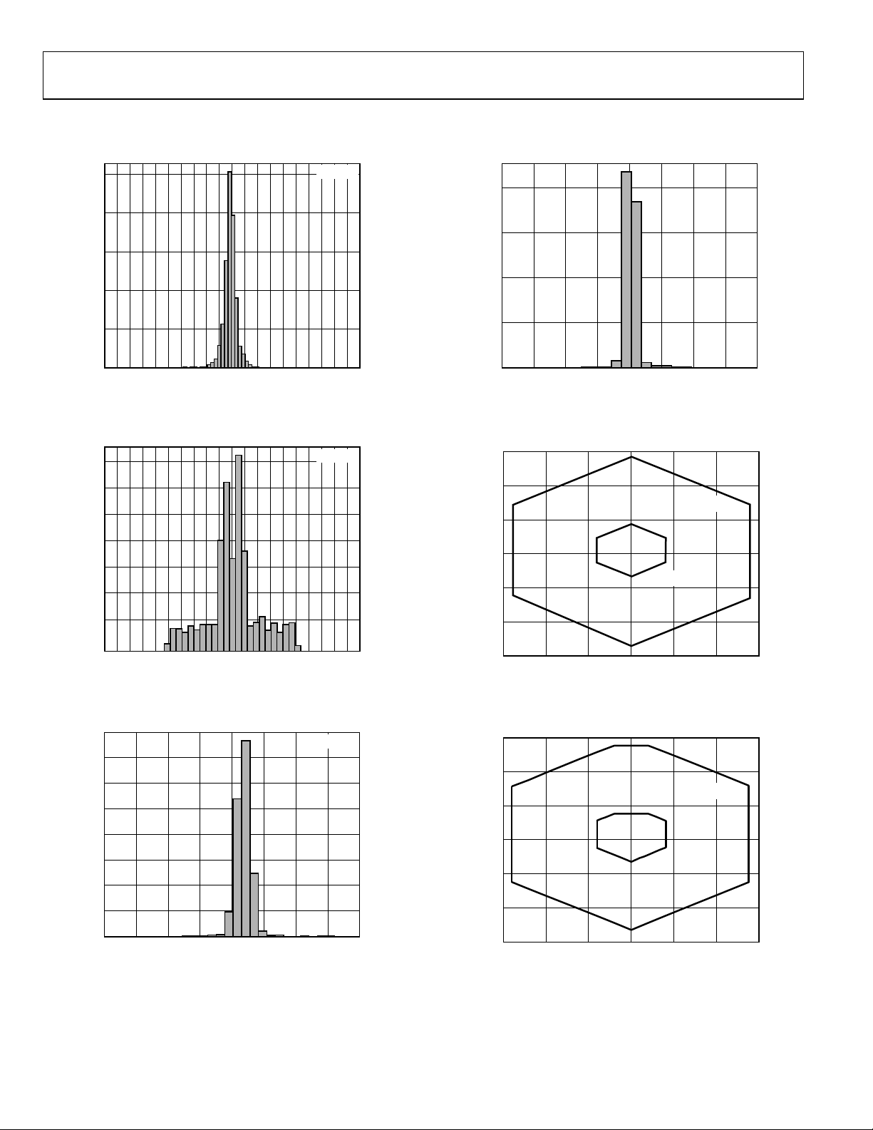
TYPICAL PERFORMANCE CHARACTERISTICS
500
400
300
N = 1713
800
600
200
NUMBER OF UNITS
100
0
–50 50403020100–10–20–30–40
CMRR (µV/V)
Figure 3. Typical Distribution for CMRR (G = 1)
300
250
200
150
NUMBER OF UNITS
100
10
0
–100 10080604020020406080
V
(µV)
OSI
Figure 4. Typical Distribution of Input Offset Voltage
700
600
500
N = 1713
N = 1713
400
NUMBER OF UNITS
200
0
–2.0 2.01. 51. 00.50–0.5–1.0–1.5
05947-003
I
OFFSET
(nA)
05947-006
Figure 6. Typical Distribution of Input Offset Current
15
10
= ±15V
V
VS = ±5V
S
05947-007
5
0
–5
–10
INPUT COMMON-MODE VOL TAGE (V)
–15
05947-004
–15 –10 –5 0 5 10 15
OUTPUT VOLTAGE (V)
Figure 7. Input Common-Mode Range vs. Output Voltage, G = 1
15
10
= ±15V
V
5
S
400
300
NUMBER OF UNITS
200
100
0
–2.0 2.01. 51. 00.50–0.5–1.0–1.5
I
BIAS
(nA)
Figure 5. Typical Distribution of Input Bias Current
05947-005
Rev. 0 | Page 8 of 24
0
–5
–10
INPUT COMMON-MODE VOL TAGE (V)
–15
–15 –10 –5 0 5 10 15
OUTPUT VOLTAGE (V)
VS = ±5V
Figure 8. Input Common-Mode Range vs. Output Voltage, G = 100
05947-008

AD8222
200
150
100
50
–50
–100
INPUT BIAS CURRENT (pA)
–150
–200
0
–15 151050–5–10
Figure 9. I
VS = ±15V
= ±5V
V
S
COMMON-MO DE VOLTAG E (V)
vs. Common-Mode Voltage
BIAS
2.0
1.8
1.6
1.4
1.2
1.0
0.8
0.6
0.4
0.2
CHANGE IN INPUT OFFSET VOLTAGE (µV)
0
024681
WARM-UP TIME (Minutes)
Figure 10. Change in Input Offset Voltage vs. Warm-Up Time
1000
800
600
400
200
0
–200
–400
INPUT BIAS CURRENT (pA)
–600
–800
–1000
–55 –35 –15 5 25 45 65 85 105 125
TEMPERATURE ( °C)
NEGATIVE
POSITIVE
OFFSET CURRENT
Figure 11. Input Bias Current and Offset Current vs. Temperature
05947-009
0
05947-010
05947-011
160
150
+PSRR (dB)
140
130
120
110
100
90
80
70
60
50
40
30
20
10
0
0.1 1M100k10k1k100101
GAIN = 100
GAIN = 10
FREQUENCY (Hz)
BANDWIDTH
GAIN = 1000
GAIN = 1
Figure 12. Positive PSRR vs. Frequency, RTI (G = 1 to 1000)
160
150
140
–PSRR (dB)
130
120
110
100
90
80
70
60
50
40
30
20
10
0
0.1 1M100k10k1k100101
FREQUENCY (Hz)
GAIN = 1000
GAIN = 100
GAIN = 10
GAIN = 1
Figure 13. Negative PSRR vs. Frequency, RTI (G = 1 to 1000)
10k
1k
GAIN = 1
TOTAL DRIFT: 25°C TO 85°C RTI (µV)
100
10
1
1 10M1M100k10k1k10010
GAIN = 10
GAIN = 100
GAIN = 1000
SOURCE RESIST ANCE (Ω)
Figure 14. Total Drift vs. Source Resistance
LIMITED
05947-012
05947-013
05947-014
Rev. 0 | Page 9 of 24

AD8222
VS–
VS–
70
GAIN = 1000
60
50
GAIN = 100
40
30
GAIN = 10
20
10
GAIN (dB)
GAIN = 1
0
–10
–20
–30
–40
100 1k 10k 100k 1M 10M
FREQUENCY (Hz)
Figure 15. Gain vs. Frequency
160
GAIN = 1000
150
GAIN = 100
140
130
GAIN = 10
CMRR (dB)
120
110
100
90
80
70
60
50
40
0.1 1M100k10k1k100101
GAIN = 1
FREQUENCY (Hz)
BANDWIDTH
LIMITED
Figure 16. CMRR vs. Frequency, RTI
160
GAIN = 1000
150
140
130
GAIN = 100
120
110
GAIN = 10
CMRR (dB)
100
90
80
70
60
50
40
0.1 1M100k10k1k100101
GAIN = 1
FREQUENCY (Hz)
BANDWIDTH
Figure 17. CMRR vs. Frequency, RTI, 1 kΩ Source Imbalance
LIMITED
05947-015
05947-016
05947-017
20
15
10
ΔCMR (µV/V)
5
0
–5
–10
–15
–20
–40 12010 0806040200–20
TEMPERATURE ( °C)
EXAMPLE PART 1
EXAMPLE PART 2
Figure 18. ΔCMR vs. Temperature, G = 1
+
0
–0.4
–0.8
–1.2
–1.6
–2.0
+2.0
+1.6
+1.2
INPUT VOLTAGE LIMIT (V)
+0.8
REFERRED TO SUPPLY VOLTAGES
+0.4
–VS+0
2 6 10 14 18
FROM +V
FROM –V
SUPPLY VOLTAGE (V)
Figure 19. Input Voltage Limit vs. Supply Voltage, G = 1
+
0
–0.4
–0.8
–1.2
–1.6
+1.6
+1.2
OUTPUT VOLTAGE SWING (V)
+0.8
REFERRED TO SUPPLY VOLTAGES
+0.4
+0
–V
S
2 6 10 14 18
= 10kΩ
R
L
RL = 10kΩ
SUPPLY VOLTAGE (V)
RL = 2kΩ
R
= 2kΩ
L
Figure 20. Output Voltage Swing vs. Supply Voltage, G = 1
05947-018
05947-019
05947-020
Rev. 0 | Page 10 of 24

AD8222
VS–
30
40
30
20
20
10
OUTPUT VOLTAGE SWING (V p-p)
0
1 10 100 1k 10k
LOAD RESIST ANCE (Ω)
05947-021
10
0
–10
–20
NONLINEARIT Y (10ppm/DIV)
–30
–40
–10–8–6–4–20246810
Figure 21. Output Voltage Swing vs. Load Resistance
+
0
–1
–2
–3
+3
+2
OUTPUT VO LTAGE SW ING (V)
REFERRED TO S UPPLY VOL TAGES
+1
+0
–V
S
01
OUTPUT CURRENT (mA)
SOURCING
SINKING
21110987654321
05947-022
Figure 22. Output Voltage Swing vs. Output Current, G = 1
1k
GAIN = 1
100
GAIN = 10
GAIN = 100
10
GAIN = 1000
VOLTAGE NOISE RTI (nV/ Hz)
1
110
Figure 25. Voltage Noise Spectral Density vs. Frequency (G = 1 to 1000)
4
2kΩ LOAD
600Ω LOAD
(V)
V
OUT
Figure 24. Gain Nonlinearity, G = 100
GAIN = 1000
BW LIMIT
100 1k 10k 100k
FREQUENCY (Hz)
10kΩ LOAD
05947-024
05947-026
3
2
1
10kΩ LOAD
0
–1
–2
NONLINEARIT Y (1ppm/DI V)
–3
–4
–10 –8 –6 –4 –2 0 2 4 6 8 10
600Ω LOAD
Figure 23. Gain Nonlinearity, G = 1
2kΩ LOAD
V
OUT
(V)
2µV/DIV 1s/DIV
05947-023
05947-027
Figure 26. 0.1 Hz to 10 Hz RTI Voltage Noise (G = 1)
Rev. 0 | Page 11 of 24

AD8222
30
GAIN = 10, 100, 1000
GAIN = 1
25
20
15
10
MAX OUTPUT VOLTAG E (V p-p)
5
0.1µV/DI V 1s/DIV
Figure 27. 0.1 Hz to 10 Hz RTI Voltage Noise (G = 1000)
1k
100
CURRENT NOISE (fA/ Hz)
10
1 10 100 1k 10k 100k
FREQUENCY (Hz)
Figure 28. Current Noise Spectral Density vs. Frequency
05947-028
0
1k 10k 100k 1M
FREQUENCY (Hz)
05947-031
Figure 30. Large Signal Frequency Response
5V/DIV
7.4µs TO 0. 01%
8.3µs TO 0.001%
0.002%/DIV
20µs/DIV
05947-029
05947-032
Figure 31. Large Signal Pulse Response and Settling Time (G = 1)
5V/DIV
5pA/DI V 1s/DIV
Figure 29. 0.1 Hz to 10 Hz Current Noise
05947-030
Rev. 0 | Page 12 of 24
4.8µs TO 0.01%
6.6µs TO 0.001%
0.002%/DIV
20µs/DIV
Figure 32. Large Signal Pulse Response and Settling G = 10)
05947-033

AD8222
5V/DIV
9.2µs TO 0. 01%
16.2µs TO 0.001%
0.002%/DIV
20µs/DIV
05947-034
Figure 33. Large Signal Pulse Response and Settling Time (G = 100)
5V/DIV
83µs TO 0.01%
112µs TO 0. 001%
0.002%/DIV
200µs/DIV
05947-035
Figure 34. Large Signal Pulse Response and Settling Time (G = 1000)
Figure 36. Small Signal Response, G = 10, R
Figure 37. Small Signal Response, G = 100, R
4µs/DIV20mV/DIV
= 2 kΩ, CL = 100 pF
L
10µs/DIV20mV/DIV
= 2 kΩ, CL = 100 pF
L
5947-037
5947-038
Figure 35. Small Signal Response, G = 1, R
4µs/DIV20mV/DIV
= 2 kΩ, CL = 100 pF
L
5947-036
Rev. 0 | Page 13 of 24
100µs/DIV20mV/DIV
5947-039
Figure 38. Small Signal Response, G = 1000, RL = 2 kΩ, CL = 100 pF

AD8222
15
10
SETTLED TO 0.001%
5
SETTLING TIME (µs)
SETTLED TO 0.01%
60
GAIN = 1000
40
GAIN = 100
20
GAIN = 10
GAIN (dB)
0
GAIN = 1
–20
0
0 5 10 15 20
OUTPUT VOLTAGE STEP SIZE (V)
Figure 39. Settling Time vs. Step Size (G = 1)
1k
100
10
SETTLING TIME (µs)
1
1 10 100
SETTLED TO 0.001%
SETTLED TO 0.01%
GAIN
Figure 40. Settling Time vs. Gain for a 10 V Step
200
180
160
140
SOURCE
= 20V p-p
V
OUT
GAIN = 1000
THERMAL CROSSTALK
VARIES WITH LOAD
SOURCE V
SMALLER TO
AVOID SLEW
RATE LIMI T
OUT
–40
100 10k1k 100k 1M 10M
05947-040
FREQUENCY (Hz)
05947-043
Figure 42. Differential Output Configuration: Gain vs. Frequency
100
CMR
90
80
70
LIMITED BY
MEASUREMENT
60
(dB)
OUT
CMR
1k
05947-041
SYSTEM
50
40
30
20
10
0
1 10k1k10010 100k 1M
FREQUENCY (Hz)
OUT
= 20 log
V
DIFF_OUT
V
CM_OUT
05947-056
Figure 43. Differential Output Configuration:
Common-Mode Output vs. Frequency
CHANNEL SEPARATIO N (dB)
120
100
80
60
11100k10k1k10010
FREQUENCY (Hz)
GAIN = 1
M
Figure 41. Channel Separation vs. Frequency, RL = 2 kΩ, Source Channel at G = 1
05947-042
Rev. 0 | Page 14 of 24

AD8222
THEORY OF OPERATION
II
V
B
A2A1
C1 C2
+V
S
400Ω 400Ω
–V
Q1
S
R1 24.7kΩ 24.7kΩ
+V
S
–V
S
R2
+V
S
R
G
–V
S
Figure 44. Simplified Schematic
AMPLIFIER ARCHITECTURE
The two instrumentation amplifiers of the AD8222 are based on
the classic three op amp topology.
schematic of one of the amplifiers. Input Transistors Q1 and Q2
are biased at a fixed current. Any differential input signal forces
the output voltages of A1 and A2 to change so that the differential
voltage also appears across R
R
must also flow through R1 and R2, resulting in a precisely
G
amplified version of the differential input signal between the
outputs of A1 and A2. Topologically, Q1, A1, and R1 and Q2,
A2, and R2 can be viewed as precision current feedback
amplifiers. The common-mode signal and the amplified
differential signal are applied to a difference amplifier that
rejects the common-mode voltage. The difference amplifier
employs innovations that result in low output offset voltage as
well as low output offset voltage drift.
Because the input amplifiers employ a current feedback
architecture, the gain-bandwidth product of the AD8222
increases with gain, resulting in a system that does not suffer
from the expected bandwidth loss of voltage feedback
architectures at higher gains.
The transfer function of the AD8222 is
V
OUT
= G(V
IN+
− V
IN−
) + V
Figure 44 shows a simplified
. The current that flows through
G
REF
COMPENSATIONIB COMPENSATI ON
I
Q2
B
10kΩ
10kΩ
+V
S
+IN–IN
–V
S
10kΩ
A3
10kΩ
+V
S
OUTPUT
+V
–V
S
S
REF
–V
S
05947-045
GAIN SELECTION
Placing a resistor across the RG terminals sets the gain of the
AD8222, which can be calculated by referring to
using the following gain equation.
R
G
k49.4
1
−=G
Table 8. Gains Achieved Using 1% Resistors
1% Standard Table Value of RG (Ω) Calculated Gain
49.9 k 1.990
12.4 k 4.984
5.49 k 9.998
2.61 k 19.93
1.00 k 50.40
499 100.0
249 199.4
100 495.0
49.9 991.0
The AD8222 defaults to G = 1 when no gain resistor is used.
The tolerance and gain drift of the R
resistor should be added
G
to the AD8222’s specifications to determine the total gain
accuracy of the system. When the gain resistor is not used,
gain error and gain drift are kept to a minimum.
Tabl e 8 or by
where
G
1 +=
k49.4
GR
Rev. 0 | Page 15 of 24

AD8222
REFERENCE TERMINAL
The output voltage of the AD8222 is developed with respect to
the potential on the reference terminal. This is useful when the
output signal needs to be offset to a precise midsupply level. For
example, a voltage source can be tied to the REF pin to levelshift the output so that the AD8222 can drive a single-supply
ADC. The REF pin is protected with ESD diodes and should
not exceed either +V
or −VS by more than 0.3 V.
S
For best performance, source impedance to the REF terminal
should be kept below 1 Ω. As shown in
Figure 44, the reference
terminal, REF, is at one end of a 10 k resistor. Additional
impedance at the REF terminal adds to this 10 k resistor and
results in amplification of the signal connected to the positive
input. The amplification from the additional R
can be
REF
computed by
( )
k102
REF
RR++k20
REF
Only the positive signal path is amplified; the negative path is
unaffected. This uneven amplification degrades the amplifier’s
CMRR.
INCORRECT
AD8222
V
REF
Figure 45. Driving the Reference Pin
V
REF
CORRECT
AD8222
+
OP2177
–
V
REF
CORRECT
AD8222
+
AD8222
–
LAYOUT
The AD8222 is a high precision device. To ensure optimum
performance at the PC board level, care must be taken in the
design of the board layout. The AD8222 pinout is arranged in a
logical manner to aid in this task.
Package Considerations
The AD8222 comes in a 4 mm × 4 mm LFCSP. Beware of
blindly copying the footprint from another 4 mm × 4 mm
LFCSP part; it may not have the same thermal pad size and
leads. Refer to the
the PCB symbol has the correct dimensions. Space between the
leads and thermal pad should be kept as wide as possible for the
best bias current performance.
Outline Dimensions section to verify that
05947-054
Thermal Pad
The AD8222’s 4 mm × 4 mm LFCSP comes with a thermal pad.
This pad is connected internally to −V
. The pad can either be
S
left unconnected or connected to the negative supply rail.
To preserve maximum pin compatibility with future dual
instrumentation amplifiers, leave the pad unconnected
. This
can be done by not soldering the paddle at all or by soldering
the part to a landing that is a not connected to any other net.
For high vibration applications, a landing is recommended.
Because the AD8222 dissipates little power, heat dissipation is
rarely an issue. If improved heat dissipation is desired (for example,
when driving heavy loads), connect the thermal pad to the
negative supply rail. For the best heat dissipation performance,
the negative supply rail should be a plane in the board. See
the section for thermal coefficients with and without the pad
soldered.
Common-Mode Rejection over Frequency
The AD8222 has a higher CMRR over frequency than typical
in-amps, which gives it greater immunity to disturbances, such
as line noise and its associated harmonics. A well-implemented
layout is required to maintain this high performance. Input
source impedances should be matched closely. Source resistance
should be placed close to the inputs so that it interacts with as
little parasitic capacitance as possible.
Parasitics at the RGx pins can also affect CMRR over frequency.
The PCB should be laid out so that the parasitic capacitances at
each pin match. Traces from the gain setting resistor to the RGx
pins should be kept short to minimize parasitic inductance.
Reference
Errors introduced at the reference terminal feed directly to the
output. Care should be taken to tie REF to the appropriate local
ground.
Power Supplies
A stable dc voltage should be used to power the instrumentation
amplifier. Noise on the supply pins can adversely affect
performance.
The AD8222 has two positive supply pins (Pin 5 and Pin 16)
and two negative supply pins (Pin 8 and Pin 13). While the part
functions with only one pin from each supply pair connected,
both pins should be connected for specified performance and
optimum reliability.
Rev. 0 | Page 16 of 24

AD8222
−
V
V
The AD8222 should be decoupled with 0.1 µF bypass capacitors,
one for each supply. The positive supply decoupling capacitor
should be placed near Pin 16, and the negative supply
decoupling capacitor should be placed near Pin 8. Each supply
should also be decoupled with a 10 µF tantalum capacitor. The
tantalum capacitor can be placed further away from the
AD8222 and can generally be shared by other precision integrated
circuits.
Figure 46 shows an example layout.
0.1µF
AD8222
1
R
G
2
3
4
5678
0.1µF
13141516
12
11
10
9
R
G
INCORRECT
+V
S
AD8222
–V
S
TRANSFORMER
+V
S
AD8222
–V
S
THERMOCOUPLE
+V
S
C
AD8222
C
CAPACITIVELY COUPLE D
REF
–V
S
Figure 47. Creating an I
REF
REF
f
HIGH-PASS
CORRECT
+V
AD8222
–V
TRANSFORMER
+V
AD8222
10MΩ
–V
THERMOCOUPL E
+V
C
R
1
=
2πRC
C
CAPACITIVELY COUPLE D
Path
BIAS
AD8222
R
–V
S
REF
S
S
REF
S
S
REF
S
5947-047
Figure 46. Example Layout
SOLDER WASH
The solder process can leave flux and other contaminants on
the board. When these contaminants are between the AD8222
leads and thermal pad, they can create leakage paths that are
larger than the AD8222’s bias currents. A thorough washing
process removes these contaminants and restores the AD8222’s
excellent bias current performance.
INPUT BIAS CURRENT RETURN PATH
The input bias current of the AD8222 must have a return path
to common. When the source, such as a thermocouple, cannot
provide a return current path, one should be created, as shown
in
Figure 47.
INPUT PROTECTION
05947-046
All terminals of the AD8222 are protected against ESD (1 kV—
human body model). In addition, the input structure allows for
dc overload conditions of about 2½ V beyond the supplies.
Input Voltages Beyond the Rails
For larger input voltages, an external resistor should be used in
series with each input to limit current during overload conditions.
The AD8222 can safely handle a continuous 6 mA current. The
limiting resistor can be computed from
R
LIMIT
SUPPLY
≥
mA6
−
400
IN
For applications where the AD8222 encounters extreme overload
voltages, such as cardiac defibrillators, external series resistors
and low leakage diode clamps, such as the BAV199L, the FJH1100s,
or the SP720, should be used.
Rev. 0 | Page 17 of 24

AD8222
V
Differential Input Voltages at High Gains
When operating at high gain, large differential input voltages
can cause more than 6 mA of current to flow into the inputs.
This condition occurs when the differential voltage exceeds
the following critical voltage
V
= (400 + RG) × (6 mA)
CRITICAL
This is true for differential voltages of either polarity.
The maximum allowed differential voltage can be increased by
adding an input protection resistor in series with each input.
The value of each protection resistor should be
R
PROTECT
= (V
DIFF_MAX
− V
CRITICAL
)/6 mA
RF INTERFERENCE
RF rectification is often a problem when amplifiers are used in
applications where there are strong RF signals. The disturbance
can appear as a small dc offset voltage. High frequency signals
can be filtered with a low-pass, RC network placed at the input
of the instrumentation amplifier, as shown in
filter limits the input signal bandwidth according to the
following relationship.
FilterFreq+π=
FilterFreqπ=
where C
≥ 10CC.
D
Diff
CM
1
1
RC
2
C
)(22
CD
CCR
Figure 48. The
+15
R
4.02kΩ
R
4.02kΩ
0.1µF
C
C
1nF
C
D
10nF
C
C
1nF
Figure 48. RFI Suppression
499Ω
R1
0.1µF
+IN
AD8222
–IN
–15V
REF
10µF
10µF
V
OUT
05947-048
Figure 48 shows an example where the differential filter
frequency is approximately 2 kHz, and the common-mode filter
frequency is approximately 40 kHz.
Values of R and C
Mismatch between the R × C
at negative input degrades the CMRR of the AD8222. By
R × C
C
using a value of C
should be chosen to minimize RFI.
C
at the positive input and the
C
10× larger than the value of CC, the effect of
D
the mismatch is reduced and performance is improved.
COMMON-MODE INPUT VOLTAGE RANGE
The three op amp architecture of the AD8222 applies gain and
then removes the common-mode voltage. Therefore, internal
nodes in the AD8222 experience a combination of both the
gained signal and the common-mode signal. This combined
signal can be limited by the voltage supplies even when the
individual input and output signals are not.
show the allowable common-mode input voltage ranges for
various output voltages, supply voltages, and gains.
Figure 7 and Figure 8
Rev. 0 | Page 18 of 24

AD8222
APPLICATIONS
DIFFERENTIAL OUTPUT
The differential configuration of the AD8222 has the same
excellent dc precision specifications as the single-ended output
configuration and is recommended for applications in the
frequency range of dc to 100 kHz.
The circuit configuration is shown in
output specification in
Tabl e 2 and Ta b le 4 refer to this
configuration only. The circuit includes an RC filter that maintains
the stability of the loop.
Figure 49. The differential
Setting the Common-Mode Voltage
The output common-mode voltage is set by the average of +IN2
and REF2. The transfer function is
V
CM_OUT
= (V
+OUT
+ V
−OUT
)/2 = (V
+IN2
+ V
REF2
)/2
+IN2 and REF2 have different properties that allow the
reference voltage to be easily set for a wide variety of applications.
+IN2 has high impedance but cannot swing to the supply rails
of the part. REF2 must be driven with a low impedance but can
go 300 mV beyond the supply rails.
The transfer function for the differential output is:
V
DIFF_OUT
= V
+OUT
− V
−OUT
= (V
+IN
− V
−IN
) × G
where
G
1 +=
k49.4
GR
+IN
+
R
AD8222
G
–IN
–
Figure 49. Differential Circuit Schematic
AD8222
REF2
–
+
+OUT
10kΩ
100pF
+IN2
–OUT
A common application sets the common-mode output voltage
to the midscale of a differential ADC. In this case, the ADC
reference voltage would be sent to the +IN2 terminal, and
ground would be connected to the REF2 terminal. This would
produce a common-mode output voltage of half the ADC
reference voltage.
2-Channel Differential Output Using a Dual Op Amp
Another differential output topology is shown in Figure 50.
Instead of a second in-amp, ½ of a dual OP2177 op amp creates
the inverted output. Because the OP2177 comes in an MSOP,
this configuration allows the creation of a dual channel,
precision differential output in-amp with little board area.
Errors from the op amp are common to both outputs and are
thus common mode. Errors from mismatched resistors also
05947-049
create a common-mode dc offset. Because these errors are
common mode, they will likely be rejected by the next device
in the signal chain.
+IN
+OUT
V
REF
–IN
AD8222
REF
4.99kΩ
+
4.99kΩ
Figure 50. Differential Output Using Op Amp
–
OP2177
–OUT
05947-053
Rev. 0 | Page 19 of 24

AD8222
V
V
+
+IN
–IN
0.1µF
100pF
NPO
1kΩ
5%
1000pF
1kΩ
100pF
NPO
5%
0.1µF10µF
+
10µF
+12
AD8222
(DIFF OUT)
+5V REF
–12V
+IN2
REF2
+OUT
–OUT
Figure 51. Driving a Differential ADC
DRIVING A DIFFERENTIAL INPUT ADC
The AD8222 can be configured in differential output mode
to drive a differential analog-to-digital converter.
illustrates several of the concepts.
First Antialiasing Filter
The 1 kΩ resistor, 1000 pF capacitor, and 100 pF capacitors in
front of the in-amp form a 76 kHz filter. This is the first of two
antialiasing filters in the circuit and helps to reduce the noise of
the system. The 100 pF capacitors protect against commonmode RFI signals. Note that they are 5% COG/NPO types.
These capacitors match well over time and temperature, which
keeps the system’s CMRR high over frequency.
Second Antialiasing Filter
A 1 kΩ resistor and 2200 pF capacitor are located between each
AD8222 output and ADC input. They create a 72 kHz low-pass
filter for another stage of antialiasing protection.
These four elements also help distortion performance. The
2200 pF capacitor provides charge to the switched capacitor
front end of the ADC, while the 1 kΩ resistor shields the
AD8222 from driving any sharp current changes. If the
application requires a lower frequency antialiasing filter and is
distortion sensitive, increase the value of the capacitor rather
than the resistor.
Figure 51
1kΩ
1kΩ
2200pF 2200pF
+5V
0.1µF
VDD
IN+
AD7688
IN–
GND REF
10µF
IN
GND
X5R
0.1µF
+5V REF
05947-051
V
OUT
+12V
0.1µF
V
ADR435
The 1 kΩ resistors can also protect an ADC from overvoltages.
Because the AD8222 runs on wider supply voltages than a
typical ADC, there is a possibility of overdriving the ADC. This
is not an issue with a PulSAR® converter, such as the AD7688.
Its input can handle a 130 mA overdrive, which is much higher
than the short-circuit limit of the AD8222. However, other
converters have less robust inputs and may need the added
protection.
Reference
The ADR435 supplies a reference voltage to both the ADC and
the AD8222. Because REF2 on the AD8222 is grounded, the
common-mode output voltage is precisely half the reference
voltage, exactly where it needs to be for the ADC.
PRECISION STRAIN GAUGE
The low offset and high CMRR over frequency of the
AD8222 make it an excellent candidate for both ac and dc
bridge measurements. As shown in
be connected to the inputs of the amplifier directly.
10µF 0.1µF
350Ω
350Ω
350Ω350Ω
Figure 52. Precision Strain Gauge
Figure 52, the bridge can
5
+IN
+
R
AD8222
G
–
–IN
2.5V
05947-050
Rev. 0 | Page 20 of 24

AD8222
DRIVING CABLING
All cables have a certain capacitance per unit length, which
varies widely with cable type. The capacitive load from the cable
may cause peaking in the AD8222’s output response. To reduce
the peaking, use a resistor between the AD8222 and the cable.
Because cable capacitance and desired output response vary
widely, this resistor is best determined empirically. A good
starting point is 50 Ω.
The AD8222 operates at a low enough frequency that
transmission line effects are rarely an issue; therefore, the
resistor need not match the characteristic impedance of
the cable.
AD8222
(DIFF OUT)
AD8222
(SINGLE OUT)
Figure 53. Driving a Cable
05947-052
Rev. 0 | Page 21 of 24

AD8222
C
OUTLINE DIMENSIONS
0.50
0.40
INDI
SEATING
PLANE
PIN 1
ATO R
1.00
0.85
0.80
12° MAX
4.00
BSC SQ
3.75
BSC SQ
TOP VIEW
0.80 MAX
0.65 TYP
0.05 MAX
0.30
0.23
0.18
COMPLIANTTOJEDEC STANDARDS MO-220-VGGC.
0.02 NOM
0.20 REF
0.60 MAX
12
0.65
9
BSC
1.95 BCS
COPLANARITY
0.08
13
EXPOSED
8
BOTTOM VIEW
Figure 54. 16-Lead Lead Frame Chip Scale Package [LFCSP_VQ]
4 mm × 4 mm Body, Very Thin Quad
(CP-16-13)
Dimensions are shown in millimeters
PAD
0.30
1
16
4
5
P
N
I
N
I
2.65
2.50 SQ
2.35
0.25 MIN
1
R
O
C
I
A
T
D
031006-A
ORDERING GUIDE
Model Temperature Range Product Description Package Option
AD8222ACPZ-R7
AD8222ACPZ-RL
AD8222ACPZ-WP
AD8222BCPZ-R7
AD8222BCPZ-RL
AD8222BCPZ-WP
AD8222-EVAL Evaluation Board
1
Z = Pb-free part.
1
1
1
1
1
1
−40°C to +85°C 16-Lead LFCSP_VQ CP-16-13
−40°C to +85°C 16-Lead LFCSP_VQ CP-16-13
−40°C to +85°C 16-Lead LFCSP_VQ CP-16-13
−40°C to +85°C 16-Lead LFCSP_VQ CP-16-13
−40°C to +85°C 16-Lead LFCSP_VQ CP-16-13
−40°C to +85°C 16-Lead LFCSP_VQ CP-16-13
Rev. 0 | Page 22 of 24

AD8222
NOTES
Rev. 0 | Page 23 of 24

AD8222
NOTES
©2006 Analog Devices, Inc. All rights reserved. Trademarks and
registered trademarks are the property of their respective owners.
D05947-0-7/06(0)
Rev. 0 | Page 24 of 24
 Loading...