

+
Precision Instrumentation Amplifier
FEATURES
Easy to use
Available in space-saving MSOP
Gain set with 1 external resistor (gain range 1 to 1000)
Wide power supply range: ±2.3 V to ±18 V
Temperature range for specified performance:
−40°C to +85°C
Operational up to 125°C
Excellent AC specifications
80 dB minimum CMRR to 10 kHz ( G = 1)
825 kHz, –3 dB bandwidth (G = 1)
2 V/μs slew rate
Low noise
8 nV/√Hz, @ 1 kHz, maximum input voltage noise
0.25 μV p-p input noise (0.1 Hz to 10 Hz)
High accuracy dc performance (AD8221BR)
90 dB minimum CMRR (G = 1)
25 μV maximum input offset voltage
0.3 μV/°C maximum input offset drift
0.4 nA maximum input bias current
APPLICATIONS
Weigh scales
Industrial process controls
Bridge amplifiers
Precision data acquisition systems
Medical instrumentation
Strain gages
Transducer interfaces
GENERAL DESCRIPTION
The AD8221 is a gain programmable, high performance
instrumentation amplifier that delivers the industry’s highest
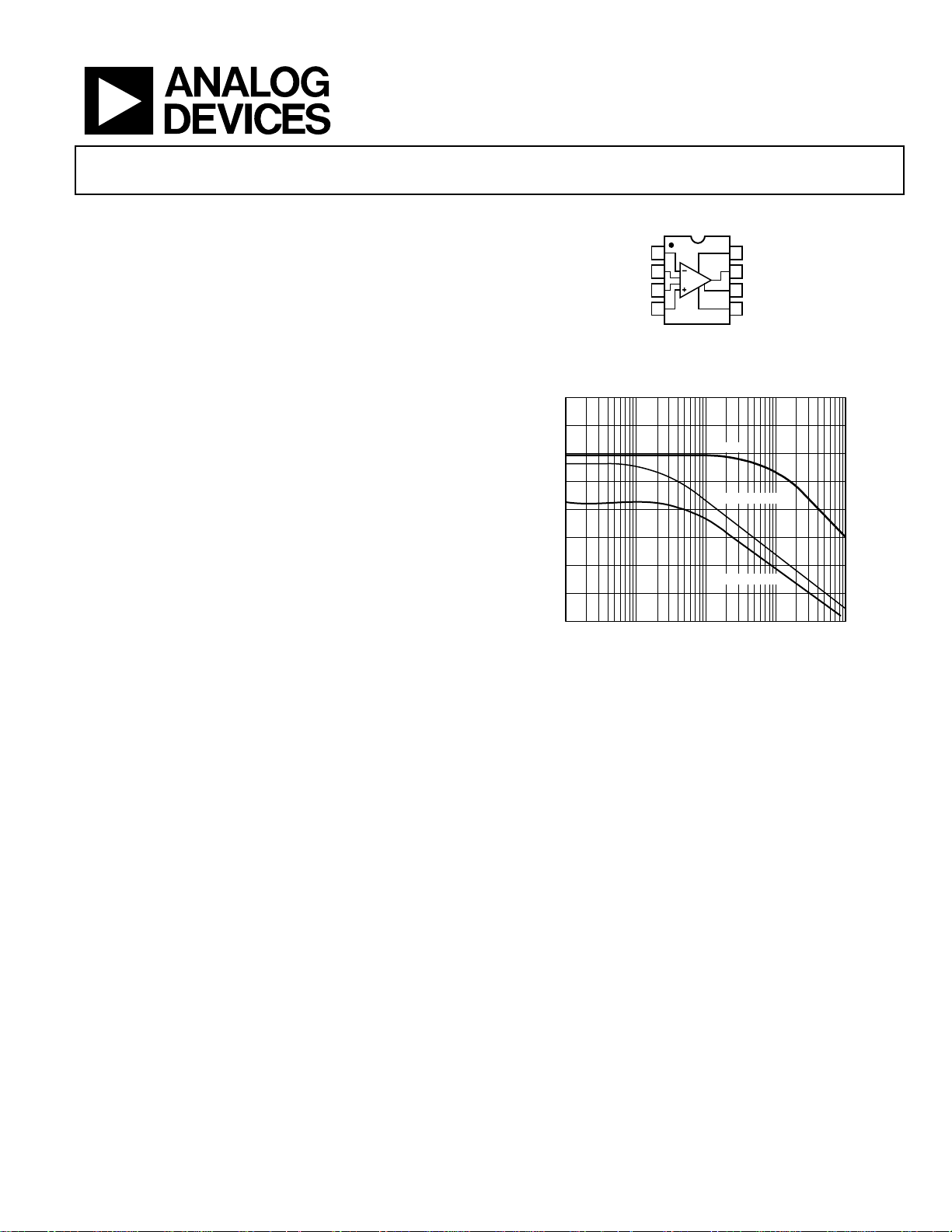
CMRR over frequency in its class. The CMRR of instrumentation
amplifiers on the market today falls off at 200 Hz. In contrast,
the AD8221 maintains a minimum CMRR of 80 dB to 10 kHz
for all grades at G = 1. High CMRR over frequency allows the
AD8221 to reject wideband interference and line harmonics,
greatly simplifying filter requirements. Possible applications
include precision data acquisition, biomedical analysis, and
aerospace instrumentation.
1
AD8221
CONNECTION DIAGRAM
1
–IN
2
R
G
3
R
G
4
IN
AD8221
TOP VIEW
Figure 1.
120
110
100
90
80
CMRR (dB)
70
60
50
40
10010 1k 10k 100k
FREQUENCY (Hz)
Figure 2. Typical CMRR vs. Frequency for G = 1
Low voltage offset, low offset drift, low gain drift, high gain
accuracy, and high CMRR make this part an excellent choice
in applications that demand the best dc performance possible,
such as bridge signal conditioning.
Programmable gain affords the user design flexibility. A single
resistor sets the gain from 1 to 1000. The AD8221 operates on
both single and dual supplies and is well suited for applications
where ±10 V input voltages are encountered.
The AD8221 is available in a low cost 8-lead SOIC and 8-lead
MSOP, both of which offer the industry’s best performance. The
MSOP requires half the board space of the SOIC, making it ideal
for multichannel or space-constrained applications.
Performance is specified over the entire industrial temperature
range of −40°C to +85°C for all grades. Furthermore, the AD8221
is operational from −40°C to +125°C
1
See Typical Performance Characteristics for expected operation from
85°C to 125°C.
8
+V
S
7
V
OUT
6
REF
5
–V
S
AD8221
COMPET ITOR 1
COMPET ITOR 2
1
.
03149-001
03149-002
Rev. B
Information furnished by Analog Devices is believed to be accurate and reliable. However, no
responsibility is assumed by Anal og Devices for its use, nor for any infringements of patents or ot her
rights of third parties that may result from its use. Specifications subject to change without notice. No
license is granted by implication or otherwise under any patent or patent rights of Analog Devices.
Trademarks and registered trademarks are the property of their respective owners.
One Technology Way, P.O. Box 9106, Norwood, MA 02062-9106, U.S.A.
Tel: 781.329.4700 www.analog.com
Fax: 781.461.3113 ©2003–2007 Analog Devices, Inc. All rights reserved.

AD8221
TABLE OF CONTENTS
Features .............................................................................................. 1
Applications....................................................................................... 1
General Description......................................................................... 1
Connection Diagram .......................................................................1
Revision History ............................................................................... 2
Specifications..................................................................................... 3
Absolute Maximum Ratings............................................................ 8
Thermal Characteristics .............................................................. 8
ESD Caution.................................................................................. 8
Typical Performance Characteristics............................................. 9
Theory of Operation ...................................................................... 16
Gain Selection............................................................................. 17
REVISION HISTORY
9/07—Rev. A to Rev. B
Changes to Features.......................................................................... 1
Changes to Table 1 Layout............................................................... 3
Changes to Table 2 Layout............................................................... 5
Changes to Figure 15...................................................................... 11
Changes to Figures 32.................................................................... 13
Changes to Figure 33, Figure 34, and Figure 35......................... 14
Updated Outline Dimensions....................................................... 21
Changes to Ordering Guide.......................................................... 22
11/03—Rev. 0 to Rev. A
Changes to Features.......................................................................... 1
Changes to Specifications Section.................................................. 4
Changes to Theory of Operation Section.................................... 13
Changes to Gain Selection Section............................................... 14
10/03—Revision 0: Initial Version
Layout ..........................................................................................17
Reference Terminal.................................................................... 18
Power Supply Regulation and Bypassing ................................ 18
Input Bias Current Return Path ............................................... 18
Input Protection ......................................................................... 18
RF Interference........................................................................... 19
Precision Strain Gage................................................................. 19
Conditioning ±10 V Signals for a +5 V Differential Input
ADC ............................................................................................. 19
AC-Coupled Instrumentation Amplifier................................ 20
Outline Dimensions .......................................................................21
Ordering Guide .......................................................................... 22
Rev. B | Page 2 of 24

AD8221
SPECIFICATIONS
VS = ±15 V, V
Table 1.
AR Grade BR Grade
Parameter Conditions Min Typ Max Min Typ Max Unit
COMMON-MODE REJECTION RATIO
CMRR DC to 60 Hz with 1 kΩ
Source Imbalance
G = 1 80 90 dB
G = 10 100 110 dB
G = 100 120 130 dB
G = 1000 130 140 dB
CMRR at 10 kHz VCM = −10 V to +10 V
G = 1 80 80 dB
G = 10 90 100 dB
G = 100 100 110 dB
G = 1000 100 110 dB
NOISE
Voltage Noise, 1 kHz
Input Voltage Noise, e
Output Voltage Noise, e
RTI f = 0.1 Hz to 10 Hz
G = 1 2 2 μV p-p
G = 10 0.5 0.5 μV p-p
G = 100 to 1000 0.25 0.25 μV p-p
Current Noise f = 1 kHz 40 40 fA/√Hz
f = 0.1 Hz to 10 Hz 6 6 pA p-p
VOLTAGE OFFSET
Input Offset, V
Over Temperature T = −40°C to +85°C 86 45 μV
Average TC 0.4 0.3 μV/°C
Output Offset, V
Over Temperature T = −40°C to +85°C 0.66 0.45 mV
Average TC 6 5 μV/°C
Offset RTI vs. Supply (PSR) VS = ±2.3 V to ±18 V
G = 1 90 110 94 110 dB
G = 10 110 120 114 130 dB
G = 100 124 130 130 140 dB
G = 1000 130 140 140 150 dB
INPUT CURRENT
Input Bias Current 0.5 1.5 0.2 0.4 nA
Over Temperature T = −40°C to +85°C 2.0 1 nA
Average TC 1 1 pA/°C
Input Offset Current 0.2 0.6 0.1 0.4 nA
Over Temperature T = −40°C to +85°C 0.8 0.6 nA
Average TC 1 1 pA/°C
REFERENCE INPUT
R
IN
I
IN
Voltage Range –V
Gain to Output 1 ± 0.0001 1 ± 0.0001 V/V
= 0 V, TA = 25°C, G = 1, RL = 2 kΩ, unless otherwise noted.
REF
= −10 V to +10 V
V
CM
RTI noise =
2
√
e
+ (eNO/G)
NI
V
NI
NO
1
OSI
OSO
, V
IN+
IN−
75 75 nV/√Hz
VS = ±5 V to ±15 V 60 25 μV
VS = ±5 V to ±15 V 300 200 μV
2
, V
= 0 8 8 nV/√Hz
REF
20 20 kΩ
V
, V
, V
IN+
= 0 50 60 50 60 μA
IN−
REF
S
+V
S
–V
S
+V
S
V
Rev. B | Page 3 of 24

AD8221
AR Grade BR Grade
Parameter Conditions Min Typ Max Min Typ Max Unit
POWER SUPPLY
Operating Range VS = ±2.3 V to ±18 V ±2.3 ±18 ±2.3 ±18 V
Quiescent Current 0.9 1 0.9 1 mA
Over Temperature T = −40°C to +85°C 1 1.2 1 1.2 mA
DYNAMIC RESPONSE
Small Signal −3 dB Bandwidth
G = 1 825 825 kHz
G = 10 562 562 kHz
G = 100 100 100 kHz
G = 1000 14.7 14.7 kHz
Settling Time 0.01% 10 V step
G = 1 to 100 10 10 μs
G = 1000 80 80 μs
Settling Time 0.001% 10 V step
G = 1 to 100 13 13 μs
G = 1000 110 110 μs
Slew Rate G = 1 1.5 2 1.5 2 V/μs
G = 5 to 100 2 2.5 2 2.5 V/μs
GAIN G = 1 + (49.4 kΩ/RG)
Gain Range 1 1000 1 1000 V/V
Gain Error V
G = 1 0.03 0.02 %
G = 10 0.3 0.15 %
G = 100 0.3 0.15 %
G = 1000 0.3 0.15 %
Gain Nonlinearity V
G = 1 to 10 RL = 10 kΩ 3 10 3 10 ppm
G = 100 RL = 10 kΩ 5 15 5 15 ppm
G = 1000 RL = 10 kΩ 10 40 10 40 ppm
G = 1 to 100 RL = 2 kΩ 10 95 10 95 ppm
Gain vs. Temperature
G = 1 3 10 2 5 ppm/°C
2
G > 1
INPUT
Input Impedance
Differential 100||2 100||2 GΩ||pF
Common Mode 100||2 100||2 GΩ||pF
Input Operating Voltage Range
3
Over Temperature T = −40°C to +85°C –VS + 2.0 +VS − 1.2 –VS + 2.0 +VS − 1.2 V
Input Operating Voltage Range VS = ±5 V to ±18 V –VS + 1.9 +VS − 1.2 –VS + 1.9 +VS − 1.2 V
Over Temperature T =−40°C to +85°C –VS + 2.0 +VS − 1.2 –VS + 2.0 +VS − 1.2 V
OUTPUT RL = 10 kΩ
Output Swing VS = ±2.3 V to ±5 V –VS + 1.1 +VS − 1.2 –VS + 1.1 +VS − 1.2 V
Over Temperature T = −40°C to +85°C –VS + 1.4 +Vs − 1.3 –VS + 1.4 +VS − 1.3 V
Output Swing VS = ±5 V to ±18 V –VS + 1.2 +VS − 1.4 –VS + 1.2 +VS − 1.4 V
Over Temperature T = –40°C to +85°C –VS + 1.6 +VS − 1.5 –VS + 1.6 +VS − 1.5 V
Short-Circuit Current 18 18 mA
± 10 V
OUT
= −10 V to +10 V
OUT
–50 –50 ppm/°C
VS = ±2.3 V to ±5 V –VS + 1.9 +VS − 1.1 –VS + 1.9 +VS − 1.1 V
Rev. B | Page 4 of 24

AD8221
AR Grade BR Grade
Parameter Conditions Min Typ Max Min Typ Max Unit
TEMPERATURE RANGE
Specified Performance –40 +85 –40 +85 °C
Operating Range
1
Total RTI VOS = (V
2
Does not include the effects of external resistor RG.
3
One input grounded. G = 1.
4
See Typical Performance Characteristics for expected operation between 85°C to 125°C.
Table 2.
Parameter Conditions
COMMON-MODE REJECTION RATIO (CMRR)
CMRR DC to 60 Hz with 1 kΩ Source Imbalance VCM = −10 V to +10 V
G = 1 80 dB
G = 10 100 dB
G = 100 120 dB
G = 1000 130 dB
CMRR at 10 kHz VCM = –10 V to +10 V
G = 1 80 dB
G = 10 90 dB
G = 100 100 dB
G = 1000 100 dB
NOISE
Voltage Noise, 1 kHz
Input Voltage Noise, e
Output Voltage Noise, e
RTI f = 0.1 Hz to 10 Hz
G = 1 2 μV p-p
G = 10 0.5 μV p-p
G = 100 to 1000 0.25 μV p-p
Current Noise f = 1 kHz 40 fA/√Hz
f = 0.1 Hz to 10 Hz 6 pA p-p
VOLTAGE OFFSET
Input Offset, V
Over Temperature T = −40°C to +85°C 135 μV
Average TC 0.9 μV/°C
Output Offset, V
Over Temperature T = −40°C to +85°C 1.00 mV
Average TC 9 μV/°C
Offset RTI vs. Supply (PSR) VS = ±2.3 V to ±18 V
G = 1 90 100 dB
G = 10 100 120 dB
G = 100 120 140 dB
G = 1000 120 140 dB
INPUT CURRENT
Input Bias Current 0.5 2 nA
Over Temperature T = −40°C to +85°C 3 nA
Average TC 3 pA/°C
Input Offset Current 0.3 1 nA
Over Temperature T = −40°C to +85°C 1.5 nA
Average TC 3 pA/°C
OSI
) + (V
1
OSI
OSO
4
/G).
OSO
–40 +125 –40 +125 °C
ARM Grade
Min Typ Max
RTI noise = √
V
NI
NO
, V
IN+
IN−
75 nV/√Hz
2
e
+ (eNO/G)
NI
, V
= 0 8 nV/√Hz
REF
2
Unit
VS = ±5 V to ±15 V 70 μV
VS = ±5 V to ±15 V 600 μV
Rev. B | Page 5 of 24

AD8221
ARM Grade
Parameter Conditions
Min Typ Max
REFERENCE INPUT
R
IN
I
IN
Voltage Range −V
20 kΩ
V
, V
, V
IN+
= 0 50 60 μA
IN−
REF
S
+V
S
Gain to Output 1 ± 0.0001 V/V
POWER SUPPLY
Operating Range VS = ±2.3 V to ±18 V ±2.3 ±18 V
Quiescent Current 0.9 1 mA
Over Temperature T = −40°C to +85°C 1 1.2 mA
DYNAMIC RESPONSE
Small Signal –3 dB Bandwidth
G = 1 825 kHz
G = 10 562 kHz
G = 100 100 kHz
G = 1000 14.7 kHz
Settling Time 0.01% 10 V step
G = 1 to 100 10 μs
G = 1000 80 μs
Settling Time 0.001% 10 V step
G = 1 to 100 13 μs
G = 1000 110 μs
Slew Rate G = 1 1.5 2 V/μs
G = 5 to 100 2 2.5 V/μs
GAIN G = 1 + (49.4 kΩ/RG)
Gain Range 1 1000 V/V
Gain Error V
± 10 V
OUT
G = 1 0.1 %
G = 10 0.3 %
G = 100 0.3 %
G = 1000 0.3 %
Gain Nonlinearity V
= −10 V to +10 V
OUT
G = 1 to 10 RL = 10 kΩ 5 15 ppm
G = 100 RL = 10 kΩ 7 20 ppm
G = 1000 RL = 10 kΩ 10 50 ppm
G = 1 to 100 RL = 2 kΩ 15 100 ppm
Gain vs. Temperature
G = 1 3 10 ppm/°C
2
G > 1
–50 ppm/°C
INPUT
Input Impedance
Differential 100||2 GΩ/pF
Common Mode 100||2 GΩ/pF
Input Operating Voltage Range
3
VS = ±2.3 V to ±5 V –VS + 1.9 +VS − 1.1 V
Over Temperature T = −40°C to +85°C –VS + 2.0 +VS − 1.2 V
Input Operating Voltage Range VS = ±5 V to ±18 V –VS + 1.9 +VS − 1.2 V
Over Temperature T = −40°C to +85°C –VS + 2.0 +VS − 1.2 V
OUTPUT RL = 10 kΩ
Output Swing VS = ±2.3 V to ±5 V –VS + 1.1 +VS − 1.2 V
Over Temperature T = −40°C to +85°C –VS + 1.4 +VS − 1.3 V
Output Swing VS = ±5 V to ±18 V –VS + 1.2 +VS − 1.4 V
Over Temperature T = −40°C to +85°C –VS + 1.6 +VS − 1.5 V
Short-Circuit Current 18 mA
Unit
V
Rev. B | Page 6 of 24

AD8221
ARM Grade
Parameter Conditions
Min Typ Max
TEMPERATURE RANGE
Specified Performance −40 +85 °C
OSI
) + (V
4
/G).
OSO
−40 +125 °C
Operating Range
1
Total RTI VOS = (V
2
Does not include the effects of external resistor RG.
3
One input grounded. G = 1.
4
See Typical Performance Characteristics for expected operation between 85°C to 125°C.
Unit
Rev. B | Page 7 of 24
AD8221
ABSOLUTE MAXIMUM RATINGS
Table 3.
Parameter Rating
Supply Voltage ±18 V
Internal Power Dissipation 200 mW
Output Short-Circuit Current Indefinite
Input Voltage (Common-Mode) ±V
Differential Input Voltage ±V
Storage Temperature Range −65°C to +150°C
Operating Temperature Range
1
Temperature range for specified performance is –40°C to +85°C. See Typical
Performance Characteristics for expected operation from 85°C to 125°C.
1
S
S
−40°C to +125°C
Stresses above those listed under Absolute Maximum Ratings
may cause permanent damage to the device. This is a stress
rating only; functional operation of the device at these or any
other conditions above those indicated in the operational
section of this specification is not implied. Exposure to absolute
maximum rating conditions for extended periods may affect
device reliability.
THERMAL CHARACTERISTICS
Specification for a device in free air.
Table 4.
Package θ
8-Lead SOIC, 4-Layer JEDEC Board 121 °C/W
8-Lead MSOP, 4-Layer JEDEC Board 135 °C/W
Unit
JA
ESD CAUTION
Rev. B | Page 8 of 24

AD8221
TYPICAL PERFORMANCE CHARACTERISTICS
T = 25°C, VS = ±15 V, RL = 10 kΩ, unless otherwise noted.
1600
3500
1400
1200
1000
UNITS
2400
2100
1800
1500
1200
UNITS
800
600
400
200
0
0–50–100–150 50 100 150
CMR (µV/V)
Figure 3. Typical Distribution for CMR (G = 1)
900
600
300
3000
2500
2000
UNITS
1500
1000
500
0
03149-003
INPUT OFFSET CURRENT ( nA)
0–0.3–0.6–0.9 0.3 0.6 0.9
03149-006
Figure 6. Typical Distribution of Input Offset Current
15
10
VS = ±15V
5
0
–5
–10
INPUT COMMON-MODE VOLTAGE (V)
VS = ±5V
0
INPUT OFFSET VOLTAGE (µV)
0–20–40–60 20 40 60
03149-004
Figure 4. Typical Distribution of Input Offset Voltage
3000
2500
2000
1500
UNITS
1000
500
0
INPUT BIAS CURRENT (nA)
0–0.5–1.0–1.5 0.5 1.0 1. 5
03149-005
Figure 5. Typical Distribution of Input Bias Current
–15
–5 0–15 –10 5 10 15
OU T PU T V OLTAGE (V )
Figure 7. Input Common-Mode Range vs. Output Voltage, G = 1
15
10
VS = ±15V
5
0
–5
–10
INPUT COMMON-MODE VOLTAGE (V)
–15
–5 0–15 –10 5 10 15
OUTPUT VOLTAGE (V)
VS = ±5V
Figure 8. Input Common-Mode Range vs. Output Voltage, G = 100
03149-007
03149-008
Rev. B | Page 9 of 24

AD8221
T
A
0.80
180
0.75
0.70
0.65
0.60
0.55
0.50
INPUT BIAS CURRENT (nA)
0.45
0.40
VS = ±15V
VS = ±5V
–5 0–15 –10 5 10 15
COMMON-MODE VOLTAGE (V)
Figure 9. I
BIAS
vs. CMV
2.00
1.75
AGE (µV)
1.50
1.25
1.00
0.75
0.50
0.25
CHANGE IN INPUT OFFSET VOL
0
0.10.01 1 10
WARM-UP TIME (min)
Figure 10. Change in Input Offset Voltage vs. Warm-Up Time
5
VS = ±15V
4
3
2
1
INPUT OFFSET CURRENT
0
–1
INPUT CURRENT (n A)
–2
–3
–4
–5
–40 –20 0 20 40 60 80 100 120 140
INPUT BIAS CURRENT
TEMPERATURE (° C)
Figure 11. Input Bias Current and Offset Current vs. Temperature
160
GAIN = 1000
140
GAIN = 100
120
GAIN = 10
100
GAIN = 1
80
POSITIVE PSRR (dB)
60
40
20
0.1 1 10 100 1k 10k 100k 1M
03149-009
FREQUENCY ( Hz)
GAIN = 1000
03149-012
Figure 12. Positive PSRR vs. Frequency, RTI (G = 1 to 1000)
180
160
GAIN = 1000
140
GAIN = 100
120
GAIN = 10
100
GAIN = 1
TIVE PSRR (dB)
80
NEG
60
40
20
0.1 1 10 100 1k 10k 100k 1M
03149-010
FREQUENCY ( Hz)
03149-013
Figure 13. Negative PSRR vs. Frequency, RTI (G = 1 to 1000)
100k
10k
BEST AVAILABLE FET
INPUT IN-AMP GAIN = 1
1k
100
TOTAL DRIFT 25°C – 85° C RTI (µ V)
10
03149-011
BEST AVAI LABLE FE T
INPUT IN-AMP GAIN = 1000
AD8221 GAIN = 1
AD8221 GAIN = 1000
1k 10k10 100 100k 1M 10M
SOURCE RESIS TANCE (Ω)
03149-014
Figure 14. Total Drift vs. Source Resistance
Rev. B | Page 10 of 24

AD8221
V
T
VS–
70
GAIN = 1000
60
50
GAIN = 100
40
30
GAIN = 10
20
GAIN (dB)
10
GAIN = 1
0
–10
–20
–30
100 1k 10k 100k 1M 10M
FREQUENCY (Hz)
Figure 15. Gain vs. Frequency
160
GAIN = 1000
140
GAIN = 100
120
GAIN = 10
100
GAIN = 1
CMRR (dB)
80
60
40
0.1 1 10 100 1k 10k 100k 1M
FREQUENCY ( Hz)
Figure 16. CMRR vs. Frequency, RTI
160
GAIN = 1000
GAIN = 100
140
GAIN = 10
120
GAIN = 1
100
CMRR (dB)
80
60
40
0.1 1 10 100 1k 10k 100k 1M
FREQUENCY (Hz)
Figure 17. CMRR vs. Frequency, RTI, 1 kΩ Source Imbalance
03149-015
03149-016
03149-017
100
80
60
40
20
0
CMR (µV/V)
–20
–40
–60
–80
–100
–40 –20 0 20 40 60 80 100 120 140
TEMPERATURE (°C)
Figure 18. CMR vs. Temperature
+
–0
S
–0.4
–0.8
–1.2
–1.6
–2.0
–2.4
AGE LIMIT (V)
+2.4
+2.0
+1.6
INPUT VOL
+1.2
REFERRED TO SUPPLY VOLTAGES
+0.8
+0.4
–VS +0
50 101520
SUPPLY VOLTAGE (±V)
Figure 19. Input Voltage Limit vs. Supply Voltage, G = 1
+
0
–0.4
–0.8
–1.2
–1.6
–2.0
+2.0
+1.6
+1.2
OUTPUT VOLTAGE SWING (V)
+0.8
REFERRED TO SUPPLY VOLTAGES
+0.4
–VS +0
501015
SUPPLY VOLTAGE (±V)
Figure 20. Output Voltage Swing vs. Supply Voltage, G = 1
RL = 10kΩ
RL = 2kΩ
RL = 2kΩ
RL = 10kΩ
03149-018
03149-019
20
03149-020
Rev. B | Page 11 of 24

AD8221
V
30
20
VS = ±15V
VS = ±15V
10
OUTPUT VOLTAGE SWING (V p-p)
0
101 100 1k 10k
LOAD RESISTANCE (Ω)
Figure 21. Output Voltage Swing vs. Load Resistance
–0
+
S
–1
–2
–3
+3
+2
OUTPUT VOLTAGE SWING (V)
REFERRED TO SUPPLY VOLTAGES
+1
–VS +0
0123456789101112
OUTPUT CURRENT (mA)
SOURCING
SINKING
Figure 22. Output Voltage Swing vs. Output Current, G = 1
V
S
= ±15V
ERROR (10ppm/ DIV)
–10 –8 –6 –4 –2 0 2 4 6 8 10
03149-021
Figure 24. Gain Nonlinearity, G = 100, R
OUTPUT VOLTAGE (V)
= 10 kΩ
L
03149-024
VS = ±15V
ERROR (100pp m/DIV)
–10 –8 –6 –4 –2 0 2 4 6 8 10
03149-022
Figure 25. Gain Nonlinearity, G = 1000, R
OUTPUT VOLTAGE (V)
= 10 kΩ
L
03149-025
1k
GAIN = 1
100
GAIN = 10
GAIN = 100
ERROR (1ppm/ DIV)
–10–8–6–4–20246810
Figure 23. Gain Nonlinearity, G = 1, R
OUTPUT VOLTAGE (V)
= 10 kΩ
L
03149-023
10
GAIN = 1000
VOLTAGE NOISE RTI (nV/ Hz)
1
1 10 100 1k 10k 100k
FREQUENCY (Hz)
GAIN = 1000
BW LIMIT
Figure 26. Voltage Noise Spectral Density vs. Frequency (G = 1 to 1000)
03149-026
Rev. B | Page 12 of 24

AD8221
T
Figure 27. 0.1 Hz to 10 Hz RTI Voltage Noise (G = 1)
Figure 28. 0.1 Hz to 10 Hz RTI Voltage Noise (G = 1000)
1k
1s/DIV2µV/DIV
03149-027
1s/DIV5pA/DIV
03149-030
Figure 30. 0.1 Hz to 10 Hz Current Noise
30
25
20
AGE (V p-p)
15
10
OUTPUT VOL
5
0
1s/DIV0. 1µV/DIV
3149-028
1k 100k10k 1M
GAIN = 1 G AIN = 10, 100, 1000
FREQUENCY (Hz)
VS = ±15V
03149-031
Figure 31. Large Signal Frequency Response
5V/DIV
100
CURRENT NOISE ( fA/ Hz)
10
101 100 1k 10k
FREQUENCY (Hz)
Figure 29. Current Noise Spectral Density vs. Frequency
0.002%/DIV
03149-029
Figure 32. Large Signal Pulse Response and Settling Time (G = 1), 0.002%/DIV
7.9µs TO 0.01%
8.5µs TO 0. 001%
20µs/DIV
03149-032
Rev. B | Page 13 of 24

AD8221
5V/DIV
4.9µs TO 0. 01%
0.002%/DIV
5.6µs TO 0. 001%
20mV/DIV
20µs/DIV
Figure 33. Large Signal Pulse Response and Settling Time (G = 10),
0.002%/DIV
5V/DIV
0.002%/DIV
10.3µs TO 0.01%
13.4µs TO 0.001%
20µs/DIV
Figure 34. Large Signal Pulse Response and Settling Time (G = 100),
0.002%/DIV
03149-033
Figure 36. Small Signal Response, G = 1, R
L
4µs/DIV
= 2 kΩ, CL = 100 pF
03149-036
20mV/DIV
03149-034
Figure 37. Small Signal Response, G = 10, R
4µs/DIV
= 2 kΩ, CL = 100 pF
L
03149-037
5V/DIV
0.002%/DIV
83µs TO 0. 01%
112µs TO 0.001%
200µs/DI V
Figure 35. Large Signal Pulse Response and Settling Time (G = 1000),
0.002%/DIV
03149-035
Rev. B | Page 14 of 24
20mV/DIV
Figure 38. Small Signal Response, G = 100, R
10µs/DIV
= 2 kΩ, CL = 100 pF
L
3149-038

AD8221
1000
100
2
SETTL ED TO 0.001%
SETTLED TO 0.01%
GAIN
03149-041
20mV/DIV
100µs/DI V
10
SETTLING TIME (µs)
1
03149-039
1 10010 1000
Figure 39. Small Signal Response, G = 1000, R
15
10
SETTLED TO 0.001%
5
SETTLING TIME (µs)
0
SETTLED TO 0.01%
501015
OUTPUT VOLTAGE STEP SIZE (V)
Figure 40. Settling Time vs. Step Size (G = 1)
= 2 kΩ, CL = 100 pF
L
Figure 41. Settling Time vs. Gain for a 10 V Step
20
03149-040
Rev. B | Page 15 of 24

AD8221
+
THEORY OF OPERATION
II
C1 C2
+V
S
400Ω 400Ω
–V
Q1
S
R1 24.7kΩ 24.7kΩ
+V
–V
V
B
R2
+V
S
R
S
S
G
–V
S
Figure 42. Simplified Schematic
The AD8221 is a monolithic instrumentation amplifier based
on the classic 3-op amp topology. Input transistors Q1 and Q2
are biased at a fixed current so that any differential input signal
forces the output voltages of A1 and A2 to change accordingly.
A signal applied to the input creates a current through R
, R1,
G
and R2, such that the outputs of A1 and A2 deliver the correct
voltage. Topologically, Q1, A1, R1 and Q2, A2, R2 can be
viewed as precision current feedback amplifiers. The amplified
differential and common-mode signals are applied to a
difference amplifier that rejects the common-mode voltage
but amplifies the differential voltage. The difference amplifier
employs innovations that result in low output offset voltage as
well as low output offset voltage drift. Laser-trimmed resistors
allow for a highly accurate in-amp with gain error typically less
than 20 ppm and CMRR that exceeds 90 dB (G = 1).
compensation
Using superbeta input transistors and an I
B
B
scheme, the AD8221 offers extremely high input impedance,
low I
B, low I
B
drift, low IB
B
, low input bias current noise, and
OS
extremely low voltage noise of 8 nV/√Hz.
The transfer function of the AD8221 is
G
1+=
k4.49
GR
Users can easily and accurately set the gain using a single
standard resistor.
A2A1
Q2
I
COMPENSATIONIB COMPENSATION
B
10kΩ
10kΩ
+V
S
+IN–IN
–V
S
10kΩ
10kΩ
A3
+V
S
OUTPUT
+V
–V
S
S
REF
–V
S
03149-042
Because the input amplifiers employ a current feedback
architecture, the gain-bandwidth product of the AD8221
increases with gain, resulting in a system that does not suffer
from the expected bandwidth loss of voltage feedback
architectures at higher gains.
To maintain precision even at low input levels, special attention
was given to the design and layout of the AD8221, resulting in
an in-amp whose performance satisfies the most demanding
applications.
A unique pinout enables the AD8221 to meet a CMRR
specification of 80 dB at 10 kHz (G = 1) and 110 dB at 1 kHz
(G = 1000). The balanced pinout, shown in
Figure 43, reduces
the parasitics that had, in the past, adversely affected CMRR
performance. In addition, the new pinout simplifies board
layout because associated traces are grouped together. For
example, the gain setting resistor pins are adjacent to the
inputs, and the reference pin is next to the output.
1
–IN
2
R
G
3
R
G
4
IN
AD8221
TOP VIEW
Figure 43. Pinout Diagram
8
+V
S
7
V
OUT
6
REF
5
–V
S
03149-043
Rev. B | Page 16 of 24

AD8221
GAIN SELECTION
Placing a resistor across the RG terminals set the gain of
AD8221, which can be calculated by referring to
by using the gain equation.
G
R
k4.49
1
−=G
Table 5. Gains Achieved Using 1% Resistors
1% Standard Table Value of RG (Ω) Calculated Gain
49.9 k 1.990
12.4 k 4.984
5.49 k 9.998
2.61 k 19.93
1.00 k 50.40
499 100.0
249 199.4
100 495.0
49.9 991.0
The AD8221 defaults to G = 1 when no gain resistor is used.
Gain accuracy is determined by the absolute tolerance of R
The TC of the external gain resistor increases the gain drift of
the instrumentation amplifier. Gain error and gain drift are kept
to a minimum when the gain resistor is not used.
Table 5 or
.
G
Grounding
The output voltage of the AD8221 is developed with respect to
the potential on the reference terminal. Care should be taken to
tie REF to the appropriate local ground.
In mixed-signal environments, low level analog signals need to
be isolated from the noisy digital environment. Many ADCs
have separate analog and digital ground pins. Although it is
convenient to tie both grounds to a single ground plane, the
current traveling through the ground wires and PC board may
cause hundreds of millivolts of error. Therefore, separate analog
and digital ground returns should be used to minimize the
current flow from sensitive points to the system ground. An
example layout is shown in
Figure 44 and Figure 45.
LAYOUT
Careful board layout maximizes system performance. Traces
from the gain setting resistor to the R
short as possible to minimize parasitic inductance. To ensure
the most accurate output, the trace from the REF pin should
either be connected to the local ground of the AD8221, as shown
Figure 46, or connected to a voltage that is referenced to the
in
local ground of the AD8221.
Common-Mode Rejection
One benefit of the high CMRR over frequency of the AD8221 is
that it has greater immunity to disturbances, such as line noise
and its associated harmonics, than do typical instrumentation
amplifiers. Typically, these amplifiers have CMRR fall-off at
200 Hz; common-mode filters are often used to compensate for
this shortcoming. The AD8221 is able to reject CMRR over a
greater frequency range, reducing the need for filtering.
A well implemented layout helps to maintain the high CMRR
over frequency of the AD8221. Input source impedance and
capacitance should be closely matched. In addition, source
resistance and capacitance should be placed as close to the
inputs as permissible.
pins should be kept as
G
03149-044
Figure 44. Top Layer of the AD8221-EVAL
03149-045
Figure 45. Bottom Layer of the AD8221-EVAL
Rev. B | Page 17 of 24

AD8221
V
V
f
REFERENCE TERMINAL
As shown in Figure 42, the reference terminal, REF, is at one
end of a 10 k resistor. The output of the instrumentation
amplifier is referenced to the voltage on the REF terminal; this
is useful when the output signal needs to be offset to a precise
midsupply level. For example, a voltage source can be tied to the
REF pin to level-shift the output so that the AD8221 can interface
with an ADC. The allowable reference voltage range is a function
of the gain, input, and supply voltage. The REF pin should not
exceed either +V
or –VS by more than 0.5 V.
S
For best performance, source impedance to the REF terminal
should be kept low, because parasitic resistance can adversely
affect CMRR and gain accuracy.
POWER SUPPLY REGULATION AND BYPASSING
A stable dc voltage should be used to power the instrumentation
amplifier. Noise on the supply pins can adversely affect
performance. Bypass capacitors should be used to decouple
the amplifier.
A 0.1 µF capacitor should be placed close to each supply pin.
As shown in
Figure 46, a 10 µF tantalum capacitor can be used
further away from the part. In most cases, it can be shared by
other precision integrated circuits.
+
S
REF
10µF
LOAD
V
OUT
03149-046
0.1µF
+IN
AD8221
–IN
0.1µF 10µF
–V
S
Figure 46. Supply Decoupling, REF, and Output Referred to Local Ground
INPUT BIAS CURRENT RETURN PATH
The input bias current of the AD8221 must have a return path
to common. When the source, such as a thermocouple, cannot
provide a return current path, one should be created, as shown
in
Figure 47.
+
S
AD8221
REF
–V
S
TRANSFORMER
+V
S
AD8221
REF
–V
S
THERMOCOUP LE
+V
S
C
HIGH-PASS
2πRC
1
=
Figure 47. Creating an I
R
C
CAPACITOR COUPLED
AD8221
R
–V
S
Path
BIAS
REF
03149-047
INPUT PROTECTION
All terminals of the AD8221 are protected against ESD, 1 kV
Human Body Model. In addition, the input structure allows for
dc overload conditions below the negative supply, −V
internal 400 Ω resistors limit current in the event of a negative
fault condition. However, in the case of a dc overload voltage
above the positive supply, +V
, a large current flows directly
S
through the ESD diode to the positive rail. Therefore, an external
resistor should be used in series with the input to limit current
for voltages above +Vs. In either scenario, the AD8221 can
safely handle a continuous 6 mA current, I = V
positive overvoltage and I = V
/(400 Ω + R
IN
EXT
overvoltage.
For applications where the AD8221 encounters extreme
overload voltages, as in cardiac defibrillators, external series
resistors, and low leakage diode clamps, such as BAV199Ls,
FJH1100s, or SP720s should be used.
. The
S
for
IN/REXT
) for negative
Rev. B | Page 18 of 24

AD8221
C
V
V
V
RF INTERFERENCE
RF rectification is often a problem when amplifiers are used in
applications where there are strong RF signals. The disturbance
can appear as a small dc offset voltage. High frequency signals
can be filtered with a low-pass RC network placed at the input
10µF
REF
10µF
+2.5V
+12V
OP27
–12V
Figure 48. The
V
OUT
03149-048
R3
1kΩ
0.1µF
0.1µF
R4
1kΩ
of the instrumentation amplifier, as shown in
filter limits the input signal bandwidth according to the following
relationship:
1
R
π2
1nF
10nF
1nF
1
C
R1
499Ω
0.1µF
0.1µF
+IN
–IN
CD
CCR
)2(π2
+15
AD8221
–15V
Figure 48. RFI Suppression
+12V
AD8221
–12V
REF
10kΩ
10kΩ
R1
R2
FilterFreq+=
FilterFreq
C
where
10µF
≥ 10CC.
D
4.02kΩ
4.02kΩ
0.1µF
0.1µF10µ F
Diff
=
CM
C
C
R
C
D
R
C
C
+IN
–IN
499Ω
R5
CD affects the difference signal, and CC affects the commonmode signal. Values of R and C
RFI. Mismatch between the R × C
at the negative input degrades the CMRR of the AD8221.
R × C
C
By using a value of C
one magnitude larger than CC, the effect
D
should be chosen to minimize
C
at the positive input and the
C
of the mismatch is reduced, and therefore, performance is
improved.
PRECISION STRAIN GAGE
The low offset and high CMRR over frequency of the AD8221
make it an excellent candidate for bridge measurements. As
shown in
Figure 49, the bridge can be directly connected to
the inputs of the amplifier.
+5
10µF 0. 1µF
350Ω
350Ω
350Ω350Ω
Figure 49. Precision Strain Gage
+IN
+
R
AD8221
–
–IN
CONDITIONING ±10 V SIGNALS FOR A +5 V DIFFERENTIAL INPUT ADC
There is a need in many applications to condition ±10 V signals.
However, many of today’s ADCs and digital ICs operate on
much lower, single-supply voltages. Furthermore, new ADCs
have differential inputs because they provide better commonmode rejection, noise immunity, and performance at low supply
voltages. Interfacing a ±10 V, single-ended instrumentation
amplifier to a +5 V, differential ADC can be a challenge.
Interfacing the instrumentation amplifier to the ADC requires
attenuation and a level shift. A solution is shown in
+12
C1
470pF
0.1µF
AD8022
(½)
0.1µF
–12V
+12V
0.1µF
AD8022
(½)
R6
27.4Ω
C2
220µF
R7
27.4Ω
220nF 10nF
+5V +5V
10nF
AV
DD
VIN(+)
AD7723
VIN(–)
AGND DGND REF1 REF2
+2.5V
Figure 50.
DV
DD
03149-049
0.1µF
–12V
Figure 50. Interfacing to a Differential Input ADC
+5V
10µF 0.1µF 22µF
+V
INVOUT
AD780
GND
2.5V
03149-050
Rev. B | Page 19 of 24

AD8221
V
In this topology, an OP27 sets the reference voltage of the
AD8221. The output signal of the instrumentation amplifier is
taken across the OUT pin and the REF pin. Two 1 kΩ resistors
and a 499 Ω resistor attenuate the ±10 V signal to +4 V. An
optional capacitor, C1, can serve as an antialiasing filter. An
AD8022 is used to drive the ADC.
This topology has five benefits. In addition to level-shifting and
attenuation, very little noise is contributed to the system. Noise
from R1 and R2 is common to both of the inputs of the ADC
and is easily rejected. R5 adds a third of the dominant noise and
therefore makes a negligible contribution to the noise of the
system. The attenuator divides the noise from R3 and R4. Likewise,
its noise contribution is negligible. The fourth benefit of this
interface circuit is that the acquisition time of the AD8221 is
reduced by a factor of 2. With the help of the OP27, the AD8221
only needs to deliver one-half of the full swing; therefore, signals
can settle more quickly. Lastly, the AD8022 settles quickly,
which is helpful because the shorter the settling time, the
more bits that can be resolved when the ADC acquires data.
This configuration provides attenuation, a level-shift, and a
convenient interface with a differential input ADC while
maintaining performance.
reduces the referred input noise of the amplifier to 8 nV/√Hz.
Thus, smaller signals can be measured because the noise floor is
lower. DC offsets that would have been gained by 100 are
eliminated from the output of the AD8221 by the integrator
feedback network.
At low frequencies, the
0 V. Once a signal exceeds f
OP1177 forces the output of the AD8221 to
, the AD8221 outputs the
HIGH-PASS
amplified input signal.
+
S
0.1µF
499Ω
+IN
R
–IN
0.1µF
AD8221
–V
S
REF
f
HIGH-PASS
C
1µF
0.1µF
=
2πRC
+V
S
OP1177
1
R
15.8kΩ
AC-COUPLED INSTRUMENTATION AMPLIFIER
Measuring small signals that are in the noise or offset of the
amplifier can be a challenge.
improve the resolution of small ac signals. The large gain
Figure 51 shows a circuit that can
–V
+V
S
S
10µF10µF
0.1µF
Figure 51. AC-Coupled Circuit
–V
S
03149-051
Rev. B | Page 20 of 24

AD8221
OUTLINE DIMENSIONS
3.20
3.00
2.80
8
5
4
SEATING
PLANE
5.15
4.90
4.65
1.10 MAX
0.23
0.08
8°
0°
0.80
0.60
0.40
3.20
3.00
2.80
PIN 1
0.95
0.85
0.75
0.15
0.00
COPLANARITY
1
0.65 BSC
0.38
0.22
0.10
COMPLIANT TO JEDEC STANDARDS MO-187-AA
Figure 52. 8-Lead Mini Small Outline Package [MSOP]
(RM-8)
Dimensions shown in millimeters
5.00 (0.1968)
4.80 (0.1890)
4.00 (0.1574)
3.80 (0.1497)
0.25 (0.0098)
0.10 (0.0040)
COPLANARITY
0.10
CONTROLL ING DIMENSI ONS ARE IN MILLIMETERS; INCH DI MENSIONS
(IN PARENTHESES) ARE ROUNDED-OFF MILLIMETER EQUIVALENTS FOR
REFERENCE ONLY AND ARE NOT APPROPRI ATE FOR USE IN DES IGN.
85
1
1.27 (0.0500)
SEATING
PLANE
COMPLIANT TO JEDEC STANDARDS MS-012-A A
Figure 53. 8-Lead Standard Small Outline Package [SOIC_N]
Dimensions shown in millimeters and (inches)
BSC
6.20 (0.2441)
5.80 (0.2284)
4
1.75 (0.0688)
1.35 (0.0532)
0.51 (0.0201)
0.31 (0.0122)
Narrow Body
(R-8)
8°
0°
0.25 (0.0098)
0.17 (0.0067)
0.50 (0.0196)
0.25 (0.0099)
1.27 (0.0500)
0.40 (0.0157)
45°
012407-A
Rev. B | Page 21 of 24

AD8221
ORDERING GUIDE
1
Package Description
Package
Option
Branding
Model
Temperature Range for
Specified Performance
Operating
Temperature Range
AD8221AR –40°C to +85°C –40°C to +125°C 8-Lead SOIC_N R-8
AD8221AR-REEL –40°C to +85°C –40°C to +125°C 8-Lead SOIC_N, 13" Tape and Reel R-8
AD8221AR-REEL7 –40°C to +85°C –40°C to +125°C 8-Lead SOIC_N, 7" Tape and Reel R-8
AD8221ARZ
AD8221ARZ-R7
AD8221ARZ-RL
2
2
2
–40°C to +85°C –40°C to +125°C 8-Lead SOIC_N R-8
–40°C to +85°C –40°C to +125°C 8-Lead SOIC_N, 7" Tape and Reel R-8
–40°C to +85°C –40°C to +125°C 8-Lead SOIC_N, 13" Tape and Reel R-8
AD8221ARM –40°C to +85°C –40°C to +125°C 8-Lead MSOP RM-8 JLA
AD8221ARM-REEL –40°C to +85°C –40°C to +125°C 8-Lead MSOP, 13" Tape and Reel RM-8 JLA
AD8221ARM REEL7 –40°C to +85°C –40°C to +125°C 8-Lead MSOP, 7" Tape and Reel RM-8 JLA
AD8221ARMZ
AD8221ARMZ-R7
AD8221ARMZ-RL
2
–40°C to +85°C –40°C to +125°C 8-Lead MSOP RM-8 JLA#
2
–40°C to +85°C –40°C to +125°C 8-Lead MSOP, 7" Tape and Reel RM-8 JLA#
2
–40°C to +85°C –40°C to +125°C 8-Lead MSOP, 13" Tape and Reel RM-8 JLA#
AD8221BR –40°C to +85°C –40°C to +125°C 8-Lead SOIC_N R-8
AD8221BR-REEL –40°C to +85°C –40°C to +125°C 8-Lead SOIC_N, 13" Tape and Reel R-8
AD8221BR-REEL7 –40°C to +85°C –40°C to +125°C 8-Lead SOIC_N, 7" Tape and Reel R-8
AD8221-EVAL Evaluation Board
1
See Typical Performance Characteristics for expected operation from 85°C to 125°C.
2
Z = RoHS Compliant Part, # denotes RoHS compliant product may be top or bottom marked.
Rev. B | Page 22 of 24

AD8221
NOTES
Rev. B | Page 23 of 24

AD8221
NOTES
©2003–2007 Analog Devices, Inc. All rights reserved. Trademarks and
registered trademarks are the property of their respective owners.
D03149–0–9/07(B)
Rev. B | Page 24 of 24
 Loading...