

High Voltage
www.BDTIC.com/ADI
FEATURES
Input-to-output response: <100 ns
High input common-mode voltage range
Operating: 5 V to 65 V
Survival: 0 V to 68 V
Current output
Hysteresis: 10 mV
Integrated 2.4 V regulator
Wide operating temperature range: –40°C to +125°C
8-lead MSOP package
APPLICATIONS
Overcurrent protection
Motor controls
Transmission controls
Diesel injection controls
DC-to-DC converters
Power supplies
Batteries
Threshold Detector
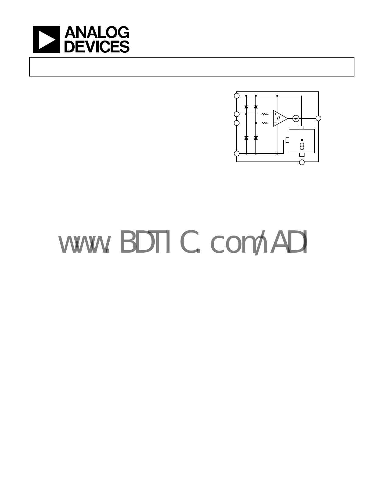
FUNCTIONAL BLOCK DIAGRAM
1
V
S
2
+IN
8
–IN
2.4V
REGULATOR
3
V
REG
6
GND
Figure 1.
AD8214
5
OUT
06193-001
GENERAL DESCRIPTION
The AD8214 is a fast, high common-mode voltage threshold
detector, which operates with a single supply of 5 V to 65 V.
Internally the AD8214 features a fast comparator that is
optimized for high side operation. It also includes a stable
2.4 V series regulator, which is referenced with respect to the
supply voltage. The purpose of the regulator is to provide
power to the internal electronics, and set an input comparison
threshold below the supply voltage. The inputs of the AD8214
may be operated at, slightly above, or below the power supply.
The differential voltage range between the inputs of the
AD8214 is 500 mV.
The device features a current output. This current is <100 nA
when –IN > +IN and 1 mA when +IN > –IN. The input
voltages are referenced to the supply voltage, as is the
internal 2.4 V regulator. The input-to-output response time
is typically <100 ns.
As the output switches from low to high, a small hysteresis
(10 mV) is activated to minimize the effects of noise in the
system, and prevent any false state conditions.
The AD8214 is available in an 8-lead MSOP package. The
operating temperature range is –40°C to +125°C, making it
ideal for industrial, consumer, and automotive applications.
Rev. 0
Information furnished by Analog Devices is believed to be accurate and reliable. However, no
responsibility is assumed by Anal og Devices for its use, nor for any infringements of patents or ot her
rights of third parties that may result from its use. Specifications subject to change without notice. No
license is granted by implication or otherwise under any patent or patent rights of Analog Devices.
Trademarks and registered trademarks are the property of their respective owners.
One Technology Way, P.O. Box 9106, Norwood, MA 02062-9106, U.S.A.
Tel: 781.329.4700 www.analog.com
Fax: 781.461.3113 ©2006 Analog Devices, Inc. All rights reserved.

AD8214
www.BDTIC.com/ADI
TABLE OF CONTENTS
Features .............................................................................................. 1
Applications....................................................................................... 1
Functional Block Diagram .............................................................. 1
General Description......................................................................... 1
Revision History ............................................................................... 2
Specifications..................................................................................... 3
Absolute Maximum Ratings............................................................ 4
ESD Caution.................................................................................. 4
Pin Configuration and Function Descriptions............................. 5
Typical Performance Characteristics ............................................. 6
REVISION HISTORY
10/06—Revision 0: Initial Version
Theory of Operation ...................................................................... 10
Comparator Offset and Hysteresis........................................... 11
Setting the Input Threshold Voltage........................................ 11
Input-Referred Dynamic Error ................................................ 11
Applications..................................................................................... 12
Typical Setup and Calculations ................................................ 12
High Side Overcurrent Detection ............................................ 13
Outline Dimensions ....................................................................... 14
Ordering Guide .......................................................................... 14
Rev. 0 | Page 2 of 16

AD8214
www.BDTIC.com/ADI
SPECIFICATIONS
VS = 13.5 V, unless otherwise noted.
Table 1.
Parameter Conditions/Comments Min Typ Max Unit
VOLTAGE OFFSET
= 25°C, voltage at –IN decreasing
Offset Voltage (RTI)
T
A
Over Temperature (RTI) ±2.5 mV
Offset Drift 15 µV/°C
HYSTERESIS
T
= 25°C, voltage at –IN increasing
A
8 10 12 mV
INPUT
Input Impedance
Differential 2 MΩ
Common Mode VS = 5 V to 65 V 5 MΩ
Voltage Range
Differential Maximum voltage between +IN and –IN 500 mV
Common Mode
V
– 0.9 VS + 0.2 V
S
Input Bias Current +IN or –IN 12 20 nA
OUTPUT
Output Current R
R
Rise Time 20% to 80%, R
20% to 80%, R
Fall Time 20% to 80%, R
20% to 80%, R
= 3.3 kΩ, output high 0.8 1 1.2 mA
OUT
= 3.3 kΩ, output low 100 nA
OUT
= 3.3 kΩ, VOD = 5 mV, 50 mV step 90 ns
OUT
= 3.3 kΩ, V
OUT
= 3.3 kΩ, VOD = 5 mV, 50 mV step 110 ns
OUT
= 3.3 kΩ, V
OUT
= >20 mV, 50 mV step 75 ns
OD
= >10 mV, 50 mV step 100 ns
OD
REGULATOR
Nominal Value
T
= 25°C, voltage from V
A
T
= –40°C to +125°C
A
REG
to V
S
2.43 V
±5 %
DYNAMIC RESPONSE 50 mV to 250 mV step
Propagation Delay
1
5 mV ≤ VOD ≤ 15 mV, output low to high 90 ns
15 mV ≤ VOD ≤ 30 mV, output low to high 80 ns
V
INPUT-REFERRED DYNAMIC ERROR
2
≥ 30 mV, output low to high 75 ns
OD
15 mV
POWER SUPPLY
Operating Range
Maximum Voltage GND to V
Minimum Voltage GND to V
Output Voltage Range
3
With respect to V
S
S
REG
65 V
5 V
2 62.5 V
Supply Current Output low 240 µA
Output high 1.2 mA
TEMPERATURE RANGE FOR SPECIFIED PERFORMANCE −40 +125 °C
1
VOD represents the overdrive voltage, or the amount of voltage by which the threshold point has been exceeded.
2
See the section. Input-Referred Dynamic Error
3
The voltage at OUT must not be allowed to exceed the V
output current is 1 mA, the load resistor must not be more than (5 V – 2.4 V)/{1 mA × (1 + 20%)}, or 2.17 kΩ, to ensure the signal does not exceed 2.6 V. As the supply
increases, the output signal also can be increased, by the same amount.
voltage, which is always 2.4 V less than the supply. For example, when the supply voltage is 5 V and the
REG
±1
±3 mV
Rev. 0 | Page 3 of 16
AD8214
www.BDTIC.com/ADI
ABSOLUTE MAXIMUM RATINGS
T
= –40°C to +125°C
A
Table 2.
Parameter Rating
Supply Voltage 65 V
Continuous Input Voltage 68 V
Reverse Supply Voltage 0.3 V
Operating Temperature Range −40°C to +125°C
Storage Temperature Range −65°C to +150°C
Output Short-Circuit Duration Indefinite
Stresses above those listed under Absolute Maximum Ratings
may cause permanent damage to the device. This is a stress
rating only; functional operation of the device at these or any
other conditions above those indicated in the operational
section of this specification is not implied. Exposure to absolute
maximum rating conditions for extended periods may affect
device reliability.
ESD CAUTION
Rev. 0 | Page 4 of 16
AD8214
www.BDTIC.com/ADI
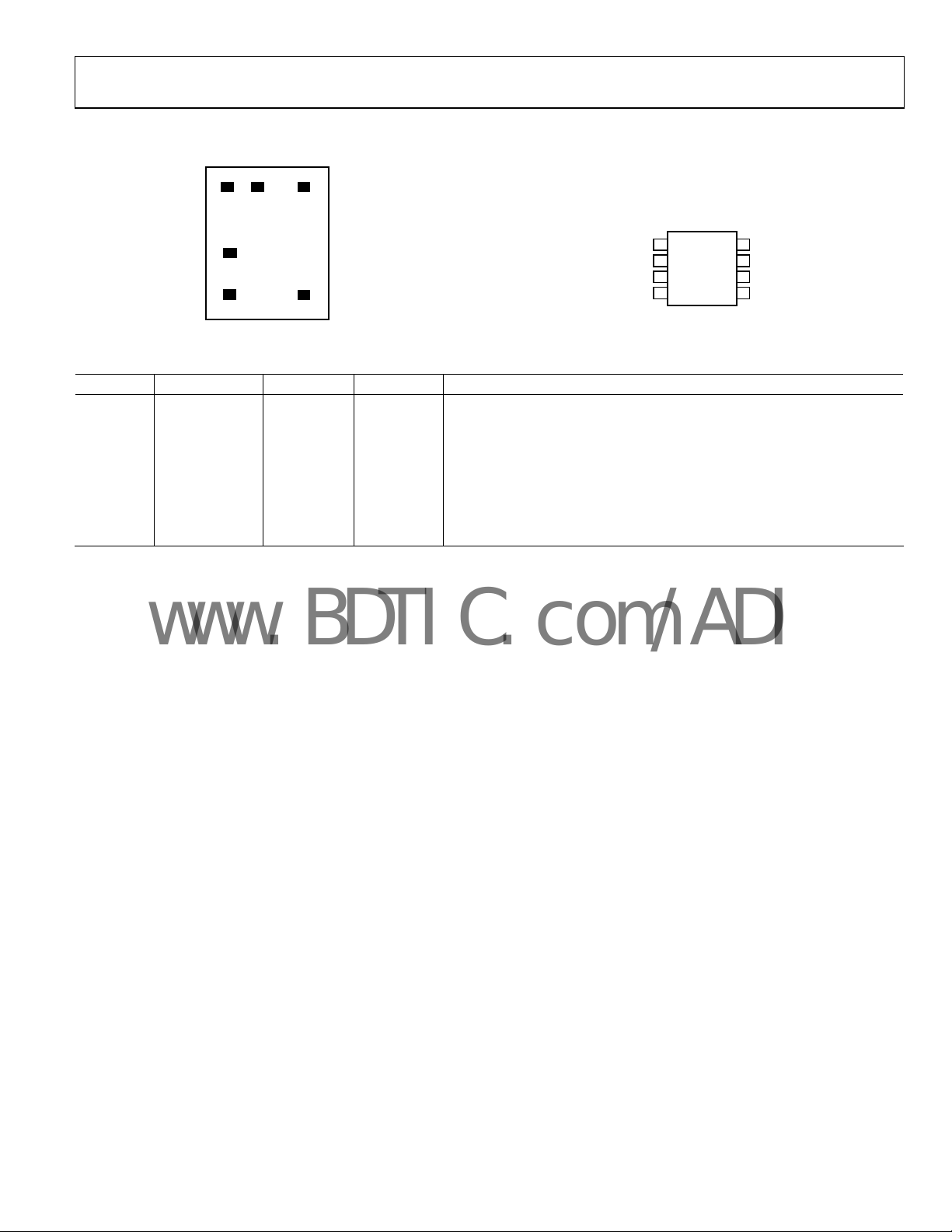
PIN CONFIGURATION AND FUNCTION DESCRIPTIONS
1 6 8
1
2
3
Figure 2. Metallization Diagram
5
06193-007
Table 3. Pin Function Descriptions
Pin No. Mnemonic X Y Description
1 V
S
–196 +447 Supply Voltage.
2 +IN –198 –58 Noninverting Input.
3 V
REG
–196 –346 Regulator Voltage.
4 NC No Connect.
5 OUT +196 –348 Output.
6 GND +196 +447 Ground.
7 NC No Connect.
8 –IN –31 +449 Inverting Input.
V
S
AD8214
+IN
2
TOP VIEW
(Not to Scale)
3
V
REG
NC
4
NC = NO CONNECT
Figure 3. Pin Configuration
–IN
8
7
NC
6
GND
5
OUT
06193-002
Rev. 0 | Page 5 of 16

AD8214
www.BDTIC.com/ADI
TYPICAL PERFORMANCE CHARACTERISTICS
16
0
15
14
13
12
INPUT BIAS CURRENT (nA)
11
10
–1.2 –1.0 –0.8 –0.6 –0.4 –0.2 0.20
INPUT COMMO N-MODE VOL TAGE (V)
5V
65V
Figure 4. Input Bias Current vs. Input Common-Mode Voltage
(With Respect to V
1.11
1.09
1.07
1.05
1.03
OUTPUT CURRENT (mA)
1.01
0.99
)
S
–0.4
–0.8
–1.2
INPUT OFFSET VOLTAGE (mV)
–1.6
06193-041
–2.0
–0.9 –0.8 –0.7 –0.6 –0. 5 –0.4 –0.3 –0.2 0.2–0.1 0 0.1
INPUT COMMON-MODE VOL TAGE (V)
06193-035
Figure 7. Input Offset Voltage vs. Input Common-Mode Voltage
(With Respect to V
280
270
260
250
240
SUPPLY CURRENT ( µA)
230
TA = –40°C
TA = +125°C
S
TA = +25°C
)
0.97
–1.40 –1.15 –0.90 –0.65 –0.40 –0.15 0.10
INPUT COMMON-MODE VOLTAGE (V)
06193-024
Figure 5. Output Current (Output High) vs. Input Common-Mode Voltage
(With Respect to V
4
2
0
–2
INPUT OFFSET VOLTAGE (mV)
–4
–40 –25 –10 5 20 35 50 65 80 95 110 125
TEMPERATURE ( °C)
)
S
06193-018
Figure 6. Input Offset Voltage vs. Temperature
220
5 152535455565
SUPPLY VOLTAGE (V)
Figure 8. Supply Current vs. Supply Voltage
(Output Low)
1.25
1.24
1.23
1.22
1.21
1.20
SUPPLY CURRENT ( mA)
1.19
1.18
5 152535455565
TA = –40°C
TA = +25°C
TA = +125°C
SUPPLY VOLTAGE (V)
Figure 9. Supply Current vs. Supply Voltage
(Output High)
06193-023
06193-034
Rev. 0 | Page 6 of 16

AD8214
www.BDTIC.com/ADI
2.448
2.444
2.440
2.436
REGULATOR VOLTAGE (V)
2.432
2.428
5 15253545556
TA = +125°C
TA = +25°C
TA = –40°C
SUPPLY VOLTAGE (V)
Figure 10. Regulator Voltage vs. Supply Voltage
and VS)
REG
TA = +25°C
2.50
2.45
2.40
(Between V
TA = +125°C
TA = –40°C
06193-022
5
1.10
= +125°C
T
1.05
1.00
OUTPUT CURRENT (mA)
0.95
0.90
A
= +25°C
T
A
TA = –40°C
5 152535455565
SUPPLY VOLTAGE (V)
Figure 13. Output Current vs. Supply Voltage
(Output High)
12.0
11.5
11.0
10.5
10.0
06193-020
2.35
REGULATOR VOLTAG E (V)
2.30
10 50 100 150 200
REGULATOR LOAD RESISTANCE (k)
Figure 11. Regulator Voltage vs. Regulator Load Resistance
(Series Resistance Between V
700
600
500
400
300
200
OUTPUT CURRENT (nA)
= +25°C
T
A
100
0
5 152535455565
SUPPLY VOLTAGE (V)
and VS)
REG
TA = +125°C
TA = –40°C
Figure 12. Output Current vs. Supply Voltage
(Output Low)
9.5
9.0
HYSTERESIS VOL TAGE (mV)
8.5
06193-021
8.0
–40 –25 –10 5 20 35 50 65 80 95 110 125
TEMPERATURE (° C)
06193-017
Figure 14. Hysteresis Voltage vs. Temperature
(–IN Increasing)
170
150
130
110
FALL TIME (ns)
90
70
06193-019
50
15 25 35 45 55 65 75 85 95
R
= 5k
OUT
R
= 3.3k
OUT
OVERDRIVE VOLTAGE (mV)
06193-027
Figure 15. Fall Time vs. Overdrive Voltage
(–IN > +IN by Specified V
)
OD
Rev. 0 | Page 7 of 16

AD8214
www.BDTIC.com/ADI
110
–IN
30mV/DIV
R
= 5k
R
OUT
OUT
= 3.3k
OUT
2V/DIV
90
RISE TIM E (ns)
70
VOD = 50mV
VOD = 30mV
+IN
50
5 152535455565758595
OVERDRIVE VOLTAGE (mV)
Figure 16. Rise Time vs. Overdrive Voltage
(+IN > –IN by Specified V
–IN
10mV/DIV
VOD = 15mV
VOD = 5mV
OUT
2V/DIV
100ns/DIV
Figure 17. Typical Propagation Delay (R
–IN
10mV/DIV
VOD = 20mV
)
OD
+IN
= 5 kΩ)
OUT
+IN
06193-028
Figure 19. Typical Propagation Delay (R
–IN 50mV/DIV
OUT
2V/DIV
06193-029
Figure 20. Typical Propagation Delay (R
190
170
150
100ns/DIV
VOD = 100mV
VOD = 100mV
100ns/DIV
= 5 kΩ)
OUT
+IN
= 5 kΩ)
OUT
06193-031
06193-032
130
VOD = 10mV
OUT
2V/DIV
100ns/DIV
Figure 18. Typical Propagation Delay (R
OUT
06193-030
= 5 kΩ)
110
90
PROPAGATI ON DELAY (ns)
70
50
15 25 35 45 55 65 75 85 95
OVERDRIVE VO LTAGE (mV)
Figure 21. Propagation Delay vs. Overdrive Voltage
(–IN > +IN by Specified V
Rev. 0 | Page 8 of 16
R
= 5k
OUT
R
= 3.3k
OUT
, Output High to Low)
OD
06193-026

AD8214
www.BDTIC.com/ADI
120
110
100
90
80
PROPAGATI ON DELAY (n s)
70
60
5 152535455565758595
R
= 3.3k
OUT
R
= 5k
OUT
OVERDRIVE VO LTAGE (mV)
Figure 22. Propagation Delay vs. Overdrive Voltage,
(+IN > –IN by Specified V
, Output Low to High)
OD
06193-025
240
210
180
150
120
COUNT
90
60
30
0
–12.0 –11.5 –11.0 –10. 5 –10.0 –9.5 –9.0 –8.5 –8.0
HYSTERESIS VOLTAGE (mV)
MEAN = –10
Figure 25. Hysteresis Voltage Distribution
06193-040
12
11
10
9
HYSTERESIS VOLTAGE (mV)
8
7
–0.9–1.0 –0.8 –0.7 –0.6 –0.5 –0.4 –0.3 –0.2 0.2–0.1 0 0.1
INPUT COMMO N-MODE VOL TAGE (V)
Figure 23. Hysteresis Voltage vs. Input Common-Mode Voltage
(With Respect to V
140
120
100
80
COUNT
60
40
20
0
–4 –2–3 –1 401 32
INPUT OFFSET VOLTAGE ( mV)
)
S
Figure 24. Input Offset Voltage Distribution
MEAN = –0.16
240
210
180
150
120
COUNT
90
60
30
06193-037
0
800 850 900 950 1000 1050 1100 1150 1200
OUTPUT CURRENT (µA)
MEAN = 987.7
06193-039
Figure 26. Output Current Distribution
160
140
120
100
80
COUNT
60
40
20
06193-036
0
–2.46 –2. 45 –2.44 –2.43 –2.42 –2.40–2.41
REGULATOR VOLTAGE (V)
MEAN = –2.42
06193-038
Figure 27. Regulator Voltage Distribution
(With Respect to V
)
S
Rev. 0 | Page 9 of 16

AD8214
T
V
www.BDTIC.com/ADI
THEORY OF OPERATION
The AD8214 is a high voltage comparator offering an input-tooutput response time of less than 100 ns. This device is ideal for
detecting overcurrent conditions on the high side of the control
loop. The AD8214 is designed specifically to facilitate and allow
for fast shutdown of the control loop, preventing damage due to
excessive currents to the FET, load, or shunt resistor.
The AD8214 operates with a supply of 5 V to 65 V. It combines
a fast comparator, optimized for high side operation, with a
2.4 V series voltage regulator. The regulator provides a stable
voltage that is negative with respect to the positive supply rail,
and it is intended to provide power to the internal electronics,
set a comparison threshold below the supply rail, and power
small application circuits used with the comparator.
The differential input of the comparator may be operated at, or
slightly above or below, the positive supply rail. Typically, one of
the comparator inputs is driven negative with respect to the
positive supply by a small series resistor carrying the main
supply current to the load. The other input of the comparator
connects to a voltage divider across the regulator, so the
comparator trips as the voltage across the series resistor crosses
the user-selected threshold.
The AD8214 features a current output. The current is low (100 nA
typical), until the user selected threshold is crossed. After this point
the output switches to high (1 mA typical). The current output
driver complies with load voltage from 0 V to (V
– 2.4 V). The
S
current easily drives a ground referenced resistor to develop logic
levels determined by the value of the load resistor.
The comparator input is balanced to switch as the inverting
input (–IN) is driven negative with respect to the noninverting
input (+IN). As the comparator output switches from 0 mA to
1 mA, a small hysteresis (10 mV) is activated to minimize the
effects of noise in the system that may be triggered by the
comparator signal. This means that to restore the output to zero,
the input polarity must be reversed by 10 mV beyond the
original threshold.
BATTERY
SHUNT
VOLTAGE DROP
ACROSS SHUNT
CORRESPONDING
O CURRENT LEVEL
TO LOAD
I
CONSTANT
THRESHOLD
R1
+
_
R2
1
+
_
2
8
3
Figure 28. Simplified Schematic
2.4V
REGULAT OR
6
5
CONSTAN T
2.4V
UP TO 65
2
1
3
06193-005
Rev. 0 | Page 10 of 16

AD8214
www.BDTIC.com/ADI
COMPARATOR OFFSET AND HYSTERESIS
The AD8214 features built-in hysteresis to minimize the effects
of noise in the system. There is also a small offset at the input of
the device.
V
OH
values for these resistors can be chosen based on the desired
threshold voltage using the equation:
4.2
⎛
⎜
⎝
⎞
⎟
+
R2R1
⎠
)(
INTHVR1
+=×
(1)
For proper operation it is recommended that the internal 2.4 V
regulator not be loaded down by using small R1 and R2 values.
Figure 11 shows the proper range for the total series resistance.
V
H
V
OL
VOS = INPUT OFFSET VOLTAGE
V
= HYSTERESIS VOLTAGE
H
V
= THRESHOLD VOLTAGE
TH
V
= OUTPUT HI GH
OH
V
= OUTPUT LOW
OL
Figure 29. Hysteresis and Input Offset Voltage Definition
V
OS
V
TH
06193-033
Figure 29 shows the relationship between the input voltage and the
output current. The horizontal axis represents the voltage between
the positive (+IN) and negative (–IN) inputs of the AD8214. The
vertical axis shows the output current for a given input voltage.
V
represents the point where the inputs are at the same voltage
TH
level (+IN = –IN). The output of the AD8214 remains low (V
)
OL
provided (–IN) is at a higher voltage potential than (+IN). As the
input voltage transitions to +IN > –IN, the output switches states.
Under ideal conditions, the output is expected to change states at
exactly V
equal ± a small offset voltage (V
. In practice, the output switches when the inputs are
TH
).
OS
Once the output switches from low to high, it remains in this state
until the input voltage falls below the hysteresis voltage. Typically,
this occurs when +IN is 10 mV below –IN.
SETTING THE INPUT THRESHOLD VOLTAGE
The AD8214 features a 2.4 V series regulator, which can be used
to set a reference threshold voltage with two external resistors.
The resistors constitute a voltage divider, the middle point of
which connects to +IN. The total voltage across the resistors is
always 2.4 V. (See Figure 28 for proper resistor placement.) The
INPUT-REFERRED DYNAMIC ERROR
Frequently, the dynamics of comparators are specified in terms
of propagation delay of the response at the output to an input
pulse crossing the threshold between two overload states. For
this measurement, the rise time of the input pulse is negligible
compared to the comparator propagation delay. In the case of
the AD8214, this propagation delay is typically 100 ns, when the
input signal is a fast step.
The primary purpose of the AD8214 is to monitor for overcurrent conditions in a system. It is much more common that in
such systems, the current in the path increases slowly; therefore,
the transition between two input overload conditions around
the threshold is slow relative to the propagation delay. In some
cases, this transition can be so slow that the time from the
actual threshold crossing to the output signal switching states is
longer than the specified propagation delay, due to the
comparator dynamics.
If the voltage at the input of the AD8214 is crossing the set
threshold at a rate ≤100 mV/µs, the output switches states
before the threshold voltage has been exceeded by 15 mV.
Therefore, if the input signal is changing so slowly that the
propagation delay is affected, the error that accumulates at the
input while waiting for the output response is proportionately
smaller and, typically, less than 15 mV for ramp rates
≤100 mV/µs.
Rev. 0 | Page 11 of 16

AD8214
k
www.BDTIC.com/ADI
APPLICATIONS
TYPICAL SETUP AND CALCULATIONS
The key feature of the AD8214 is its ability to detect an overcurrent
condition on the high side of the rail and provide a signal in less
than 100 ns. This performance protects expensive loads, FETs, and
shunt resistors in a variety of systems and applications. This section
details a typical application in which the normal current in the
system is less ≤10 A and an overcurrent detection is necessary
when 15 A is detected in the path.
If we assume a shunt resistance (R
common-mode voltage range of 5 V to 65 V, the typical voltage
across the shunt resistor is
10 A × 0.005 Ω = 50 mV
The voltage drop across the shunt resistor, in the case of an
overcurrent condition is
15 A × 0.005 Ω = 75 mV
The threshold voltage, must therefore be set at 75 mV,
corresponding to the overcurrent condition. R1 and R2 can be
selected based on this 75 mV threshold at the positive input of
the comparator.
A low load current across the regulator corresponds to optimal
regulator performance; therefore, the series resistance of R1 and
R2 must be relatively large. For this case, the total resistance can
be set as
R1 + R2 = 200 kΩ
To have a 75 mV drop across R1, the following calculations apply:
2.4V
200
mV 75
µA 12
Ω
µA 12
=
R1 k 6.25
=Ω=
R2 = (200 kΩ – R1) = 193.75 kΩ
The values for R1 and R2 are set; correspondingly, the threshold
voltage at +IN is set at 75 mV.
) of 0.005 Ω and a
SHUNT
BATTERY
Under normal operating conditions, the current is 10 A or less,
corresponding to a maximum voltage drop across the shunt of
50 mV. This means that the negative input of the comparator is
50 mV below the battery voltage. Since the positive input is
75 mV below the battery voltage, the negative input is at a
higher potential than the positive; therefore, the output of the
AD8214 is low.
If the current increases to 15 A, the drop across the shunt is
75 mV. As the current continues to increase, the positive input
of the comparator reaches a higher potential than the negative,
and the output of the AD8214 switches from low to high. The
input-to-output response of the AD8214 is less than 100 ns. The
output resistor in this case is selected so that the logic level high
signal is 3.3 V.
The output changes states from low to high in the case of an
overcurrent condition. However, the input offset voltage is
typically 1 mV; therefore, this must be taken into consideration
when choosing the threshold voltage. When the current in the
system drops back down to normal levels, the AD8214 changes
states from high to low. However, due to the built-in 10 mV
hysteresis, the voltage at (–IN) must be 10 mV higher than the
threshold for the output to change states from high to low. This
built-in hysteresis is intended to prevent input chatter as well as
any false states.
Table 4 shows typical resistors combinations that can be used to set
an input threshold voltage. Numbers are based on a 2.43 V V
REG
.
Table 4.
Threshold (mV) R1 (kΩ) R2 (kΩ)
30 1.5 120
50 1.6 75
60 2 80
75 2.4 75
110 8.06 169
1
R1
6.25k
2
8
3
Figure 30. Typical Application
2.4V
REGULATOR
6
I
OUT
5
R
OUT
R
SHUNT
(0.005)
I
I
LOAD
C1
0.01µF
193.75k
R2
Rev. 0 | Page 12 of 16
V
OUT
= 3.3k
06193-006

AD8214
www.BDTIC.com/ADI
HIGH SIDE OVERCURRENT DETECTION
The AD8214 is useful for many automotive applications using the
load configuration shown in Figure 31. Because the part powers
directly from the battery voltage, the shunt resistor must be on
the high side. The AD8214 monitors the current in the path as
long as the battery voltage is between 5 V and 65 V. If the current
reaches an undesirable level that corresponds to the user-selected
threshold, the output of the AD8214 switches states in less than
100 ns. The microcontroller, analog-to-digital converter, or FET
driver can be directly notified of this condition.
I
SHUNT
CLAMP
DIODE
7
6
5
SWITCH
OVERCURRENT
DETECTIO N (<100ns)
AD8214
1 8
V
R1
C1
R2
S
+IN
2
3
V
REG
4
NC
Figure 31. High Side Overcurrent Protection
–IN
NC
GND
OUT
BATTERY
UP TO 65V
06193-004
Rev. 0 | Page 13 of 16

AD8214
www.BDTIC.com/ADI
OUTLINE DIMENSIONS
3.20
3.00
2.80
8
5
3.20
3.00
1
2.80
PIN 1
0.65 BSC
0.95
0.85
0.75
0.15
0.38
0.00
0.22
COPLANARITY
0.10
COMPLIANT TO JEDEC STANDARDS MO-187-AA
Figure 32. 8-Lead Mini Small Outline Package [MSOP]
ORDERING GUIDE
Model Temperature Range Package Description Package Option Branding
AD8214ARMZ
AD8214ARMZ-RL1 −40°C to +125°C 8-Lead MSOP, 13” Tape and Reel RM-8 H0N
AD8214ARMZ-R71 −40°C to +125°C 8-Lead MSOP, 7” Tape and Reel RM-8 H0N
1
Z = Pb-free part.
1
−40°C to +125°C 8-Lead MSOP RM-8 H0N
5.15
4.90
4.65
4
1.10 MAX
8°
0°
SEATING
PLANE
0.23
0.08
(RM-8)
Dimensions shown in millimeters
0.80
0.60
0.40
Rev. 0 | Page 14 of 16

AD8214
www.BDTIC.com/ADI
NOTES
Rev. 0 | Page 15 of 16

AD8214
www.BDTIC.com/ADI
NOTES
©2006 Analog Devices, Inc. All rights reserved. Trademarks and
registered trademarks are the property of their respective owners.
D06193-0-10/06(0)
Rev. 0 | Page 16 of 16
 Loading...