V
High-Side, Bidirectional
Preliminary Technical Data
FEATURES
Precision bidirectional current sensing
High common-mode voltage range
−2 V to +65 V operating
Gain = 20
CMRR = 100 dB
Wide operating temperature range
Die: −40°C to +150°C
8-lead SOIC: −40°C to +125°C
Adjustable offset
Available in SOIC and die form
EXCELLENT AC AND DC PERFORMANCE
5 µV/°C offset drift
30 ppm/°C gain drift
80 dB CMRR dc to 10 kHz
APPLICATIONS
42 V dc-to-dc converter current sensing
High-side current sensing
Motor controls
Transmission controls
Diesel injection controls
Engine management
Suspension controls
Vehicle dynamic controls
SUPPLY
Current Shunt Monitor
AD8210
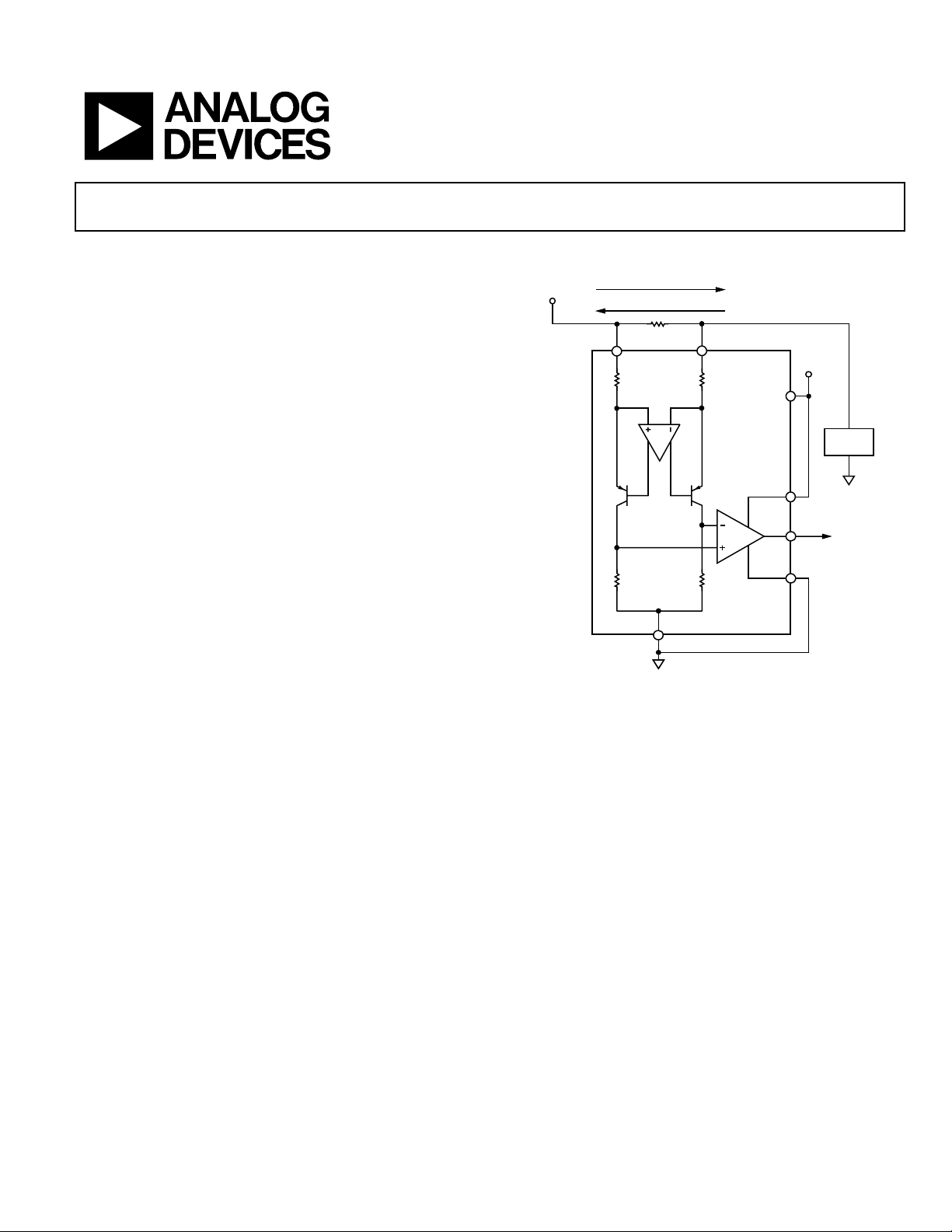
TYPICAL OPERATING CIRCUIT
I
S
R
S
+IN –IN
GND
AD8210
G = +20
Figure 1.
V
REF
V
REF
V+
V
S
1
2
LOAD
VOUT
05147-001
GENERAL DESCRIPTION
The AD8210 is a high-side, single-supply, bidirectional current
shunt monitor that features a wide input, common-mode voltage range of −2 V to +65 V, high bandwidth, a set gain of 20, and
a typical 5 V supply voltage.
The AD8210 is offered in die and packaged form. The operating
temperature range for the die is 25°C higher (up to 150°C) than
that of the packaged part, which enables the user to apply the
AD8210 in high temperature applications.
Rev. PrB
Information furnished by Analog Devices is believed to be accurate and reliable.
However, no responsibility is assumed by Analog Devices for its use, nor for any
infringements of patents or other rights of third parties that may result from its use.
Specifications subject to change without notice. No license is granted by implication
or otherwise under any patent or patent rights of Analog Devices. Trademarks and
registered trademarks are the property of their respective owners.
Excellent ac and dc performance over temperature keeps errors
in the measurement loop to a minimum. Offset drift is typically
below 5 µV/°C, and the gain drift is typically below 30 ppm/°C.
Bidirectional current measurement is achieved by offsetting the
output between 0.05 V and 4.8 V with a 5 V supply. With the
2 pin connected to the V+ pin, and the V
V
REF
1 pin connected
REF
to the GND pin, the output is set at half scale. Attaching both
pins to GND causes the output to be unipolar, starting near
V
REF
ground. Attaching both V
pins to V+ causes the output to be
REF
unipolar starting near V+. Other offsets can be obtained by
applying an external voltage to V
One Technology Way, P.O. Box 9106, Norwood, MA 02062-9106, U.S.A.
Tel: 781.329.4700
Fax: 781.326.8703 © 2005 Analog Devices, Inc. All rights reserved.
www.analog.com
1 and V
REF
2 pins.
REF

AD8210 Preliminary Technical Data
TABLE OF CONTENTS
Specifications..................................................................................... 3
Bidirectional Operation................................................................9
Absolute Maximum Ratings............................................................ 4
ESD Caution.................................................................................. 4
Pin Configuration and Function Descriptions............................. 5
Typical Performance Characteristics............................................. 6
Theory of Operation ........................................................................ 8
Output Offset Adjustment............................................................... 9
Unidirectional Operation............................................................ 9
Ground Referenced Output ........................................................ 9
V+ Referenced Output................................................................. 9
REVISION HISTORY
1/05—Revision PrB: Preliminary Version
External Reference Output........................................................ 10
Splitting an External Reference ................................................ 10
Splitting the Supply .................................................................... 10
Applications..................................................................................... 11
High-Side Current Sense with a Low-Side Switch................. 11
High-Side Current Sense with a High-Side Switch ............... 11
Outline Dimensions....................................................................... 12
Ordering Guide .......................................................................... 12
Rev. PrB | Page 2 of 12

Preliminary Technical Data AD8210
SPECIFICATIONS
TA = operating temperature range, VS = 5 V, unless otherwise noted.
Table 1.
AD8210 SOIC AD8210 Die
Parameter Conditions Min Typ Max Min Typ Max Unit
GAIN
Gain 20 20 V/V
Accuracy VO ≥ 0.1 V dc ±0.5 ±1 ±0.5 ±1.5 %
Accuracy Over Temperature Specified temperature range ±1.5 ±2.5 %
Gain vs. Temperature ±20 ±30 ppm/°C
VOLTAGE OFFSET
Offset Voltage (RTI) 25°C ±1 ±2 mV
Over Temperature (RTI) Specified temperature range ±2 ±4 mV
Offset Drift 5 10 µV/°C
INPUT
Input Impedance
Differential 2 2 kΩ
Common Mode V common-mode > 5 V 5 5 MΩ
Common Mode V common-mode < 5 V 3.5 3.5 kΩ
Input Voltage Range Common-mode, continuous −2 +65 −2 +65 V
Input Voltage Range Differential, unconditional 250 250 mV
Input Voltage Range Differential ±125 ±125 mV
Common-Mode Rejection f = 1 kHz 100 dB
Common-Mode Rejection f = 10 kHz 100 90 dB
OUTPUT
Output Voltage Range 0.05 4.8 0.05 4.8 V
DYNAMIC RESPONSE
Small Signal −3 dB Bandwidth 500 500 kHz
Slew Rate 3 3 V/µs
NOISE
0.1 Hz to 10 Hz, RTI TBD TBD µV p-p
Spectral Density, 1 kHz, RTI TBD TBD µV/√Hz
OFFSET ADJUSTMENT
Offset Adjustment Range VS = 5 V 0.05 4.8 0.05 4.8 V
POWER SUPPLY
Operating Range For specified performance 4.5 5.5 4.5 5.5 V
Quiescent Current Over Temperature VO = 0.1 V dc 0.5 1 0.5 1 mA
Power-Supply Rejection Ratio 80 80 dB
TEMPERATURE RANGE
For Specified Performance Operating temperature range −40 +125 −40 +150 °C
Rev. PrB | Page 3 of 12

AD8210 Preliminary Technical Data
ABSOLUTE MAXIMUM RATINGS
Table 2.
Parameter Rating
Supply Voltage 12 V
Continuous Input Voltage 65 V
Transient Input Voltage 72 V
Reverse Supply Voltage −0.3 V
Negative Common-Mode Range −2.3 V
Operating Temperature Range −40°C to +125°C
Storage Temperature −65°C to +150°C
Lead Temperature Range 300°C
ESD CAUTION
ESD (electrostatic discharge) sensitive device. Electrostatic charges as high as 4000 V readily accumulate on
the human body and test equipment and can discharge without detection. Although this product features proprietary ESD protection circuitry, permanent damage may occur on devices subjected to high energy electrostatic discharges. Therefore, proper ESD precautions are recommended to avoid performance degradation or
loss of functionality.
Stresses above those listed under Absolute Maximum Ratings
may cause permanent damage to the device. This is a stress
rating only; functional operation of the device at these or any
other conditions above those indicated in the operational section of this specification is not implied. Exposure to absolute
maximum rating conditions for extended periods may affect
device reliability.
Rev. PrB | Page 4 of 12
 Loading...