

High Voltage, Bidirectional
V
www.BDTIC.com/ADI
FEATURES
±4000 V HBM ESD
High common-mode voltage range
−2 V to +65 V operating
−5 V to +68 V survival
Buffered output voltage
5 mA output drive capability
Wide operating temperature range: −40°C to +125°C
Ratiometric half-scale output offset
Excellent ac and dc performance
1 μV/°C typical offset drift
10 ppm/°C typical gain drift
120 dB typical CMRR at dc
80 dB typical CMRR at 100 kHz
Available in 8-lead SOIC
APPLICATIONS
Current sensing
Motor controls
Transmission controls
Diesel injection controls
Engine management
Suspension controls
Vehicle dynamic controls
DC-to-dc converters
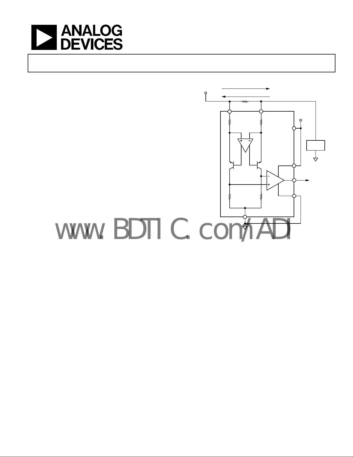
Current Shunt Monitor
AD8210
FUNCTIONAL BLOCK DIAGRAM
SUPPLY
I
S
R
S
+IN –IN
GND
Figure 1.
AD8210
V
REF
G=+20
V
REF
V+
V
S
LOAD
1
VOUT
2
05147-001
GENERAL DESCRIPTION
The AD8210 is a single-supply, difference amplifier ideal for
amplifying small differential voltages in the presence of large
common-mode voltages. The operating input common-mode
voltage range extends from −2 V to +65 V. The typical supply
voltage is 5 V.
The AD8210 is offered in a SOIC package. The operating
emperature range is −40°C to +125°C.
t
Excellent ac and dc performance over temperature keep errors
in t
he measurement loop to a minimum. Offset drift and gain
drift are guaranteed to a maximum of 8 µV/°C and 20 ppm/°C,
respectively.
Rev. A
Information furnished by Analog Devices is believed to be accurate and reliable. However, no
responsibility is assumed by Anal og Devices for its use, nor for any infringements of patents or ot her
rights of third parties that may result from its use. Specifications subject to change without notice. No
license is granted by implication or otherwise under any patent or patent rights of Analog Devices.
Trademarks and registered trademarks are the property of their respective owners.
The output offset can be adjusted from 0.05 V to 4.9 V with
a 5
V supply by using the V
V
1 pin attached to the V+ pin and the V
REF
1 pin and the V
REF
2 pin. With the
REF
2 pin attached to
REF
the GND pin, the output is set at half scale. Attaching both V
and V
near ground. Attaching both V
2 to GND causes the output to be unipolar, starting
REF
1 and V
REF
2 to V+ causes the
REF
output to be unipolar, starting near V+. Other offsets can be
obtained by applying an external voltage to V
1 and V
REF
One Technology Way, P.O. Box 9106, Norwood, MA 02062-9106, U.S.A.
Tel: 781.329.4700 www.analog.com
Fax: 781.461.3113 ©2006–2007 Analog Devices, Inc. All rights reserved.
REF
REF
1
2.

AD8210
www.BDTIC.com/ADI
TABLE OF CONTENTS
Features .............................................................................................. 1
Applications....................................................................................... 1
Functional Block Diagram .............................................................. 1
General Description......................................................................... 1
Revision History ............................................................................... 2
Specifications..................................................................................... 3
Absolute Maximum Ratings............................................................ 4
ESD Caution.................................................................................. 4
Pin Configuration and Function Descriptions............................. 5
Typical Performance Characteristics ............................................. 6
Theory of Operation ...................................................................... 10
REVISION HISTORY
4/07—Rev. 0 to Rev. A
Changes to Features.......................................................................... 1
Changes to Input Section................................................................. 3
Updated Outline Dimensions....................................................... 15
4/06—Revision 0: Initial Version
Modes of Operation ....................................................................... 11
Unidirectional Operation.......................................................... 11
Bidirectional Operation............................................................. 11
Input Filtering ................................................................................. 13
Applications Information.............................................................. 14
High-Side Current Sense with a Low-Side Switch................. 14
High-Side Current Sense with a High-Side Switch ............... 14
H-Bridge Motor Control ........................................................... 14
Outline Dimensions ....................................................................... 15
Ordering Guide .......................................................................... 15
Rev. A | Page 2 of 16

AD8210
www.BDTIC.com/ADI
SPECIFICATIONS
TA = operating temperature range, VS = 5 V, unless otherwise noted.
Table 1.
AD8210 SOIC
1
Parameter Min Typ Max Unit Conditions
GAIN
Initial 20 V/V
Accuracy ±0.5 % 25°C, VO ≥ 0.1 V dc
Accuracy Over Temperature ±0.7 % T
A
Gain Drift 20 ppm/°C
VOLTAGE OFFSET
Offset Voltage (RTI) ±1.0 mV 25°C
Over Temperature (RTI) ±1.8 mV T
A
Offset Drift ±8.0 μV/°C
INPUT
Input Impedance
Differential 2 kΩ
Common Mode 5 MΩ V common mode > 5 V
1.5 kΩ V common mode < 5 V
Common-Mode Input Voltage Range −2 +65 V Common mode, continuous
Differential Input Voltage Range 250 mV Differential
2
Common-Mode Rejection 100 120 dB TA, f = dc, VCM > 5 V
80 95 dB TA, f = dc to 100 kHz3, VCM < 5 V
80 dB TA, f = 100 kHz3, VCM > 5 V
80 dB TA, f = 40 kHz3, VCM > 5 V
OUTPUT
Output Voltage Range 0.05 4.9 V RL = 25 kΩ
Output Impedance 2 Ω
DYNAMIC RESPONSE
Small Signal −3 dB Bandwidth 450 kHz
Slew Rate 3 V/μs
NOISE
0.1 Hz to 10 Hz, RTI 7 μV p-p
Spectral Density, 1 kHz, RTI 70 nV/√Hz
OFFSET ADJUSTMENT
Ratiometric Accuracy
Accuracy, RTO ±0.6 mV/V Voltage applied to V
4
0.499 0.501 V/V Divider to supplies
REF
1 and V
2 in parallel
REF
Output Offset Adjustment Range 0.05 4.9 V VS = 5 V
V
Input Voltage Range 0.0 V
REF
V
Divider Resistor Values 24 32 40 kΩ
REF
POWER SUPPLY, V
S
S
V
Operating Range 4.5 5.0 5.5 V
Quiescent Current Over Temperature 2 mA VCM > 5 V
5
Power Supply Rejection Ratio 80 dB
TEMPERATURE RANGE
For Specified Performance −40 +125 °C
1
T
to T
MIN
2
Differential input voltage range = ±125 mV with half-scale output offset.
3
Source imbalance < 2 Ω.
4
The offset adjustment is ratiometric to the power supply when V
5
When the input common mode is less than 5 V, the supply current increases. This can be calculated with the following formula: IS = −0.7 (VCM) + 4.2 (see Fi ). gure 21
= −40°C to +125°C.
MAX
1 and V
REF
2 are used as a divider between the supplies.
REF
Rev. A | Page 3 of 16

AD8210
www.BDTIC.com/ADI
ABSOLUTE MAXIMUM RATINGS
Table 2.
Parameter Rating
Supply Voltage 12.5 V
Continuous Input Voltage (VCM) −5 V to +68 V
Reverse Supply Voltage 0.3 V
ESD Rating
HBM (Human Body Model) ±4000 V
CDM (Charged Device Model) ±1000 V
Operating Temperature Range −40°C to +125°C
Storage Temperature Range −65°C to +150°C
Output Short-Circuit Duration Indefinite
S
tresses above those listed under Absolute Maximum Ratings
may cause permanent damage to the device. This is a stress
rating only; functional operation of the device at these or any
other conditions above those indicated in the operational
section of this specification is not implied. Exposure to absolute
maximum rating conditions for extended periods may affect
device reliability.
ESD CAUTION
Rev. A | Page 4 of 16
AD8210
www.BDTIC.com/ADI
PIN CONFIGURATION AND FUNCTION DESCRIPTIONS
–IN
1
2
GND
V
2
3
REF
NC
4
NC = NO CONNECT
AD8210
TOP VIEW
(Not to Scale)
+IN
8
7
V
1
REF
V+
6
OUT
5
05147-003
Figure 2. Pin Configuration
Table 3. Pin Function Descriptions
Pin No. Mnemonic X Y
1 −IN −443 +584
2 GND −479 +428
3 V
2 −466 −469
REF
4 NC
5 OUT +466 −537
6 V+ +501 −95
7 V
1 +475 +477
REF
8 +IN +443 +584
1
2
3
Figure 3. Metallization Diagram
8
7
6
5
5147-002
Rev. A | Page 5 of 16

AD8210
www.BDTIC.com/ADI
TYPICAL PERFORMANCE CHARACTERISTICS
200
180
160
140
120
100
80
60
40
20
(µV)
0
OSI
–20
V
–40
–60
–80
–100
–120
–140
–160
–180
–200
–40
–20
–30
–100102030405060708090
TEMPERATURE (°C)
Figure 4. Typical Offset Drift
140
130
120
110
+125°C
100
CMRR (dB)
90
80
70
60
100 100k
–40°C
1k 10k
FREQUENCY ( Hz)
Figure 5. CMRR vs. Freq uency and Temperature
(
Common-Mode Voltage < 5 V)
140
130
120
110
–40°C
+125°C
100
CMRR (dB)
90
+25°C
+25°C
100
110
120
05147-030
05147-032
2000
1600
1200
800
400
0
–400
GAIN ERROR (ppm)
–800
–1200
–1600
–2000
–40
–20
–30
–100102030405060708090
TEMPERATURE ( °C)
Figure 7. Typical Gain Drift
30
25
20
15
10
5
0
–5
–10
–15
GAIN (dB)
–20
–25
–30
–35
–40
–45
–50
10 10M
100 1k 10k 100k 1M
FREQUENCY (Hz)
Figure 8. Typical Small Signal Bandwidth (V
= 200 mV p-p)
OUT
100mV/DIV
500mV/DIV
100
110
120
05147-033
5147-014
80
70
60
100 100k
Figure 6. CMRR vs. Freq uency and Temperature
1k 10k
FREQUENCY ( Hz)
(
Common-Mode Voltage > 5 V)
05147-031
Figure 9. Fall Time
Rev. A | Page 6 of 16
400ns/DIV
05147-017

AD8210
www.BDTIC.com/ADI
4V/DIV
100mV/DIV
0.02%/DIV
500mV/DIV
400ns/DIV
Figure 10. Rise Time
200mV/DIV
2V/DIV
1µs/DIV
Figure 11. Differential Overload Recovery (Falling)
200mV/DIV
05147-018
4µs/DIV
05147-024
Figure 13. Settling Time (Falling)
4V/DIV
0.02%/DIV
05147-016
4µs/DIV
05147-025
Figure 14. Settling Time (Rising)
50V/DIV
2V/DIV
1µs/DIV
Figure 12. Differential Overload Recovery (Rising)
05147-015
100mV/DIV
Figure 15. Common-Mode Response (Falling)
Rev. A | Page 7 of 16
1µs/DIV
05147-019

AD8210
www.BDTIC.com/ADI
50V/DIV
100mV/DIV
8
1µs/DIV
Figure 16. Common-Mode Response (Rising)
5.0
4.9
4.8
4.7
4.6
4.5
4.4
4.3
4.2
4.1
4.0
3.9
OUTPUT VO LTAGE RANG E (V)
3.8
3.7
3.6
3.5
06
05147-020
0.5 1.0 1.5 2.0 2.5 3.0 3.5 4.0 4.5 5.0 5.5 6.0
OUTPUT SOURCE CURRENT (mA)
.5
5147-023
Figure 19. Output Voltage Range vs. Output Source Current
1.4
7
6
5
4
3
2
1
MAXIMUM OUT PUT SINK CURRENT ( mA)
0
–40
–20 0 20 40 60 80 100 120 140
TEMPERATURE (°C)
Figure 17. Output Sink Current vs. Temperature
11
10
9
8
7
6
5
4
3
2
1
MAXIMUM OUTPUT SOURCE CURRENT (mA)
0
–40
–20 0 20 40 60 80 100 120 140
TEMPERATURE (°C)
Figure 18. Output Source Current vs. Temperature
1.2
1.0
0.8
0.6
0.4
0.2
OUTPUT VOLTAGE RANGE FROM GND (V)
0
0
1 2 3 4 5 6 7 8 9
5147-022
OUTPUT SINK CURRENT (mA)
05147-038
Figure 20. Output Voltage Range from GND vs. Output Sink Current
6.0
5.5
5.0
4.5
4.0
3.5
3.0
2.5
SUPPLY CURRENT (mA)
2.0
1.5
1.0
–2 65
5147-026
02468
COMMON-MO DE VOLTAGE (V )
05147-027
Figure 21. Supply Current vs. Common-Mode Voltage
Rev. A | Page 8 of 16
AD8210
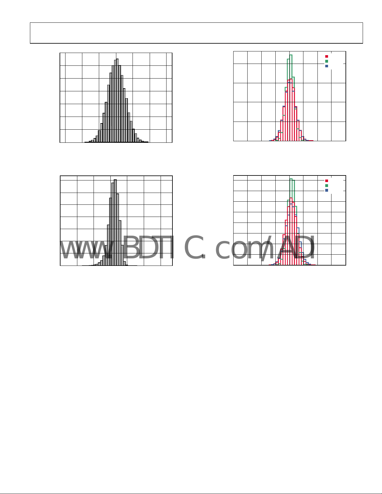
www.BDTIC.com/ADI
2100
1800
4000
+125°C
+25°C
–40°C
1500
1200
COUNT
900
600
300
0
–10 10
–9 –6 –3 0 3 6 9
V
DRIFT ( µV/°C)
OS
Figure 22. Offset Drift Distribution (μV/°C), SOIC,
T
emperature Range = −40°C to +125°C
3500
3000
2500
2000
COUNT
1500
1000
500
3000
COUNT
2000
1000
0
–1.5 –1. 0 –0.5 0 0.5 1.0 1.5
–2.0 2.0
(mV)
V
05147-034
Figure 24. Offset Distribution (μV), SOIC, V
OS
= 5 V
CM
05147-036
COUNT
4000
3500
3000
2500
2000
1500
1000
500
+125°C
+25°C
–40°C
0
020
3 6 9 12 15 18
GAIN DRIFT (ppm/°C)
05147-035
Figure 23. Gain Drift Distribution (ppm/°C), SOIC,
emperature = −40°C to +125°C
T
0
–1.5 –1. 0 –0.5 0 0.5 1.0 1.5
–2.0 2.0
(mV)
V
OS
Figure 25. Offset Distribution (μV), SOIC, V
CM
= 0 V
05147-037
Rev. A | Page 9 of 16

AD8210
www.BDTIC.com/ADI
THEORY OF OPERATION
In typical applications, the AD8210 amplifies a small differential
input voltage generated by the load current flowing through a
shunt resistor. The AD8210 rejects high common-mode voltages
(up to 65 V) and provides a ground referenced buffered output
that interfaces with an analog-to-digital converter (ADC).
Figure 26 shows a simplified schematic of the AD8210.
The AD8210 is comprised of two main blocks, a differential
a
mplifier and an instrumentation amplifier. A load current
flowing through the external shunt resistor produces a voltage
at the input terminals of the AD8210. The input terminals are
connected to the differential amplifier (A1) by R1 and R2. A1
nulls the voltage appearing across its own input terminals by
adjusting the current through R1 and R2 with Q1 and Q2.
When the input signal to the AD8210 is 0 V, the currents in R1
and R2 are equal. When the differential signal is nonzero, the
current increases through one of the resistors and decreases in
the other. The current difference is proportional to the size and
polarity of the input signal.
The differential currents through Q1 and Q2 are converted
to a differential voltage by R3 and R4. A2 is configured as an
in
instrumentation amplifier. The differential voltage is converted
into a single-ended output voltage by A2. The gain is internally
set with precision-trimmed, thin film resistors to 20 V/V.
The output reference voltage is easily adjusted by the V
and the V
to V
CC
2 pin. In a typical configuration, V
REF
while V
is centered at V
2 is connected to GND. In this case, the output
REF
/2 when the input signal is 0 V.
CC
1 is connected
REF
REF
1 pin
I
SHUNT
R
SHUNT
R1 R2
V
S
A1
Q1 Q2
R3 R4
GND
AD8210
V
1
REF
V
=(I
A2
V
REF
Figure 26. Simplified Schematic
OUT
2
SHUNT×RSHUNT
)×20
05147-004
Rev. A | Page 10 of 16

AD8210
www.BDTIC.com/ADI
MODES OF OPERATION
The AD8210 can be adjusted for unidirectional or bidirectional
operation.
UNIDIRECTIONAL OPERATION
Unidirectional operation allows the AD8210 to measure
currents through a resistive shunt in one direction. The basic
modes for unidirectional operation are ground referenced
output mode and V+ referenced output mode.
In unidirectional operation, the output can be set at the negative
ra
il (near ground) or at the positive rail (near V+) when the
differential input is 0 V. The output moves to the opposite rail
when a correct polarity differential input voltage is applied. In
this case, full scale is approximately 250 mV. The required
polarity of the differential input depends on the output voltage
setting. If the output is set at ground, the polarity needs to be
positive to move the output up (see
a
t the positive rail, the input polarity needs to be negative to
move the output down (see
Tabl e 6).
Ground Referenced Output
When using the AD8210 in this mode, both reference inputs
are tied to ground, which causes the output to sit at the negative
rail when the differential input voltage is zero (see Figure 27
a
nd Tabl e 4).
R
S
+IN –IN
GND
Figure 27. Ground Referenced Output
Table 4. V+ = 5 V
VIN (Referred to −IN) V
0 V 0.05 V
250 mV 4.9 V
Tabl e 5). If the output is set
V
S
0.1µF
AD8210
V
1
REF
G=+20
V
REF
2
OUTPUT
O
05147-005
V+ Referenced Output
This mode is set when both reference pins are tied to the
positive supply. It is typically used when the diagnostic scheme
requires detection of the amplifier and wiring before power is
applied to the load (see Figure 28 and Ta b le 5 ).
R
S
+IN –IN
V
S
AD8210
V
REF
G=+20
V
REF
GND
Figure 28. V+ Referenced Output
0.1µF
1
OUTPUT
2
05147-006
Table 5. V+ = 5 V
VIN (Referred to −IN) V
O
0 V 4.9 V
−250 mV 0.05 V
BIDIRECTIONAL OPERATION
Bidirectional operation allows the AD8210 to measure currents
through a resistive shunt in two directions. The output offset
can be set anywhere within the output range. Typically, it is set
at half scale for equal measurement range in both directions. In
some cases, however, it is set at a voltage other than half scale
when the bidirectional current is nonsymmetrical.
Table 6. V+ = 5 V, V
VIN (Referred to –IN) V
+125 mV 4.9 V
−125 mV 0.05 V
Adjusting the output can also be accomplished by applying
voltage(s) to the reference inputs.
= 2.5 V with VIN = 0 V
O
O
Rev. A | Page 11 of 16

AD8210
S
www.BDTIC.com/ADI
External Referenced Output
Tying bot h V
an output offset at the reference voltage when there is no
differential input (see Figure 29). When the input is negative
r
elative to the −IN pin, the output moves down from the
reference voltage. When the input is positive relative to the
−IN pin, the output increases.
pins together to an external reference produces
REF
R
S
+IN –IN
V
S
0.1µF
R
S
+IN –IN
AD8210
V
REF
G=+20
V
S
0.1µF
1
V
REF
0V ≤ V
≤ V
REF
OUTPUT
AD8210
V
REF
≤ V
0V ≤ V
REF
S
GND
G=+20
V
1
REF
OUTPUT
V
2
REF
Figure 29. External Reference Output
Splitting an External Reference
In this case, an external reference is divided by two with
an accuracy of approximately 0.2% by connecting one
V
pin to ground and the other V
REF
pin to the reference
REF
voltage (see Figure 30).
Note that Pin V
1 and Pin V
REF
2 are tied to internal precision
REF
resistors that connect to an internal offset node. There is no
operational difference between the pins.
For proper operation, the AD8210 output offset should not be
et with a resistor voltage divider. Any additional external
s
resistance could create a gain error. A low impedance voltage
source should be used to set the output offset of the AD8210.
V
2
REF
GND
05147-008
Figure 30. Split External Reference
Splitting the Supply
By tying one reference pin to V+ and the other to the GND pin,
the output is set at midsupply when there is no differential input
(see Figure 31). This mode is beneficial because no external
re
05147-007
ference is required to offset the output for bidirectional
current measurement. This creates a midscale offset that is
ratiometric to the supply, meaning that if the supply increases
or decreases, the output still remains at half scale. For example,
if the supply is 5.0 V, the output is at half scale or 2.5 V. If the
supply increases by 10% (to 5.5 V), the output also increases by
10% (2.75 V).
R
S
+IN –IN
V
S
AD8210
V
REF
0.1µF
1
GND
Figure 31. Split Supply
Rev. A | Page 12 of 16
G=+20
V
REF
OUTPUT
2
05147-009

AD8210
www.BDTIC.com/ADI
INPUT FILTERING
In typical applications, such as motor and solenoid current
sensing, filtering at the input of the AD8210 can be beneficial
in reducing differential noise, as well as transients and current
ripples flowing through the input shunt resistor. An input lowpass filter can be implemented as shown in
Figure 32.
The 3 dB frequency for this filter can be calculated by
f
dB3_
1
××=π2
(1)
CR
FILTERFILTER
R
SHUNT<RFILTER
R
≤ 10Ω R
FILTER
C
FILTER
+IN –IN
Adding outside components, such as R
introduces additional errors to the system. To minimize these
errors as much as possible, it is recommended that R
10 Ω or lower. By adding the R
in series with the 2 kΩ
FILTER
internal input resistors of the AD8210, a gain error is
introduced. This can be calculated by
⎛
⎜
ErrorGain
×−=
100100(%)
⎜
⎝
≤ 10Ω
FILTER
V
S
0.1µF
AD8210
and C
FILTER
k2
−
R
k2
FILTER
,
FILTER
be
FILTER
⎞
⎟
(2)
⎟
⎠
V
REF
0V ≤ V
≤ V
REF
V
1
REF
G=+20
V
2
REF
GND
Figure 32. Input Low-Pass Filtering
OUTPUT
S
05147-013
Rev. A | Page 13 of 16

AD8210
V
V
V
www.BDTIC.com/ADI
APPLICATIONS INFORMATION
The AD8210 is ideal for high-side or low-side current sensing.
Its accuracy and performance benefits applications, such as
3-phase and H-bridge motor control, solenoid control, and
power supply current monitoring.
For solenoid control, two typical circuit configurations are used:
hig
h-side current sense with a low-side switch, and high-side
current sense with a high-side switch.
HIGH-SIDE CURRENT SENSE WITH A LOW-SIDE SWITCH
In this case, the PWM control switch is ground referenced. An
inductive load (solenoid) is tied to a power supply. A resistive
shunt is placed between the switch and the load (see Figure 33).
An ad
vantage of placing the shunt on the high side is that the
entire current, including the recirculation current, can be measured because the shunt remains in the loop when the switch is
off. In addition, diagnostics can be enhanced because short circuits
to ground can be detected with the shunt on the high side.
5
INDUCTIVE
LOAD
+IN V
REF
–IN GND V
NC = NO CONNECT
Figure 33. Low-Side Switch
AD8210
BATTERY
CLAMP
DIODE
SWITCH
SHUNT
In this circuit configuration, when the switch is closed, the
common-mode voltage moves down to the negative rail. When
the switch is opened, the voltage reversal across the inductive
load causes the common-mode voltage to be held one diode
drop above the battery by the clamp diode.
HIGH-SIDE CURRENT SENSE WITH A HIGH-SIDE SWITCH
This configuration minimizes the possibility of unexpected
solenoid activation and excessive corrosion (see Figure 34). In
his case, both the switch and the shunt are on the high side.
t
When the switch is off, the battery is removed from the load,
which prevents damage from potential short circuits to ground,
while still allowing the recirculation current to be measured and
diagnostics to be preformed. Removing the power supply from
the load for the majority of the time minimizes the corrosive
effects that could be caused by the differential voltage between
the load and ground.
0.1µF
1 +VSOUT
2 NC
REF
05147-010
5
0.1µF
SWITCH
BATTERY
+IN V
SHUNT
CLAMP
DIODE
Figure 34. High-Side Switch
–IN GND V
INDUCTIVE
LOAD
1 +VSOUT
REF
AD8210
2 NC
REF
NC = NO CONNECT
05147-011
Using a high-side switch connects the battery voltage to the
load when the switch is closed. This causes the common-mode
voltage to increase to the battery voltage. In this case, when the
switch is opened, the voltage reversal across the inductive load
causes the common-mode voltage to be held one diode drop
below ground by the clamp diode.
H-BRIDGE MOTOR CONTROL
Another typical application for the AD8210 is as part of the
control loop in H-bridge motor control. In this case, the AD8210
is placed in the middle of the H-bridge (see Figure 35) so that it
c
an accurately measure current in both directions by using the
shunt available at the motor. This configuration is beneficial for
measuring the recirculation current to further enhance the
control loop diagnostics.
5
0.1µF
MOTOR
SHUNT
Figure 35. Motor Control Application
+IN V
–IN GND V
1 +VSOUT
REF
AD8210
2 NC
REF
NC = NO CONNECT
The AD8210 measures current in both directions as the H-bridge
switches and the motor changes direction. The output of the
AD8210 is configured in an external reference bidirectional
mode (see the
Modes of Operation section).
CONTROLL ER
5V
2.5V
05147-012
Rev. A | Page 14 of 16

AD8210
www.BDTIC.com/ADI
OUTLINE DIMENSIONS
5.00 (0.1968)
4.80 (0.1890)
4.00 (0.1574)
3.80 (0.1497)
0.25 (0.0098)
0.10 (0.0040)
COPLANARITY
0.10
CONTROLL ING DIMENSI ONS ARE IN MILLIMETERS; INCH DI MENSIONS
(IN PARENTHESES) ARE ROUNDED-OFF MILLIMETER EQUIVALENTS FOR
REFERENCE ONLY AND ARE NOT APPROPRI ATE FOR USE IN DES IGN.
85
1
1.27 (0.0500)
SEATING
PLANE
COMPLIANT TO JEDEC STANDARDS MS-012-A A
BSC
6.20 (0.2441)
5.80 (0.2284)
4
1.75 (0.0688)
1.35 (0.0532)
0.51 (0.0201)
0.31 (0.0122)
8°
0°
0.25 (0.0098)
0.17 (0.0067)
0.50 (0.0196)
0.25 (0.0099)
1.27 (0.0500)
0.40 (0.0157)
45°
012407-A
Figure 36. 8-Lead Standard Small Outline Package [SOIC_N]
Narrow B
ody (R-8)
Dimensions shown in millimeters and (inches)
ORDERING GUIDE
Model Temperature Range Package Description Package Option
AD8210YRZ
AD8210YRZ-REEL
AD8210YRZ-REEL7
1
Z = RoHS Compliant Part.
1
1
1
−40°C to +125°C 8-Lead SOIC_N R-8
−40°C to +125°C 8-Lead SOIC_N, 13” Tape and Reel R-8
−40°C to +125°C 8-Lead SOIC_N, 7” Tape and Reel R-8
Rev. A | Page 15 of 16

AD8210
www.BDTIC.com/ADI
NOTES
©2006–2007 Analog Devices, Inc. All rights reserved. Trademarks and
registered trademarks are the property of their respective owners.
D05147-0-4/07(A)
T
Rev. A | Page 16 of 16
TTT
 Loading...