ANALOG DEVICES AD8209 Service Manual

High Voltage,
V
FEATURES
±8000 V HBM ESD
AEC-Q100 qualified
EMI filters included
High common-mode voltage range
−2 V to +45 V operating
−24 V to +80 V survival
Buffered output voltage
Gain = 14 V/V
Low-pass filter (single-pole or two-pole)
Wide operating temperature range
8-lead MSOP: −40°C to +125°C
Excellent ac and dc performance
±1 mV voltage offset
−5 ppm/°C typical gain drift
80 dB CMRR minimum dc to 10 kHz
APPLICATIONS
High-side current sensing
Motor controls
Solenoid controls
Power management
Low-side current sensing
Diagnostic protection
Precision Difference Amplifier
AD8209
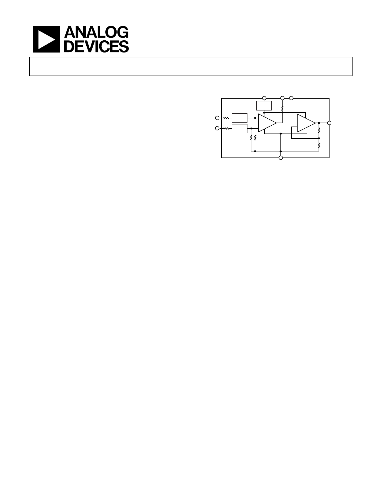
FUNCTIONAL BLOCK DIAGRAM
A1 A2
S
EMI
FILTER
IN+
IN–
EMI
FILTER
EMI
FILTER
+
–
GND
Figure 1.
+
G = 2G = 7
–
AD8209
OUT
08461-001
GENERAL DESCRIPTION
The AD8209 is a single-supply difference amplifier ideal for
amplifying and low-pass filtering small differential voltages in the
presence of a large common-mode voltage. The input commonmode voltage range extends from −2 V to +45 V at a single +5 V
supply. The AD8209 is qualified per AEC-Q100 specifications. The
amplifier offers enhanced input overvoltage and ESD protection,
and includes EMI filtering.
Automotive applications demand robust, precision components for
improved system control. The AD8209 provides excellent ac and dc
Rev. 0
Information furnished by Analog Devices is believed to be accurate and reliable. However, no
responsibility is assumed by Analog Devices for its use, nor for any infringements of patents or other
rights of third parties that may result from its use. Specifications subject to change without notice. No
license is granted by implication or otherwise under any patent or patent rights of Analog Devices.
Trademarks and registered trademarks are the property of their respective owners.
performance, minimizing errors in the application. Typical offset
and gain drift in the MSOP package are less than 5 µV/°C and
10 ppm/°C, respectively. The device also delivers a minimum
CMRR of 80 dB from dc to 10 kHz.
The AD8209 features an externally accessible 100 kΩ resistor at
the output of the preamplifier (A1), which can be used for lowpass filtering and for establishing gains other than 14.
One Technology Way, P.O. Box 9106, Norwood, MA 02062-9106, U.S.A.
Tel: 781.329.4700 www.analog.com
Fax: 781.461.3113 ©2009 Analog Devices, Inc. All rights reserved.

AD8209
TABLE OF CONTENTS
Features .............................................................................................. 1
Applications ....................................................................................... 1
Functional Block Diagram .............................................................. 1
General Description ......................................................................... 1
Revision History ............................................................................... 2
Specifications ..................................................................................... 3
Absolute Maximum Ratings ............................................................ 4
ESD Caution .................................................................................. 4
Pin Configuration and Function Descriptions ............................. 5
Typical Performance Characteristics ............................................. 6
Theory of Operation ...................................................................... 10
REVISION HISTORY
10/09—Revision 0: Initial Version
Applications Information .............................................................. 11
High-Side Current Sensing with a Low-Side Switch ............. 11
High-Rail Current Sensing ....................................................... 11
Low-Side Current Sensing ........................................................ 11
Gain Adjustment ........................................................................ 12
Gain Trim .................................................................................... 12
Low-Pass Filtering ...................................................................... 13
High Line Current Sensing with LPF and Gain Adjustment ...... 14
Outline Dimensions ....................................................................... 15
Ordering Guide .......................................................................... 15
Rev. 0 | Page 2 of 16

AD8209
SPECIFICATIONS
T
= −40°C to +125°C, TA = 25°C, VS = 5 V, RL = 25 k (RL is the output load resistor), unless otherwise noted.
OPR
Table 1.
1
Parameter Test Conditions
SYSTEM GAIN
Initial 14 V/V
Error vs. Temperature 0.075 V ≤ V
Gain Drift T
OPR
VOLTAGE OFFSET
Initial Input Offset (Referred to Input [RTI]) VCM = 0.15 V, TA ±2 mV
Input Offset (RTI) Over Temperature VCM = 0 V, T
Voltage Offset vs. Temperature VCM = 0 V, T
INPUT
Input Impedance
Differential 360 400 440 kΩ
Common Mode 180 200 220 kΩ
VCM (Continuous) −2 +45 V
2
CMRR
V
= −2 V to +45 V, dc 80 100 dB
CM
f = dc to 10 kHz,3 T
PREAMPLIFIER (A1)
Gain 7 V/V
Gain Error 0.05 V ≤ V
Output Voltage Range 0.05 VS − 0.1 V
Output Resistance 97 100 103 kΩ
OUTPUT BUFFER (A2)
Gain 2 V/V
Gain Error 0.075 V ≤ V
Output Voltage Range
Input Bias Current T
4
R
= 25 kΩ, differential Input (V) = 0 V, T
L
50 nA
OPR
Output Resistance RL = 1 kΩ, frequency = dc 2 Ω
DYNAMIC RESPONSE
System Bandwidth VIN = 0.01 V p-p, V
Slew Rate VIN = 0.28 V, V
NOISE
0.1 Hz to 10 Hz 20 μV p-p
Spectral Density, 1 kHz (RTI) 500 nV/√Hz
POWER SUPPLY
Operating Range 4.5 5.5 V
Quiescent Current Typical, TA 1.6 mA
Quiescent Current vs. Temperature V
= 0.1 V dc, VS = 5 V, T
OUT
PSRR VS = 4.5 V to 5.5 V, T
TEMPERATURE RANGE
For Specified Performance at T
1
VCM = input common-mode voltage.
2
Source imbalance < 2 Ω.
3
The AD8209 preamplifier exceeds 80 dB CMRR at 10 kHz. However, because the output is available only by way of the 100 kΩ resistor, even a small amount of pin-to-
pin capacitance between the IN pins and the A1 and A2 pins might couple an input common-mode signal larger than the greatly attenuated preamplifier output. The
effect of pin-to-pin coupling can be neglected in all applications by using a filter capacitor from Pin 3 to GND.
4
The output voltage range of the AD8209 varies depending on the load resistance and temperature. For additional information on this specification, refer to
and .
Figure 13
OPR
≤ (VS − 0.1 V), dc, T
OUT
±0.3 %
OPR
Min Typ Max Unit
0 −20 ppm/°C
±4 mV
OPR
−20 +20 μV/°C
OPR
80 dB
OPR
≤ (VS − 0.1 V), dc, T
OUT
≤ (VS − 0.1 V), dc, T
OUT
= 0.14 V p-p 80 kHz
OUT
= 4 V step 1 V/μs
OUT
OPR
66 80 dB
OPR
−0.3 +0.3 %
OPR
−0.3 +0.3 %
OPR
0.075 VS − 0.1 V
OPR
2.7 mA
−40 +125 °C
Figure 12
Rev. 0 | Page 3 of 16

AD8209
ABSOLUTE MAXIMUM RATINGS
Table 2.
Parameter Rating
Supply Voltage 12 V
Continuous Input Voltage (Common Mode) −24 V to +80 V
Differential Input Voltage ±12 V
Reversed Supply Voltage Protection 0.3 V
ESD Human Body Model ±8000 V
Operating Temperature Range −40°C to +125°C
Storage Temperature Range −65°C to +150°C
Output Short-Circuit Duration Indefinite
Lead Temperature Range (Soldering 10 sec) 300°C
Stresses above those listed under Absolute Maximum Ratings
may cause permanent damage to the device. This is a stress
rating only; functional operation of the device at these or any
other conditions above those indicated in the operational
section of this specification is not implied. Exposure to absolute
maximum rating conditions for extended periods may affect
device reliability.
ESD CAUTION
Rev. 0 | Page 4 of 16

AD8209
G
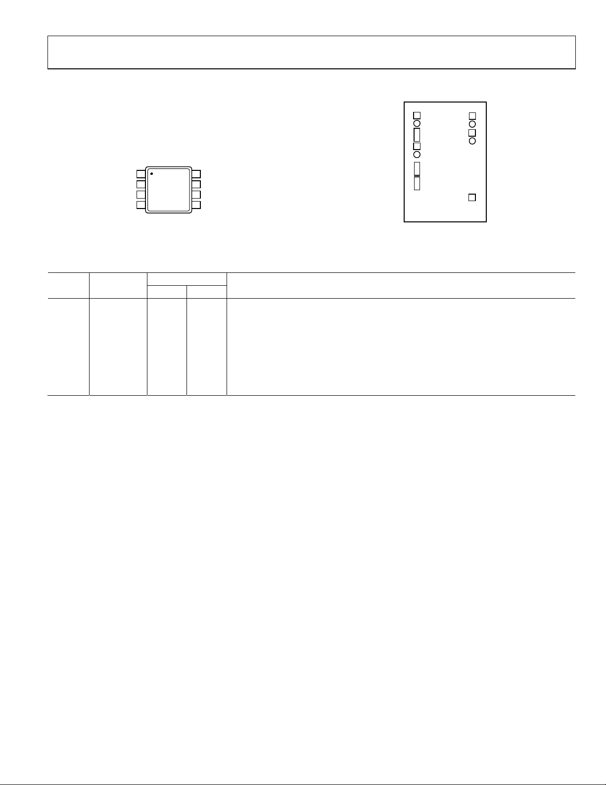
PIN CONFIGURATION AND FUNCTION DESCRIPTIONS
–IN
1
AD8209
2
ND
TOP VIEW
A1
3
(Not to Scale)
A2
4
NC = NO CONNECT
+IN
8
7
V
S
NC
6
OUT
5
08461-002
Figure 2. Pin Configuration
Table 3. Pin Function Descriptions
Coordinates
Pin No. Mnemonic X Y Description
1 −IN −322 +563 Inverting Input
2 GND −321 +208 Ground
3 A1 −321 −51 Preamplifier (A1) Output
4 A2 −321 −214 Buffer (A2) Input
5 OUT +321 −388 Buffer (A2) Output
6 NC No Connect
7 VS +322 +363 Supply
8 +IN +322 +561 Noninverting Input
1
2
3
4
8
7
5
08461-003
Figure 3. Metallization Photograph
Rev. 0 | Page 5 of 16
 Loading...