

High Voltage,
V
FEATURES
Qualified for automotive applications
EMI filters included
High common-mode voltage range
−2 V to +45 V operating
−24 V to +80 V survival
Buffered output voltage
Gain = 20 V/V
Low-pass filter (1-pole or 2-pole)
Wide operating temperature range
8-lead SOIC: −40°C to +125°C
8-lead MSOP: −40°C to +125°C
Excellent ac and dc performance
±1 mV voltage offset
−5 ppm/°C typical gain drift
80 dB CMRR minimum dc to 10 kHz
APPLICATIONS
High-side current sensing
Motor controls
Solenoid controls
Power management
Low-side current sensing
Diagnostic protection
Precision Difference Amplifier
AD8208
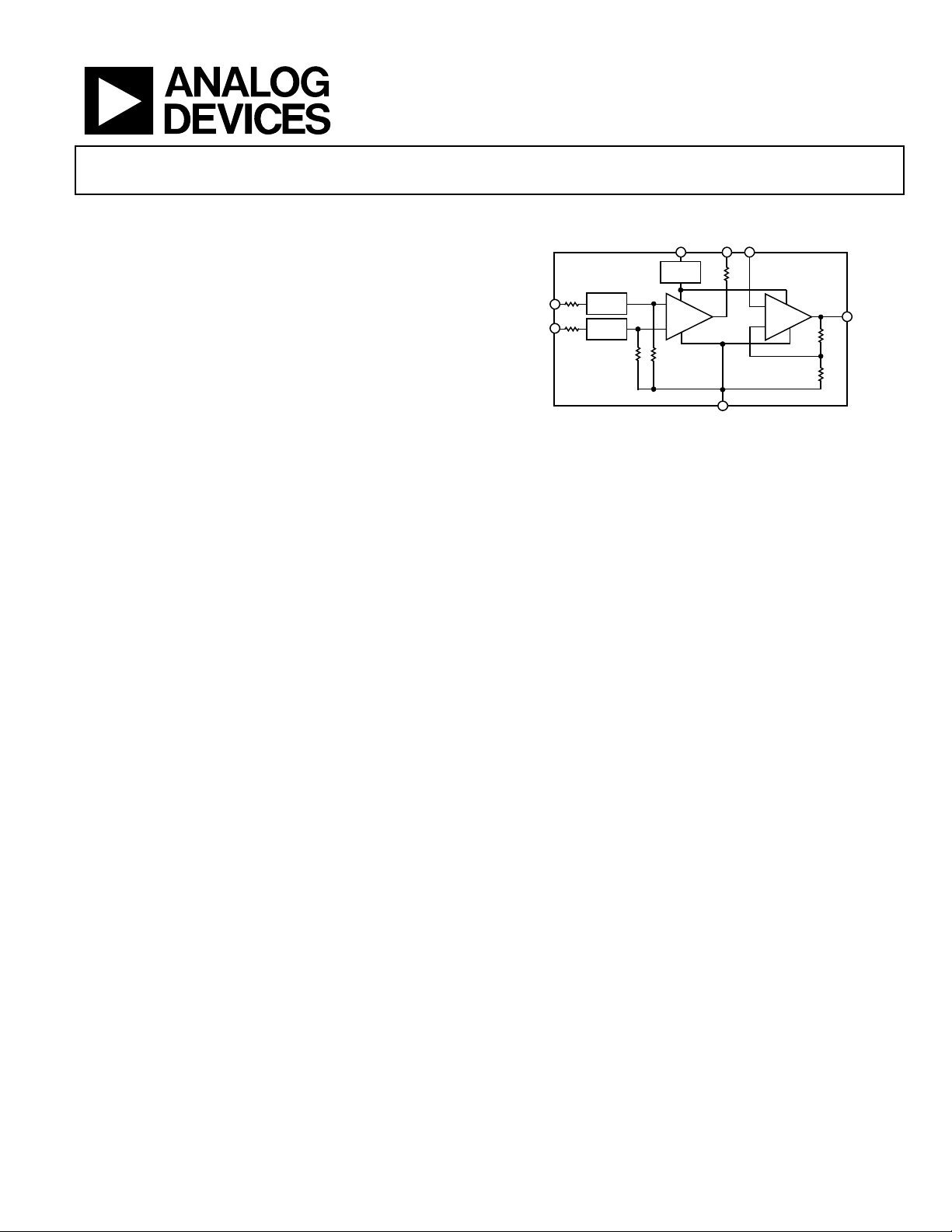
FUNCTIONAL BLOCK DIAGRAM
S
A1 A2
EMI
FILTER
+IN
–IN
EMI
FILTER
EMI
FILTER
+
–
GND
Figure 1.
+
G = 2G = 10
–
AD8208
OUT
08714-001
GENERAL DESCRIPTION
The AD8208 is a single-supply difference amplifier ideal for
amplifying and low-pass filtering small differential voltages in the
presence of a large common-mode voltage. The input commonmode voltage range extends from −2 V to +45 V at a single +5 V
supply. The AD8208 is qualified for automotive applications. The
amplifier offers enhanced input overvoltage and ESD protection,
and includes EMI filtering.
Rev. A
Information furnished by Analog Devices is believed to be accurate and reliable. However, no
responsibility is assumed by Analog Devices for its use, nor for any infringements of patents or other
rights of third parties that may result from its use. Specifications subject to change without notice. No
license is granted by implication or otherwise under any patent or patent rights of Analog Devices.
Trademarks and registered trademarks are the property of their respective owners.
Automotive applications demand robust, precision components for
improved system control. The AD8208 provides excellent ac and dc
performance, minimizing errors in the application. Typical offset
and gain drift in both the SOIC and MSOP packages are less
than 5 µV/°C and 10 ppm/°C, respectively. The device also
delivers a minimum CMRR of 80 dB from dc to 10 kHz.
The AD8208 features an externally accessible 100 kΩ resistor at
the output of the preamplifier (A1), which can be used for lowpass filtering and for establishing gains other than 20.
One Technology Way, P.O. Box 9106, Norwood, MA 02062-9106, U.S.A.
Tel: 781.329.4700 www.analog.com
Fax: 781.461.3113 ©2010 Analog Devices, Inc. All rights reserved.

AD8208
TABLE OF CONTENTS
Features .............................................................................................. 1
Applications ....................................................................................... 1
Functional Block Diagram .............................................................. 1
General Description ......................................................................... 1
Revision History ............................................................................... 2
Specifications ..................................................................................... 3
Absolute Maximum Ratings ............................................................ 4
ESD Caution .................................................................................. 4
Pin Configuration and Function Descriptions ............................. 5
Typical Performance Characteristics ............................................. 6
Theory of Operation ...................................................................... 10
REVISION HISTORY
5/10—Rev. 0 to Rev. A
Added 8-Lead MSOP ......................................................... Universal
Changes to Features Section and General Description Section . 1
Updated Outline Dimensions ....................................................... 15
Changes to Ordering Guide .......................................................... 15
1/10—Revision 0: Initial Version
Applications Information .............................................................. 11
High-Side Current Sensing with a Low-Side Switch ............. 11
High-Rail Current Sensing ....................................................... 11
Low-Side Current Sensing ........................................................ 11
Gain Adjustment ........................................................................ 12
Gain Trim .................................................................................... 12
Low-Pass Filtering ...................................................................... 13
High Line Current Sensing with LPF and Gain Adjustment ...... 14
Outline Dimensions ....................................................................... 15
Ordering Guide .......................................................................... 15
Rev. A | Page 2 of 16

AD8208
SPECIFICATIONS
T
= −40°C to +125°C, TA = 25°C, VS = 5 V, RL = 25 k (RL is the output load resistor), unless otherwise noted. Specifications applicable
OPR
for both packages (SOIC and MSOP).
Table 1.
Parameter Test Conditions1 Min Typ Max Unit
SYSTEM GAIN
Initial 20 V/V
Error vs. Temperature 0.075 V ≤ V
Gain Drift T
OPR
VOLTAGE OFFSET
Initial Input Offset (Referred to Input [RTI]) VCM = 0.15 V, TA ±2 mV
Input Offset (RTI) Over Temperature VCM = 0 V, T
Voltage Offset vs. Temperature VCM = 0 V, T
INPUT
Input Impedance
Differential 360 400 440 kΩ
Common Mode 180 200 220 kΩ
VCM (Continuous) −2 +45 V
CMRR2 V
= −2 V to +45 V, dc 80 100 dB
CM
f = dc to 10 kHz,3 T
PREAMPLIFIER (A1)
Gain 10 V/V
Gain Error 0.05 V ≤ V
Output Voltage Range 0.05 VS − 0.1 V
Output Resistance 97 100 103 kΩ
OUTPUT BUFFER (A2)
Gain 2 V/V
Gain Error 0.075 V ≤ V
Output Voltage Range4 R
Input Bias Current T
= 25 kΩ, differential Input (V) = 0 V, T
L
50 nA
OPR
Output Resistance RL = 1 kΩ, frequency = dc 2 Ω
DYNAMIC RESPONSE
System Bandwidth VIN = 0.01 V p-p, V
Slew Rate VIN = 0.28 V, V
NOISE
0.1 Hz to 10 Hz 20 μV p-p
Spectral Density, 1 kHz (RTI) 500 nV/√Hz
POWER SUPPLY
Operating Range 4.5 5.5 V
Quiescent Current Typical, TA 1.6 mA
Quiescent Current vs. Temperature V
= 0.1 V dc, VS = 5 V, T
OUT
PSRR VS = 4.5 V to 5.5 V, T
TEMPERATURE RANGE For Specified Performance at T
1
VCM = input common-mode voltage.
2
Source imbalance < 2 Ω.
3
The AD8208 preamplifier exceeds 80 dB CMRR at 10 kHz. However, because the output is available only by way of the 100 kΩ resistor, even a small amount of pin-to-
pin capacitance between the IN pins and the A1 and A2 pins might couple an input common-mode signal larger than the greatly attenuated preamplifier output. The
effect of pin-to-pin coupling can be negated in all applications by using a filter capacitor from Pin 3 to GND.
4
The output voltage range of the AD8208 varies depending on the load resistance and temperature. For additional information on this specification, see F and
Figure 13.
≤ (VS − 0.1 V), dc, T
OUT
±0.3 %
OPR
0 −20 ppm/°C
±4 mV
OPR
−20 +20 μV/°C
OPR
80 dB
OPR
≤ (VS − 0.1 V), dc, T
OUT
≤ (VS − 0.1 V), dc, T
OUT
= 0.14 V p-p 70 kHz
OUT
= 4 V step 1 V/μs
OUT
OPR
66 80 dB
OPR
−0.3 +0.3 %
OPR
−0.3 +0.3 %
OPR
0.075 VS − 0.1 V
OPR
2.7 mA
−40 +125 °C
OPR
igure 12
Rev. A | Page 3 of 16
AD8208
ABSOLUTE MAXIMUM RATINGS
Table 2.
Parameter Rating
Supply Voltage 12 V
Continuous Input Voltage (Common Mode) −24 V to +80 V
Differential Input Voltage ±12 V
Reversed Supply Voltage Protection 0.3 V
ESD Human Body Model ±4000 V
Operating Temperature Range −40°C to +125°C
Storage Temperature Range −65°C to +150°C
Output Short-Circuit Duration Indefinite
Lead Temperature Range (Soldering, 10 sec) 300°C
Stresses above those listed under Absolute Maximum Ratings
may cause permanent damage to the device. This is a stress
rating only; functional operation of the device at these or any
other conditions above those indicated in the operational
section of this specification is not implied. Exposure to absolute
maximum rating conditions for extended periods may affect
device reliability.
ESD CAUTION
Rev. A | Page 4 of 16
AD8208
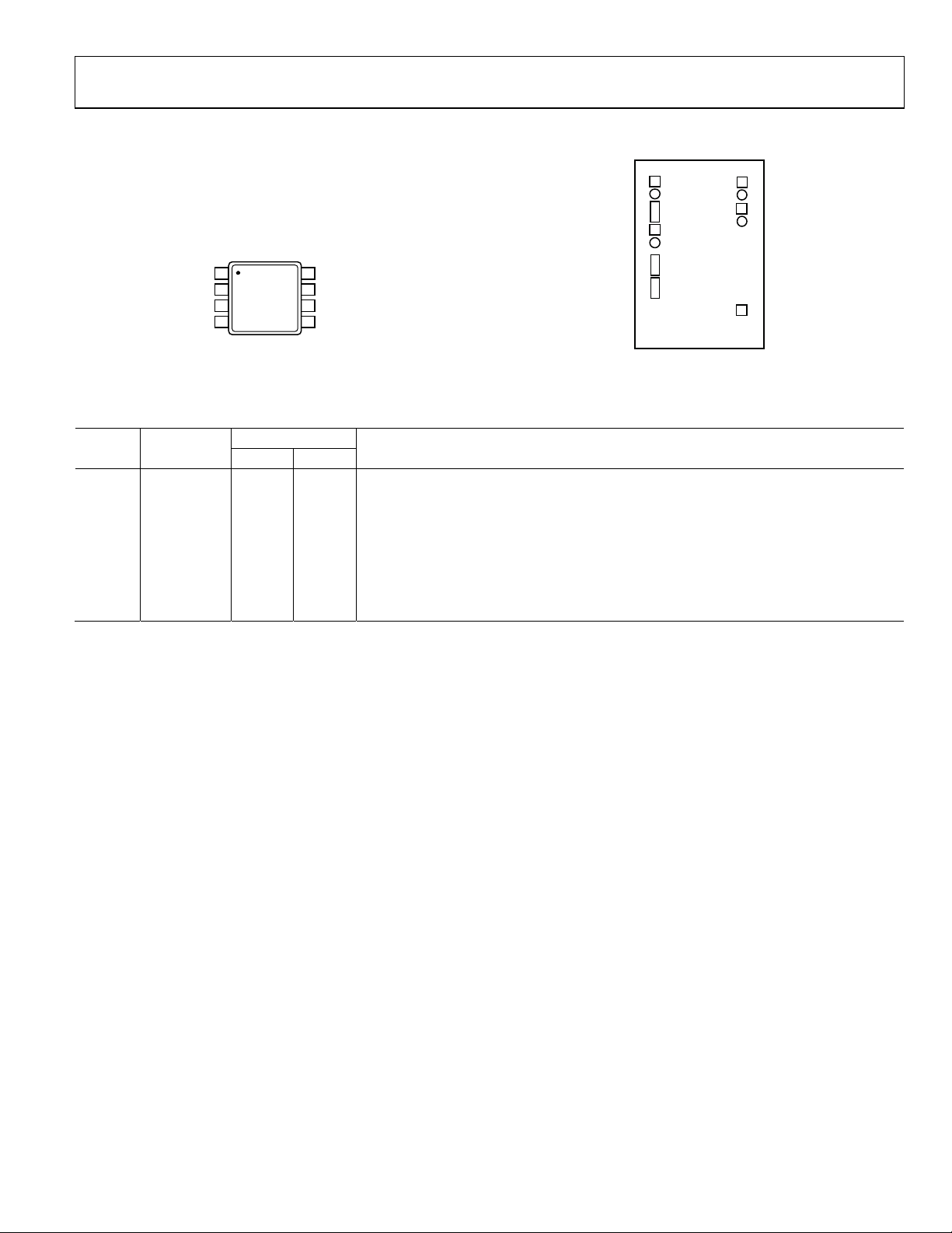
G
PIN CONFIGURATION AND FUNCTION DESCRIPTIONS
–IN
1
AD8208
2
ND
TOP VIEW
A1
3
(Not to Scale)
A2
4
NC = NO CONNECT
+IN
8
7
NC
6
V
S
OUT
5
08714-002
Figure 2. Pin Configuration
Table 3. Pin Function Descriptions
Coordinates
Pin No. Mnemonic X Y Description
1 −IN −322 +563 Inverting Input
2 GND −321 +208 Ground
3 A1 −321 −51 Preamplifier (A1) Output
4 A2 −321 −214 Buffer (A2) Input
5 OUT +321 −388 Buffer (A2) Output
6 VS +322 +363 Supply
7 NC No Connect
8 +IN +322 +561 Noninverting Input
1
2
3
4
8
6
5
08714-003
Figure 3. Metallization Photograph
Rev. A | Page 5 of 16

AD8208
–
TYPICAL PERFORMANCE CHARACTERISTICS
T
= −40°C to +125°C, TA = 25°C, VS = 5 V, RL = 25 k (RL is the output load resistor), unless otherwise noted.
OPR
0.2
1500
0.1
0
–0.1
(mV)
OSI
–0.2
V
–0.3
–0.4
–0.5
–40 –30 –20 –10 0 10 20 30 40 50 60 70 80 90 100 110120
TEMPERATURE (° C)
Figure 4. Typical Offset Drift vs. Temperature
30
25
20
15
10
5
0
GAIN (dB)
–5
–10
–15
–20
1k 10k 100k
FREQUENCY (Hz)
Figure 5. Typical Small-Signal Bandwidth
1M
1000
500
0
–500
GAIN ERROR (ppm)
–1000
–1500
–40 –25 –10 5 20 35 50 65 80 95 110 125
8714-004
TEMPERATURE (°C)
08714-007
Figure 7. Typical Gain Error vs. Temperature
0.47
0.42
0.37
0.32
0.27
0.22
0.17
0.12
0.07
TOTAL INPUT BIAS CURRENT (mA)
0.02
–0.03
–2 0 2 4 6 8 10 1214 16 18 2022 24 26 28 30 32 34 36 38 40 42 44
08714-005
INPUT COMMO N-MODE (V)
08714-008
Figure 8. Total Input Bias Current vs. Common-Mode Voltage,
with +IN and –IN Pins Connected (Shorted)
120
+125°C
+25°C
110
–40°C
100
90
80
CMRR (dB)
70
60
50
40
10 100 1k 10k 100k 1M
FREQUENCY ( Hz)
Figure 6. Typical CMRR vs. Frequency
08714-006
35
–
4
°
0
–30
–25
–20
–15
–10
–5
A2 INPUT BIAS CURRENT (nA)
0
5
0
0
.
2
5
0
.
5
0
0
.
7
5
1
.
0
0
1
.
2
5
T
V
U
I
P
N
2
A
C
2
+
°
5
C
1
+
5
2
°
C
1
.
5
0
1
.
7
2
5
.
0
0
2
.
2
5
2
.
5
0
)
(
V
E
G
A
L
T
O
Figure 9. Input Bias Current of A2 vs. Input Voltage and Temperature
08714-009
Rev. A | Page 6 of 16

AD8208
11.0
10.5
10.0
9.5
9.0
8.5
8.0
7.5
7.0
6.5
6.0
MAXIMUM OUT PUT SINK CURRENT (mA)
5.5
5.0
–40 –30 –20 –10 0 2010 30 40 6050 70 80 90 110100 120 130
TEMPERATURE (°C)
Figure 10. Maximum Output Sink Current vs. Temperature
6.1
5.8
5.5
5.2
08714-010
1.6
1.5
1.4
1.3
1.2
1.1
1.0
0.9
0.8
0.7
0.6
0.5
0.4
OUTPUT VO LTAGE RANG E (V)
0.3
0.2
0.1
0
012345678910
OUTPUT SINK CURRENT (mA)
–40°C
+25°C
+125°C
Figure 13. Output Voltage Range from GND vs. Output Sink Current
INPUT
100mV/DIV
2
OUTPUT
08714-013
4.9
4.6
4.3
MAXIMUM OUT PUT SOURCE CURRENT (mA)
4.0
–40 –20 0 20 40 60 80 100 120 140
TEMPERATURE (° C)
Figure 11. Maximum Output Source Current vs. Temperature
4.9
4.7
4.5
4.3
4.1
3.9
3.7
3.5
3.3
3.1
OUTPUT VO LTAGE RANGE (V)
2.9
2.7
2.5
0 0.5 1.0 1.5 2. 0 2.5 3. 0 3. 5 4. 0 4.5 5.0 5. 5 6.0 6.5 7. 0
OUTPUT SOURCE CURRENT (mA)
–40°C +125°C+25°C
Figure 12. Output Voltage Range of A2 vs. Output Source Current
1V/DIV
1
TIME (2µs/DIV)
08714-011
08714-014
Figure 14. Rise Time
100mV/DIV
2
1
08714-012
1V/DIV
TIME (2µs/DIV)
INPUT
OUTPUT
08714-015
Figure 15. Fall Time
Rev. A | Page 7 of 16

AD8208
2
1
INPUT
OUTPUT
TIME (2µs/DIV)
Figure 16. Differential Overload Recovery, Rising
200mV/DIV
2
2V/DIV
200mV/DIV
2V/DIV
INPUT
2V/DIV
2
0.01%/DIV
1
08714-016
TIME (20µ s/DIV)
08714-019
Figure 19. Settling Time, Falling
1200
+125°C
+25°C
–40°C
1000
800
600
COUNT
400
1
TIME (2µs/DIV)
Figure 17. Differential Overload Recovery, Falling
2
1
2V/DIV
0.01%/DIV
TIME (20µ s/DIV)
Figure 18. Settling Time, Rising
OUTPUT
200
0
08714-017
–4 –3 –2 –1 0 1 2 3 4
VOS (mV)
08714-020
Figure 20. Offset Distribution
400
350
300
250
200
COUNT
150
100
50
08714-018
0
–20 –15 –10 –5 5 10 15 200
OFFSET DRIFT (µV/°C)
08714-021
Figure 21. Offset Drift Distribution
Rev. A | Page 8 of 16

AD8208
2400
2100
1800
2400
2100
1800
+125°C
+25°C
–40°C
1500
1200
COUNT
900
600
300
0
–15 –10 –5 0
Figure 22. Gain Drift Distribution
GAIN DRIFT (ppm/°C)
5101
5
08714-022
1500
1200
COUNT
900
600
300
0
–0.3 –0. 2 –0.1 0 0.1 0.2 0.3
GAIN ERROR (%)
Figure 23. Gain Error
08714-037
Rev. A | Page 9 of 16

AD8208
V
THEORY OF OPERATION
The AD8208 is a single-supply difference amplifier typically used
to amplify a small differential voltage in the presence of rapidly
changing, high common-mode voltages.
The AD8208 consists of two amplifiers (A1 and A2), a resistor
network, a small voltage reference, and a bias circuit (not shown);
see Figure 24.
The set of input attenuators preceding A1 consists of R
R
, which feature a combined series resistance of approximately
C
, RB, and
A
400 k ± 20%. The purpose of these resistors is to attenuate the
input voltage to match the input voltage range of A1. This balanced
resistor network attenuates the common-mode signal by a ratio
of 1/14. The A1 amplifier inputs are held within the power supply
range, even as Pin 1 and Pin 8 exceed the supply or fall below the
common (ground). A reference voltage of 350 mV biases the
attenuator above ground, allowing Amplifier A1 to operate in
the presence of negative common-mode voltages.
The input resistor network also attenuates normal (differential)
mode voltages. Therefore, A1 features a gain of 140 V/V to provide
a total system gain, from ±IN to the output of A1, equal to 10
V/V, as shown in the following equation:
Gain (A1) = 1/14 (V/V) × 140(V/V) = 10 V/V
A precision trimmed, 100 k resistor is placed in series with the
output of Amplifier A1. The user has access to this resistor via
an external pin (A1). A low-pass filter can be easily implemented
by connecting A1 to A2 and placing a capacitor to ground (see
Figure 33).
The value of R
and RF2 is 10 k, providing a gain of 2 V/V for
F1
Amplifier A2. When connecting Pin A1 and Pin A2 together, the
AD8208 provides a total system gain equal to
Total Gain of (A1 + A2) (V/V) = 10 (V/V) × 2 (V/V) = 20 V/V
at the output of A2 (the OUT pin).
The ratios of R
, RB, RC, and RF are trimmed to a high level of
A
precision, allowing a typical CMRR value that exceeds 80 dB. This
performance is accomplished by laser trimming the resistor ratio
matching to better than 0.01%.
–IN
+IN
S
R
R
A
A
+
A1
R
B
R
G
R
CRF
350mV
GND
–
R
B
R
R
C
F
Figure 24. Simplified Schematic
R
FILTER
A1 A2
+
A2
–
R
M
OUT
R
F1
R
F2
08714-023
Rev. A | Page 10 of 16

AD8208
V
V
APPLICATIONS INFORMATION
HIGH-SIDE CURRENT SENSING WITH A LOW-SIDE SWITCH
In load control configurations for high-side current sensing with a
low-side switch, the PWM-controlled switch is ground referenced.
An inductive load (solenoid) connects to a power supply/battery.
A resistive shunt is placed between the switch and the load (see
Figure 25). An advantage of placing the shunt on the high side
is that the entire current, including the recirculation current, is
monitored because the shunt remains in the loop when the switch
is off. In addition, shorts to ground can be detected with the shunt
on the high side, enhancing the diagnostics of the control loop. In
this circuit configuration, when the switch is closed, the commonmode voltage moves down to near the negative rail. When the
switch is opened, the voltage reversal across the inductive load
causes the common-mode voltage to be held one diode drop
above the battery by the clamp diode.
5
CLAMP
DIODE
BATTERY
NC = NO CONNECT
+
–
In cases where a high-side switch is used for PWM control of the
load current in an application, the AD8208 can be used as shown
in Figure 26. The recirculation current through the freewheeling
diode (clamp diode) is monitored through the shunt resistor. In
this configuration, the common-mode voltage in the application
drops below GND when the FET is switched off. The AD8208
operates down to −2 V, providing an accurate current measurement.
BATTERY
+
–
CLAMP
DIODE
INDUCTIVE
LOAD
SHUNT
SWITCH
+IN
–IN
NC
AD8208
GND
Figure 25. Low-Side Switch
SWITCH
NC
+IN
SHUNT
INDUCTIVE
LOAD
–IN
AD8208
GND
OUTPUT
V
OUT
S
A1
A2
C
F
5
OUTPUT
V
OUT
S
A1
A2
C
F
08714-024
HIGH-RAIL CURRENT SENSING
In the high-rail current-sensing configuration, the shunt resistor is
referenced to the battery. High voltage is present at the inputs of
the current-sense amplifier. When the shunt is battery referenced,
the AD8208 produces a linear ground-referenced analog output.
Additionally, the AD8214 can be used to provide an overcurrent
detection signal in as little as 100 ns (see Figure 27). This feature is
useful in high current systems where fast shutdown in overcurrent
conditions is essential.
OVERCURRENT
DETECTION (<100ns)
8765
REG
–INNCGND
+INV
V
S
1234
CLAMP
DIODE
SHUNT
+IN
8
NC
7
V
S
6
OUT
5
INDUCTIVE
LOAD
5V
SWITCH
+
BATTERY
–
OUT
AD8214
NC
–IN
1
GND
2
AD8208
A1
3
A2
C
4
F
Figure 27. Battery-Referenced Shunt Resistor
LOW-SIDE CURRENT SENSING
In systems where low-side current sensing is preferable, the
AD8208 provides a simple, high accuracy, integrated solution. In
this configuration, the AD8208 rejects ground noise and offers high
input to output linearity, regardless of the differential input voltage.
INDUCTIVE
CLAMP
DIODE
SWITCH
BATTERY
NC = NO CONNECT
Figure 28. Ground-Referenced Shunt Resistor
LOAD
SHUNT
+IN
–IN
5V
V
NC
AD8208
GND
A1
OUTPUT
OUT
S
A2
C
F
08714-027
8714-026
NC = NO CONNECT
08714-025
Figure 26. High-Side Switch
Rev. A | Page 11 of 16

AD8208
V
V
V
V
4 mA to 20 mA Current Loop Receiver
The AD8208 can also be used in low current-sensing applications, such as the 4 mA to 20 mA current loop receiver shown
in Figure 29. In such applications, the relatively large shunt
resistor may degrade the common-mode rejection. Adding a
resistor of equal value on the low impedance side of the input
corrects this error.
5
10Ω
+
BATTERY
–
10Ω
1%
1%
+IN
–IN
V
NC
AD8208
GND
A1
S
OUTPUT
OUT
A2
used should be equal to 100 kΩ minus the parallel sum of R
and 100 kΩ. For example, with R
= 100 kΩ (yielding a composite
EXT
gain of 10 V/V), the optional offset nulling resistor is 50 kΩ.
Gains Greater than 20
Connecting a resistor from the output of the buffer amplifier to
its noninverting input, as shown in Figure 31, increases the gain.
The gain is now multiplied by the factor
/(R
R
EXT
For example, it is doubled for R
− 100 kΩ)
EXT
= 200 kΩ. Overall gains as
EXT
high as 50 are achievable in this way. Note that the accuracy of
the gain becomes critically dependent on the resistor value at
high gains. In addition, the effective input offset voltage at Pin 1
and Pin 8 (which is about six times the actual offset of A1) limits
the use of the part in high gain, dc-coupled applications.
5
EXT
C
F
NC = NO CONNECT
08714-028
Figure 29. 4 mA to 20 mA Current Loop Receiver
GAIN ADJUSTMENT
The default gain of the preamplifier and buffer are 10 V/V and
2 V/V, respectively, resulting in a composite gain of 20 V/V. With
the addition of external resistor(s) or trimmer(s), the gain can
be lowered, raised, or finely calibrated.
Gains Less than 20
Because the preamplifier has an output resistance of 100 kΩ, an
external resistor connected from Pin 3 and Pin 4 to GND decreases
the gain by the following factor (see Figure 30):
/(100 kΩ + R
R
EXT
V
DIFF
V
CM
+
–
+
–
+IN
–IN
)
EXT
5
V
NC
AD8208
GND
A1
OUTPUT
OUT
S
GAIN =
R
A2
R
EXT
EXT
R
EXT
= 100kΩ
20R
+ 100kΩ
EXT
GAIN
20 – GAIN
OUTPUT
+IN
+
V
DIFF
–
–IN
+
V
CM
–
NC = NO CONNECT
Figure 31. Adjusting for Gains Greater than 20
V
NC
AD8208
GND
A1
OUT
S
GAIN =
R
EXT
R
A2
EXT
R
EXT
= 100kΩ
20R
– 100kΩ
EXT
GAIN
GAIN – 20
08714-030
GAIN TRIM
Figure 32 shows a method for incremental gain trimming by
using a trim potentiometer and an external resistor, R
The following approximation is useful for small gain ranges:
G ≈ (10 MΩ ÷ R
EXT
)%
For example, using this equation, the adjustment range is ±2%
for R
= 5 MΩ and ±10% for R
EXT
+IN
+
V
DIFF
–
AD8208
NC
= 1 MΩ.
EXT
5
V
OUT
S
OUTPUT
EXT
.
NC = NO CONNECT
08714-029
Figure 30. Adjusting for Gains Less than 20
The overall bandwidth is unaffected by changes in gain by using
this method, although there may be a small offset voltage due to
+
V
CM
–
GND
–IN
A1
A2
GAIN TRIM
20kΩ MIN
R
EXT
the imbalance in source resistances at the input to the buffer. In
many cases, this can be ignored, but if desired, the offset voltage can
be nulled by inserting a resistor in series with Pin 4. The resistor
NC = NO CONNECT
Figure 32. Incremental Gain Trimming
Rev. A | Page 12 of 16
08714-031

AD8208
V
V
Internal Signal Overload Considerations
When configuring the gain for values other than 20, the maximum
input voltage with respect to the supply voltage and ground must
be considered because either the preamplifier or the output buffer
reaches its full-scale output (V
input voltages. The input of the AD8208 is limited to (V
− 0.1 V) with large differential
S
− 0.1) ÷
S
10 for overall gains of ≤10 because the preamplifier, with its
fixed gain of 10 V/V, reaches its full-scale output before the
output buffer. For gains greater than 10, the swing at the buffer
output reaches its full scale first and then limits the AD8208
input to (V
− 0.1) ÷ G, where G is the overall gain.
S
LOW-PASS FILTERING
In many transducer applications, it is necessary to filter the signal
to remove spurious high frequency components, including noise,
or to extract the mean value of a fluctuating signal with a peakto-average ratio (PAR) greater than unity. For example, a full-wave
rectified sinusoid has a PAR of 1.57, a raised cosine has a PAR
of 2, and a half-wave sinusoid has a PAR of 3.14. Signals with
large spikes may have PARs of 10 or more.
When implementing a filter, the PAR should be considered so
that the output of the AD8208 preamplifier (A1) does not clip
before A2; otherwise, the nonlinearity would be averaged and
appear as an error at the output. To avoid this error, both amplifiers
should clip at the same time. This condition is achieved when the
PAR is no greater than the gain of the second amplifier (2 for
the default configuration). For example, if a PAR of 5 is expected,
the gain of A2 should be increased to 5.
Low-pass filters can be implemented in several ways by using
the features provided by the AD8208. In the simplest case, a
single-pole filter (20 dB/decade) is formed when the output
of A1 is connected to the input of A2 via the internal 100 kΩ
resistor by tying Pin 3 to Pin 4 and adding a capacitor from this
node to ground, as shown in Figure 33. If a resistor is added
across the capacitor to lower the gain, the corner frequency
increases; therefore, gain should be calculated using the parallel
sum of the resistor and 100 kΩ.
5
If the gain is raised using a resistor, as shown in Figure 31, the
corner frequency is lowered by the same factor as the gain is raised.
Therefore, using a resistor of 200 kΩ (for which the gain would
be doubled), results in a corner frequency scaled to 0.796 Hz µF
(0.039 µF for a 20 Hz corner frequency).
5
OUTPUT
+IN
+
V
DIFF
–
–IN
+
V
CM
–
NC = NO CONNECT
Figure 34. Two-Pole, Low-Pass Filter
V
NC
AD8208
GND
A1
255kΩ
OUT
S
C
f
(Hz) = 1/C(µF)
A2
C
C
08714-033
A two-pole filter with a roll-off of 40 dB/decade can be
implemented using the connections shown in Figure 34. This
configuration is a Sallen-Key form based on a ×2 amplifier. It is
useful to remember that a two-pole filter with a corner frequency
of f
and a single-pole filter with a corner frequency of f1 have
2
the same attenuation, that is, 40 log (f
), as shown in Figure 35.
2/f1
Using the standard resistor value shown in Figure 34 and capacitors
of equal values, the corner frequency is conveniently scaled to
1 Hz µF (0.05 µF for a 20 Hz corner frequency). A maximal flat
response occurs when the resistor is lowered to 196 kΩ, scaling
the corner frequency to 1.145 Hz µF. The output offset is raised
by approximately 5 mV (equivalent to 250 µV at the input pins).
40dB/DECADE
20dB/DECADE
ATTENUATION
40log (f2/f1)
+IN
+
V
DIFF
–
–IN
+
V
CM
–
NC = NO CONNECT
V
NC
AD8208
GND
A1
OUTPUT
OUT
S
1
f
=
2πC10
5
Figure 35. Comparative Responses of Single-Pole and Two-Pole Low-Pass Filters
08714-032
A2
C
C
C IN FARADS
F
A 1-POLE FILTER, CORNER f1, AND
A 2-POLE FILTER, CORNER f
THE SAME ATTENUATION –40lo g (f
AT F REQ UE NCY f
2
f
1
2
2
/f
1
f
2
FREQUENCY
, HAVE
2/f1
)
2
f
/f
2
1
08714-034
Figure 33. Single-Pole, Low-Pass Filter Using the Internal 100 kΩ Resistor
Rev. A | Page 13 of 16

AD8208
V
HIGH LINE CURRENT SENSING WITH LPF AND GAIN ADJUSTMENT
The circuit shown in Figure 36 is similar to Figure 25, but
includes gain adjustment and low-pass filtering.
5V
CLAMP
BATTERY
NC = NO CONNECT
+
–
A power device that is either on or off controls the current in
the load. The average current is proportional to the duty cycle
of the input pulse and is sensed by a small-value resistor. The
average differential voltage across the shunt is typically 100 mV,
although its peak value is higher by an amount that depends on the
inductance of the load and the control frequency. The commonmode voltage, on the other hand, extends from roughly 1 V above
ground for the on condition to about 1.5 V above the battery
voltage in the off condition. The conduction of the clamping
INDUCTIVE
DIODE
LOAD
SHUNT
SWITCH
+IN
–IN
V
NC
AD8208
GND
A1
OUT
S
A2
V
NULL
C
Figure 36. High Line Current-Sensor Interface;
Gain = 40 V/V, Single-Pole, Low-Pass Filter
OUTPUT
4V/AMP
191kΩ
20kΩ
OS/IB
5% CALIBRATI ON RANGE
f
(Hz) = 0.767Hz/C(µ F)
C
(0.22µF FOR
f
= 3.6Hz)
C
08714-035
diode regulates the common-mode potential applied to the device.
For example, a battery spike of 20 V may result in an applied
common-mode potential of 21.5 V to the input of the devices.
To produce a full-scale output of 4 V, a gain of 40 V/V is used,
adjustable by ±5% to absorb the tolerance in the shunt. There is
sufficient headroom to allow 10% overrange (to 4.4 V). The
roughly triangular voltage across the sense resistor is averaged
by a single-pole, low-pass filter that is set with a corner frequency
of 3.6 Hz, which provides about 30 dB of attenuation at 100 Hz.
A higher rate of attenuation can be obtained by using a two-pole
filter with a corner frequency of 20 Hz, as shown in Figure 37.
Although this circuit uses two separate capacitors, the total capacitance is less than half of what is needed for the single-pole filter.
5
CLAMP
DIODE
BATTERY
NC = NO CONNE CT
+
–
INDUCTIVE
LOAD
SHUNT
SWITCH
+IN
–IN
V
NC
AD8208
GND
A1
S
127kΩ
C
OUT
A2
Figure 37. Two-Pole Low-Pass Filter
C
f
(Hz) = 1/C(µF)
C
(0.05µF FOR
432kΩ
50kΩ
f
C
OUTPUT
= 20Hz)
08714-036
Rev. A | Page 14 of 16

AD8208
OUTLINE DIMENSIONS
5.00 (0.1968)
4.80 (0.1890)
4.00 (0.1574)
3.80 (0.1497)
0.25 (0.0098)
0.10 (0.0040)
COPLANARITY
0.10
CONTROLLING DIMENSIONS ARE IN MILLIMETERS; INCH DIMENSIONS
(IN PARENTHESES) ARE ROUNDED-OFF MILLIMETER EQUIVALENTS FOR
REFERENCE ONLY AND ARE NOT APPROPRIATE FOR USE IN DESIGN.
85
1
1.27 (0.0500)
SEATING
PLANE
COMPLIANT TO JEDEC STANDARDS MS-012-AA
BSC
6.20 (0.2441)
5.80 (0.2284)
4
1.75 (0.0688)
1.35 (0.0532)
0.51 (0.0201)
0.31 (0.0122)
8°
0°
0.25 (0.0098)
0.17 (0.0067)
0.50 (0.0196)
0.25 (0.0099)
1.27 (0.0500)
0.40 (0.0157)
45°
012407-A
Figure 38. 8-Lead Standard Small Outline Package [SOIC_N]
Narrow Body
(R-8)
Dimensions shown in millimeters and (inches)
3.20
3.00
2.80
8
5
4
0.40
0.25
5.15
4.90
4.65
1.10 MAX
15° MAX
6°
0°
0.23
0.09
0.80
0.55
0.40
100709-B
3.20
3.00
2.80
PIN 1
IDENTIFIER
0.95
0.85
0.75
0.15
0.05
COPLANARITY
1
0.65 BSC
0.10
COMPLIANT TO JEDEC STANDARDS MO-187-AA
Figure 39. 8-Lead Mini Small Outline Package [MSOP]
(RM-8)
Dimensions shown in millimeters
ORDERING GUIDE
Model1 Temperature Range Package Description Package Option Branding
AD8208WBRZ −40°C to +125°C 8-Lead SOIC_N R-8
AD8208WBRZ-R7 −40°C to +125°C 8-Lead SOIC_N, 7” Tape and Reel R-8
AD8208WBRZ-RL −40°C to +125°C 8-Lead SOIC_N, 13” Tape and Reel R-8
AD8208WBRMZ −40°C to +125°C 8-Lead Mini Small Outline Package [MSOP] RM-8 Y2F
AD8208WBRMZ-R7 −40°C to +125°C 8-Lead Mini Small Outline Package [MSOP] RM-8 Y2F
AD8208WBRMZ-RL −40°C to +125°C 8-Lead Mini Small Outline Package [MSOP] RM-8 Y2F
1
Z = RoHS Compliant Part.
Rev. A | Page 15 of 16

AD8208
NOTES
©2010 Analog Devices, Inc. All rights reserved. Trademarks and
registered trademarks are the property of their respective owners.
D08714-0-5/10(A)
Rev. A | Page 16 of 16
 Loading...