

Zero-Drift, High Voltage,
FEATURES
Ideal for current shunt applications
EMI filters included
1 μV/°C maximum input offset drift
High common-mode voltage range
−4 V to +65 V operating (5 V supply)
−4 V to +35 V operating (3.3 V supply)
−25 V to +75 V survival
Gain = 20 V/V
3.3 V to 5.5 V supply range
Wide operating temperature range: −40°C to +125°C
Bidirectional current monitoring
<500 nV/°C typical offset drift
<10 ppm/°C typical gain drift
>90 dB CMRR dc to 10 kHz
Qualified for automotive applications
APPLICATIONS
High-side current sensing in
Motor control
Solenoid control
Engine management
Electric power steering
Suspension control
Vehicle dynamic control
DC-to-DC converters
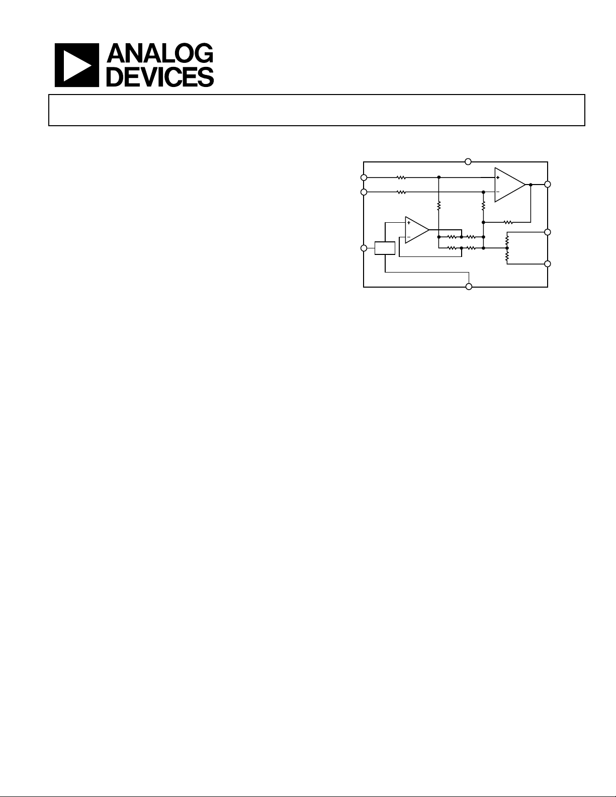
Bidirectional Difference Amplifier
AD8207
FUNCTIONAL BLOCK DIAGRAM
V+
RANGE
+IN
–IN
AD8207
REF
GND
Figure 1.
ZERO
DRIFT
OUT
V
REF
V
REF
1
2
09160-001
GENERAL DESCRIPTION
The AD8207 is a single-supply difference amplifier ideal for
amplifying small differential voltages in the presence of large
common-mode voltage. The operating input common-mode
voltage range extends from −4 V to +65 V with a 5 V supply.
The AD8207 works with a single-supply voltage of 3.3 V to 5 V,
and is ideally suited to withstand large input PWM commonmode voltages, typical in solenoid and motor control applications.
The AD8207 is available in an 8-lead SOIC package. Excellent
dc performance over temperature keeps errors in the measurement loop to a minimum. Offset drift is typically less
than 500 nV/°C, and gain drift is typically below 10 ppm/°C.
Rev. 0
Information furnished by Analog Devices is believed to be accurate and reliable. However, no
responsibility is assumed by Analog Devices for its use, nor for any infringements of patents or other
rights of third parties that may result from its use. Specifications subject to change without notice. No
license is granted by implication or otherwise under any patent or patent rights of Analog Devices.
Trademarks and registered trademarks are the property of their respective owners.
The AD8207 is ideal for bidirectional current sensing
applications. It features two reference pins,V
1 and V
REF
that allow the user to easily offset the output of the device to
any voltage within the supply range. With V
V+ pin and V
2 attached to the GND pin, the output is set at
REF
1 attached to the
REF
half scale. Attaching both pins to GND causes the output to
be unipolar, starting near ground. Attaching both pins to V+
ca
uses the output to be unipolar starting near V+. Other output
offsets are achieved by applying an external low impedance
voltage to the V
1 and V
REF
2 pins.
REF
One Technology Way, P.O. Box 9106, Norwood, MA 02062-9106, U.S.A.
Tel: 781.329.4700 www.analog.com
Fax: 781.461.3113 © 2010 Analog Devices, Inc. All rights reserved.
REF
2,

AD8207
TABLE OF CONTENTS
Features .............................................................................................. 1
Applications ....................................................................................... 1
Functional Block Diagram .............................................................. 1
General Description ......................................................................... 1
Revision History ............................................................................... 2
Specifications ..................................................................................... 3
Absolute Maximum Ratings ............................................................ 4
ESD Caution .................................................................................. 4
Pin Configuration and Function Descriptions ............................. 5
Typical Performance Characteristics ............................................. 6
Theory of Operation ...................................................................... 10
Power Supply Adjustment ............................................................. 11
3.3 V to 4.5 V Supply Operation .............................................. 11
4.5 V to 5.5 V Supply Operation .............................................. 11
Output Offset Adjustment ............................................................ 12
Unidirectional Operation .......................................................... 12
Bidirectional Operation ............................................................. 12
External Referenced Output ..................................................... 13
Splitting the Supply .................................................................... 13
Splitting an External Reference ................................................ 13
Applications Information .............................................................. 14
Motor Control ............................................................................. 14
Solenoid Control ........................................................................ 15
Outline Dimensions ....................................................................... 16
Ordering Guide .......................................................................... 16
Automotive Products ................................................................. 16
REVISION HISTORY
7/10—Revision 0: Initial Version
Rev. 0 | Page 2 of 16

AD8207
SPECIFICATIONS
T
= −40°C to +125°C, V+ = 5 V or 3.3 V, unless otherwise noted.
OPR
Table 1.
Parameter Min Typ Max Unit Test Conditions/Comments
GAIN
Initial 20 V/V
Accuracy over Temperature −0.3 +0.3 % T
Gain vs. Temperature −15 0 ppm/°C T
VOLTAGE OFFSET
Offset Voltage (RTI)1 ±100 µV 25°C
Over Temperature (RTI)1 ±400 µV T
Offset Drift −1 +1 V/°C T
INPUT
Input Impedance
Differential 240 kΩ
Common Mode 126 kΩ
Input Voltage Range −4 +65 V Common mode, continuous, V+ = 5 V, T
−4 +35 V Common mode continuous, V+ = 3.3 V, T
250 mV Differential2, V+ = 5 V
Common-Mode Rejection (CMRR) 80 90 dB T
OUTPUT
Output Voltage Range 0.02 V+ − 0.05 V RL = 25 kΩ, T
Output Resistance 2 Ω
DYNAMIC RESPONSE
Small-Signal −3 dB Bandwidth 150 kHz T
Slew Rate 1 V/µs
NOISE
0.1 Hz to 10 Hz, (RTI)1 20 µV p-p
Spectral Density, 1 kHz, (RTI)1 0.6 µV/√Hz
OFFSET ADJUSTMENT
Ratiometric Accuracy3 0.497 0.503 V/V Divider to supplies, T
Accuracy (RTO)4 ±3 mV/V
Output Offset Adjustment Range 0.02 V+ − 0.05 V T
V
Input Voltage Range
REF
5
0.0 V+ V
VREF Divider Resistor Values 100 kΩ
POWER SUPPLY
Operating Range 4.5 5.5 V RANGE (Pin 4) connected to GND
3.3 4.5 V RANGE (Pin 4) connected to V+7
Quiescent Current over Temperature 2.5 mA VO = 0.1 V dc
Power Supply Rejection Ratio (PSRR) 80 dB
TEMPERATURE RANGE
For Specified Performance −40 +125 °C
1
RTI = referred to input.
2
Input voltage range = ±125 mV with half-scale offset. The input differential range also depends on the supply voltage. The maximum input differential range can be
calculated by V+/20.
3
The offset adjustment is ratiometric to the power supply when V
4
RTO = referred to output.
5
The reference pins should be driven with a low impedance voltage source to maintain the specified accuracy of the AD8207.
6
With a 4.5 V to 5.5 V supply, the RANGE pin should be tied low. In this mode, the common-mode range of the AD8207 is −4 V to +65 V.
7
With a 3.3 V to 4.5 V supply, the RANGE pin should be tied to V+. In this mode, the common-mode range of the AD8207 is −4 V to +35 V. If a 4.5 V supply is used, the
user can tie RANGE high or low depending on the common-mode range needed in the application.
1 and V
REF
2 are used as a divider between the supplies.
REF
OPR
OPR
OPR
OPR
, f = dc to 20 kHz
OPR
OPR
OPR
Voltage applied to V
T
OPR
OPR
OPR
1 and V
REF
OPR
OPR
2 in parallel,
REF
6
Rev. 0 | Page 3 of 16
AD8207
ABSOLUTE MAXIMUM RATINGS
Table 2.
Parameter Rating
Supply Voltage 12.5 V
Continuous Input Voltage −25 V to +75 V
Input Transient Survival −30 V to +80 V
Differential Input Voltage −25 V to +75 V
Reverse Supply Voltage 0.3 V
Operating Temperature Range −40°C to +125°C
Storage Temperature Range −65°C to +150°C
Output Short-Circuit Duration Indefinite
Stresses above those listed under Absolute Maximum Ratings
may cause permanent damage to the device. This is a stress
rating only and functional operation of the device at these or
any other conditions above those indicated in the operational
section of this specification is not implied. Exposure to absolute
maximum rating conditions for extended periods may affect
device reliability.
ESD CAUTION
Rev. 0 | Page 4 of 16

AD8207
PIN CONFIGURATION AND FUNCTION DESCRIPTIONS
–IN
1
2
2
3
4
AD8207
TOP VIEW
(Not to Scale)
GND
V
REF
RANGE
Figure 2. Pin Configuration
Table 3. Pin Function Descriptions
Pin No. Mnemonic Description
1 −IN Negative Input.
2 GND Ground Pin.
3 V
2 Reference Input.
REF
4 RANGE Range Pin. This pin switches between 4.5 V to 5.5 V and 3.3 V to 4.5 V supply operation.
5 OUT Output.
6 V+ Supply Pin.
7 V
1 Reference Input.
REF
8 +IN Positive Input.
+IN
8
V
1
7
REF
V+
6
OUT
5
09160-002
Rev. 0 | Page 5 of 16

AD8207
–
TYPICAL PERFORMANCE CHARACTERISTICS
10
–12
–14
–16
–18
(µV)
–20
OSI
V
–22
–24
–26
–28
–30
–40 –20 0 20 40 60
TEMPERATURE (°C)
80 100 120 140
Figure 3. Typical Offset Drift vs. Temperature
140
130
120
110
100
CMRR (dB)
90
80
70
60
100 1k 10k 100k 1M
FREQUENCY ( Hz)
Figure 4. Typical CMRR vs. Frequency
500
400
300
200
100
0
–100
GAIN ERROR (p pm)
–200
–300
–400
–500
–40 –20 0 20 40 60 80 100 120 140
TEMPERAT URE (°C)
Figure 5. Typical Gain Error vs. Temperature
09160-003
09160-004
09160-005
40
30
20
10
0
–10
GAIN (dB)
–20
–30
–40
–50
–60
1k 10k 100k 1M 10M
Figure 6. Typical Small-Signal Bandwidth (V
FREQUENCY (Hz)
= 200 mV p-p)
OUT
19
16
13
10
7
4
TOTAL OUTPUT ERROR (%)
1
–2
0 5 10 15 20 25 30 35 40 45 50
DIFFERENTIAL INPUT VOLTAGE (mV)
Figure 7. Total Output Error vs. Differential Input Voltage
600
500
400
300
200
100
0
BIAS CURRENT PER INP UT PIN (µA)
–100
–200
–5 0 5 10 15 20 25 30 35 40 45 50 55 60 65
3.3V
5V
VCM (V)
Figure 8. Input Bias Current vs. Common-Mode Voltage
09160-006
09160-121
09160-116
Rev. 0 | Page 6 of 16

AD8207
2.0
1.8
1.6
1.4
SUPPLY CURRENT (mA)
1.2
1.0
–5 5 152535455565
5V
3.3V
INPUT COMMON-MODE VOLTAGE (V)
Figure 9. Supply Current vs. Input Common-Mode Voltage
INPUT
100mV/DIV
1
OUTPUT
1.0V/DIV
2
V+ = 3.3V
100mV/DIV
INPUT
1
1.0V/DIV
OUTPUT
V+ = 3.3V
2
09160-115
09160-009
TIME (1µs/DIV)
Figure 12. Fall Time (V+ = 3.3 V)
100mV/DIV
INPUT
1
2.0V/DIV
OUTPUT
V+ = 5V
2
1
2
TIME (1µs/DIV)
Figure 10. Rise Time (V+ = 3.3 V)
100mV/DIV
2.0V/DIV
TIME (1µs/DIV)
Figure 11. Rise Time (V+ = 5 V)
09160-007
TIME (1µs/DIV)
09160-110
Figure 13. Fall Time (V+ = 5 V)
INPUT
200mV/DIV
1
OUTPUT
V+ = 5V
09160-008
2.0V/DIV
2
INPUT
OUTPUT
V+ = 3.3V
09160-111
TIME (10µ s/DIV)
Figure 14. Differential Overload Recovery, Rising (V+ = 3.3 V)
Rev. 0 | Page 7 of 16

AD8207
INPUT
200mV/DIV
1
INPUT COMMON MODE
50V/DIV
OUTPUT
2.0V/DIV
2
TIME (10µ s/DIV)
V+ = 5V
Figure 15. Differential Overload Recovery, Rising (V+ = 5 V)
200mV/DIV
1
2.0V/DIV
2
TIME (10µ s/DIV)
INPUT
OUTPUT
V+ = 3.3V
Figure 16. Differential Overload Recovery, Falling (V+ = 3.3 V)
OUTPUT
50mV/DIV
09160-112
TIME (2µs/DIV)
09160-122
Figure 18. Input Common-Mode Step Response (V+ = 5 V, Inputs Shorted)
7.0
6.5
6.0
5.5
5.0
4.5
4.0
3.5
3.0
MAXIMUM OUT PUT SINK CURRENT (mA)
2.5
2.0
09160-113
–40 –20 0 20 40 60 80 100 120 140
5V
3.3V
09160-117
TEMPERATURE (°C)
Figure 19. Maximum Output Sink Current vs. Temperature
200mV/DIV
1
2.0V/DIV
2
TIME (10µ s/DIV)
INPUT
OUTPUT
V+ = 5V
Figure 17. Differential Overload Recovery, Falling (V+ = 5 V)
09160-114
Rev. 0 | Page 8 of 16
10
9
8
7
6
5
4
3
2
MAXIMUM OUT PUT SOURCE CURRENT (mA)
1
–40 –20 0 20 40 60 80 100 120 140
5V
3.3V
TEMPERAT URE (°C)
Figure 20. Maximum Output Source Current vs. Temperature
09160-118

AD8207
T
0
600
–100
–200
–300
–400
AGE FROM POSI TIVE RAIL (mV)
–500
VOL
–600
0 0.5 1.0 1.5 2.0 2.5 3.0 3.5 4.0 4.5 5.0
OUTPUT SOURCE CURRENT (mA)
Figure 21. Output Voltage Range vs. Output Source Current
1000
800
600
400
–40°C
500
+25°C
+125°C
400
300
COUNT
200
100
09160-120
0
–400 –200 0
OFFSET (µV)
300100–100–300
200 400
09160-023
Figure 23. Input Offset Distribution
1000
800
600
COUNT
400
200
OUTPUT VOLTAGE FROM GROUND (mV)
0
012345678
OUTPUT SI NK CURRENT (mA)
Figure 22. Output Voltage Range from GND vs. Output Sink Current
200
09160-119
0
–14 –12 –8
GAIN DRIFT (ppm/°C)
–2–6–10
–4 0
09160-024
Figure 24. Gain Drift Distribution
Rev. 0 | Page 9 of 16

AD8207
THEORY OF OPERATION
The AD8207 is a single-supply, zero drift, difference amplifier
that uses a unique architecture to accurately amplify small
differential current shunt voltages in the presence of rapidly
changing common-mode voltage.
In typical applications, the AD8207 is used to measure current
by amplifying the voltage across a shunt resistor connected to
its inputs.
The AD8207 includes a zero-drift amplifier, a precision resistor
network, a common-mode control amplifier, and a precision
reference (see Figure 25).
A set of precision-trimmed resistors make up the network
that attenuates the input common-mode voltage to within the
supply range of the amplifier, in this case with a ratio of 20/1.
This attenuation ensures that when the input pins are externally
at the common-mode extremes of −4 V and +65 V, the actual
voltage at the inputs of the main amplifier is still within the
supply range.
The input resistor network also attenuates normal (differential)
mode voltages. Therefore, the total internal gain of the AD8207
is set to 400 V/V to provide a total system gain of 20 V/V.
Total Gain (V/V) = 1/20 (V/V) × 400 (V/V) = 20 V/V
The AD8207 is designed to provide excellent common-mode
rejection, even with PWM common-mode inputs that can
change at very fast rates, for example, 1 V/ns. An internal
common-mode control amplifier is used to maintain the input
common mode of the main amplifier at 3.5 V (with 5 V supply),
and therefore eliminates the negative effects of such fastchanging external common-mode variations.
The AD8207 features an input offset drift of less than
500 nV/°C. This performance is achieved through a novel
zero-drift architecture that does not compromise bandwidth, which is typically rated at 150 kHz.
The reference inputs, V
1 and V
REF
2, are tied through 100 kΩ
REF
resistors to the positive input of the main amplifier, which
allows the output offset to be adjusted anywhere in the output
operating range. The gain is 1 V/V from the reference pins to
the output when the reference pins are used in parallel. When
the pins are used to divide the supply, the gain is 0.5 V/V.
The AD8207 offers breakthrough performance without
compromising any of the robust application needs typical
of solenoid or motor control. The part rejects PWM input
common-mode voltages, while the zero-drift architecture yields
the lowest offset and offset drift performance on the market.
SHUNT
+IN
GND
120kΩ
60kΩ
6kΩ 6kΩ
3.5V/2.2V
REF
–IN
120kΩ
100kΩ
60kΩ
100kΩ
COMMON-MO DE
CONTROL AMPLIFIER
Figure 25. Simplified Schematic
9kΩ
50kΩ
ZERO-DRIF T
AMPLIFI ER
100kΩ
100kΩ
100kΩ
AD8207
OUT
V
REF
V
REF
1
2
09160-025
Rev. 0 | Page 10 of 16

AD8207
POWER SUPPLY ADJUSTMENT
3.3 V TO 4.5 V SUPPLY OPERATION
The AD8207 can operate with a single-supply voltage as low
as 3.3 V to 4.5 V. This mode of operation is achieved by connecting the RANGE pin (Pin 4) to the supply (see Figure 26).
It is recommended that an external resistor be placed in series
from the RANGE pin to the supply. This resistor can be a
typical 5 kΩ 1% resistor.
SHUNT
4.5 V TO 5.5 V SUPPLY OPERATION
In most applications, the AD8207 operates with a single 5 V
supply. In this mode, the operating input common-mode
range of the AD8207 is rated from −4 V to +65 V. To operate
the device with a 5 V supply (includes 4.5 V to 5.5 V), connect
the RANGE pin (Pin 4) to logic low, or GND, as shown in
Figure 27.
SHUNT
3.3V
1
AD8207
2
3
TOP VIEW
(Not to Scale)
4
8
3.3V
7
6
5
OUT
09160-010
Figure 26. 3.3 V Supply Operation
Note that in this mode of operation, the common-mode range
of the AD8207 is limited to −4 V to +35 V. The output and
reference input ranges are limited to the supply of the part. The
user can have a 4.5 V supply and connect the RANGE pin from
3.3 V to 4.5 V. Alternatively, the user can connect the RANGE
pin as high as 4.5 V, with the supply from 3.3 V to 4.5 V.
1
AD8207
2
3
TOP VIEW
(Not to Scale)
4
8
7
6
5
OUT
5V
09160-011
Figure 27. 5 V Supply Bidirectional Operation
The output and reference input ranges are limited to the
supply voltage used. With a supply voltage from 4.5 V to 5.5 V,
the RANGE pin (Pin 4) should be connected to GND to achieve
the maximum input common-mode range specification of −4 V
to +65 V.
Rev. 0 | Page 11 of 16

AD8207
V
V
OUTPUT OFFSET ADJUSTMENT
The output of the AD8207 can be adjusted for unidirectional or
bidirectional operation.
UNIDIRECTIONAL OPERATION
Unidirectional operation allows the AD8207 to measure
currents through a resistive shunt in one direction. The basic
modes for unidirectional operation are ground referenced
output mode and V+ referenced output mode.
For unidirectional operation, the output can be set at the
negative rail (near ground) or at the positive rail (near V+)
when the differential input is 0 V. The output moves to the
opposite rail when a correct polarity differential input voltage
is applied. In this case, full scale is approximately 250 mV for a
5 V supply or 165 mV for a 3.3 V supply. The required polarity
of the differential input depends on the output voltage setting.
If the output is set at the positive rail, the input polarity must
be negative to move the output down. If the output is set at
ground, the polarity must be positive to move the output up.
Ground Referenced Output Mode
When using the AD8207 in the ground referenced output mode,
both reference inputs are tied to ground, which causes the output to
sit at the negative rail when there are 0 differential volts at the input
(see Figure 28).
5
V+
+IN
–IN
AD8207
ZERO
DRIFT
OUT
V+ Referenced Output Mode
The V+ referenced output mode is set when both reference pins
are tied to the positive supply. This mode is typically used when
the diagnostic scheme requires detection of the amplifier and
the wiring before power is applied to the load (see Figure 29).
5
V+
+IN
–IN
RANGE
ZERO
DRIFT
AD8207
REF
GND
Figure 29. V+ Referenced Output Mode, V+ = 5 V
OUT
V
REF
V
REF
1
2
Table 5. V+ Referenced Output
VIN (Referred to −IN) VO
V+ = 5 V
0 V 4.95 V
−250 mV 0.02 V
V+ = 3.3 V
0 V 3.25 V
−165 mV 0.02 V
09160-013
RANGE
REF
GND
Figure 28. Ground Referenced Output Mode, V+ = 5 V
Table 4. Ground Referenced Output
VIN (Referred to −IN) VO
V+ = 5 V
0 V 0.02 V
250 mV 4.95 V
V+ = 3.3 V
0 V 0.02 V
165 mV 3.25 V
1
V
REF
V
2
REF
09160-012
Rev. 0 | Page 12 of 16
BIDIRECTIONAL OPERATION
Bidirectional operation allows the AD8207 to measure currents
through a resistive shunt in two directions. In this case, the
output is set anywhere within the output range. Typically, it
is set at half scale for equal range in both directions. In some
cases, however, it is set at a voltage other than half scale when
the bidirectional current is asymmetrical.
Table 6. V
VIN (Referred to −IN) VO
V+ = 5 V
+100 mV 4.5 V
−100 mV 0.5 V
V+ = 3.3 V
+67.5 mV 3 V
−67.5 mV 0.3 V
Adjusting the output is accomplished by applying voltages
to the reference inputs. V
resistors that connect to an internal offset node. There is no
operational difference between the pins.
= (V+/2) with VIN = 0 V
O
1 and V
REF
2 are tied to internal
REF

AD8207
V
V
V
EXTERNAL REFERENCED OUTPUT
Tying both reference pins together and to an external reference
produces an output equal to the reference voltage when there is
no differential input (see Figure 30). The output moves down
from the reference voltage when the input is negative, relative
to the −IN pin, and up when the input is positive, relative to the
−IN pin. The reference pins are connected to the positive input
of the main amplifier via precision-trimmed 100 kΩ resistors.
Therefore, it is recommended that a low impedance voltage is
always be used to set the reference voltage. If external resistors
are connected directly to the V
1 and V
REF
2 pins, there will
REF
be a mismatch with the internal trimmed resistors, leading to
offset gain accuracy reduction.
5
V+
+IN
–IN
RANGE
AD8207
REF
GND
Figure 30. External Referenced Output, V+ = 5 V
ZERO
DRIFT
V
V
OUT
REF
REF
1
VOLTAGE
2.5V
REFERENCE
2
SPLITTING THE SUPPLY
By tying one reference pin to V+ and the other to the ground
pin, the output is set at half of the supply when there is no differential input (see Figure 31). The benefit is that no external
reference is required to offset the output for bidirectional current
measurement. This creates a midscale offset that is ratiometric to
the supply, which means that if the supply increases or decreases,
the output remains at half the supply. For example, if the supply is
5.0 V, the output is at half scale, or 2.5 V. If the supply increases by
10% (to 5.5 V), the output goes to 2.75 V.
5
V+
+IN
–IN
ZERO
DRIFT
OUT
AD8207
V
1
REF
RANGE
REF
GND
2
V
REF
09160-015
Figure 31. Splitting the Supply, V+ = 5 V
SPLITTING AN EXTERNAL REFERENCE
In Figure 32, an external reference is divided by 2 with an
1
5V
2
pin to
REF
VOLTAGE
REFERENCE
09160-016
accuracy of approximately 0.5% by connecting one V
ground and the other V
+IN
–IN
09160-014
RANGE
AD8207
REF
Figure 32. Splitting an External Reference, V+ = 5 V
pin to the reference (see Figure 32).
REF
5
V+
GND
ZERO
DRIFT
V
V
OUT
REF
REF
Rev. 0 | Page 13 of 16

AD8207
V
APPLICATIONS INFORMATION
MOTOR CONTROL
3-Phase Motor Control
The AD8207 is ideally suited for monitoring current in 3-phase
motor applications.
The 150 kHz typical bandwidth of the AD8207 allows for
instantaneous current monitoring. Additionally, the typical
low offset drift of 500 nV/°C means that the measurement
error between the two motor phases will be at a minimum
over temperature. The AD8207 rejects PWM input commonmode voltages in the range of −4 V to +65 V (with a 5 V
supply). Monitoring the current on the motor phase allows
for sampling of the current at any point and allows for
diagnostic information such as a short to GND and battery.
Refer to Figure 34 for a typical phase current measurement
setup with the AD8207.
H-Bridge Motor Control
Another typical application for the AD8207 is as part of
the control loop in H-bridge motor control. In this case, the
shunt resistor is placed in the middle of the H-bridge (see
Figure 33) so that it can accurately measure current in both
+
directions by using the shunt available at the motor. This is
a better solution than a ground referenced op amp because
ground is not typically a stable reference voltage in this type
of application. The instability of the ground reference causes
inaccuracies in the measurements that could be made with a
simple ground referenced op amp. The AD8207 measures
current in both directions as the H-bridge switches and the
motor changes direction. The output of the AD8207 is configured in an external referenced bidirectional mode (see the
Bidirectional Operation section).
5V
MOTOR
+IN
V
REF
OUT
+V
1
S
AD8207
SHUNT
–IN GND
V
REF
2RANGE
Figure 33. H-Bridge Motor Control Application
I
U
I
V
I
W
M
CONTROLL ER
5V
2.5V
09160-020
V–
5V 5V
AD8207
AMPLIFICATION
HIGH OUTPUT DRIVE
09160-017
AD8214
OPTIONAL
PART FOR
OVERCURRENT
PROTECTION AND
FAST (DIRECT)
SHUTDOWN OF
POWER STAGE
INTERFACE
CIRCUIT
CONTRO LLER
AD8207
REJECTION O F HIGH PW M COMMO N-MODE VOLTAGE (–4V TO +65V)
BIDIRECTIO NAL CURRENT MEASUREME NT
Figure 34. 3-Phase Motor Control
Rev. 0 | Page 14 of 16

AD8207
SOLENOID CONTROL
High-Side Current Sense with a Low-Side Switch
Other typical applications for the AD8207 include current
monitoring for PWM control of solenoid openings. Typical
applications include hydraulic valve control, diesel injection
control, and actuator control.
In Figure 35, the PWM control switch is ground referenced. An
inductive load (solenoid) is tied to a power supply. A resistive
shunt is placed between the switch and the load (see Figure 35).
An advantage of placing the shunt on the high side is that the
entire current, including the recirculation current, can be
measured because the shunt remains in the loop when the
switch is off. In addition, diagnostics capabilities are enhanced
because shorts to ground can be detected with the shunt on
the high side. In this circuit configuration, when the switch
is closed, the common-mode voltage moves down to near the
negative rail. When the switch is opened, the voltage reversal
across the inductive load causes the common-mode voltage to
be held one diode drop above the battery by the clamp diode.
V
1
REF
AD8207
5V
+V
REF
S
OUT
2 RANGE
42V
BATTERY
CLAMP
DIODE
SHUNT
SWITCH
INDUCTIVE
LOAD
+IN
–IN GND V
High-Side Current Sense with a High-Side Switch
This configuration minimizes the possibility of unexpected
solenoid activation and excessive corrosion (see Figure 36). In
Figure 36, both the switch and the shunt are on the high side.
When the switch is off, the battery is removed from the load,
which prevents damage from potential shorts to ground, while
still allowing the recirculation current to be measured and
providing for diagnostics. Removing the power supply from the
load for the majority of the time minimizes the corrosive effects
that can be caused by the differential voltage between the load
and ground. When using a high-side switch, the battery voltage
is connected to the load when the switch is closed, causing the
common-mode voltage to increase to the battery voltage. When
the switch is opened, the voltage reversal across the inductive
load causes the common-mode voltage to be held one diode
drop below ground by the clamp diode.
5V
SWITCH
OUT
+V
1
S
2 RANGE
REF
09160-019
42V
BATTERY
CLAMP
DIODE
SHUNT
+IN
–IN GND V
INDUCTIVE
LOAD
V
REF
AD8207
Figure 36. High-Side Switch
09160-018
Figure 35. Low-Side Switch
Rev. 0 | Page 15 of 16

AD8207
OUTLINE DIMENSIONS
5.00(0.1968)
4.80(0.1890)
4.00 (0.1574)
3.80 (0.1497)
0.25 (0.0098)
0.10 (0.0040)
COPLANARITY
0.10
CONTROLLING DIMENSIONS ARE IN MILLIMETERS; INCH DIMENSIONS
(IN PARENTHESES)ARE ROUNDED-OFF MILLIMETER EQUIVALENTS FOR
REFERENCE ONLYAND ARE NOT APPROPRIATE FOR USE IN DESIGN.
85
1
1.27 (0.0500)
SEATING
PLANE
COMPLIANT TO JEDEC STANDARDS MS-012-AA
BSC
6.20 (0.2441)
5.80 (0.2284)
4
1.75 (0.0688)
1.35 (0.0532)
0.51 (0.0201)
0.31 (0.0122)
8°
0°
0.25 (0.0098)
0.17 (0.0067)
0.50 (0.0196)
0.25 (0.0099)
1.27 (0.0500)
0.40 (0.0157)
45°
012407-A
Figure 37. 8-Lead Standard Small Outline Package [SOIC_N]
Narrow Body (R-8)
Dimensions shown in millimeters and (inches)
ORDERING GUIDE
1, 2
Model
AD8207WBRZ −40°C to +125°C 8-Lead SOIC_N R-8
AD8207WBRZ-R7 −40°C to +125°C 8-Lead SOIC_N, 7” Tape and Reel R-8
AD8207WBRZ-RL −40°C to +125°C 8-Lead SOIC_N, 13” Tape and Reel R-8
1
Z = RoHS Compliant Part.
2
W = Qualified for Automotive Applications.
Temperature Range Package Description Package Option
AUTOMOTIVE PRODUCTS
The AD8207 models are available with controlled manufacturing to support the quality and reliability requirements of automotive
applications. Note that these automotive models may have specifications that differ from the commercial models; therefore, designers
should review the Specifications section of this data sheet carefully. Only the automotive grade products shown are available for use in
automotive applications. Contact your local Analog Devices account representative for specific product ordering information and to
obtain the specific Automotive Reliability reports for these models.
©2010 Analog Devices, Inc. All rights reserved. Trademarks and
registered trademarks are the property of their respective owners.
D09160-0-7/10(0)
Rev. 0 | Page 16 of 16
 Loading...