

A
VCCAV
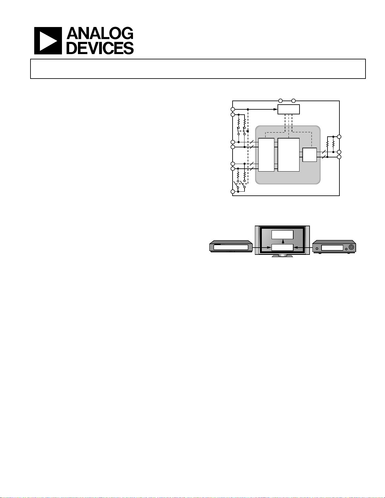
Buffered 2:1 TMDS Switch
FEATURES
2 inputs, 1 output HDMI/DVI high speed signal switch
Pin-to-pin compatible with the AD8194
Enables HDMI 1.3-compliant receiver
4 TMDS channels per input/output
Supports 250 Mbps to 2.25 Gbps data rates
Supports 25 MHz to 225 MHz pixel clocks
Fully buffered unidirectional inputs/outputs
Supports more than 20 m of input cable at 1080i, more
than 10 m of input cable at 1080p, and more than 6
meters of input cable at 1080p, 12-bit color
Matched 50 Ω input and output on-chip terminations
Low added jitter
Single-supply operation (3.3 V)
Standards compliant: HDMI receiver, DVI
32-lead, 5 mm × 5 mm, RoHS-compliant LFCSP
APPLICATIONS
Advanced television (HDTV) sets
Multiple input displays
Projectors
A/V receivers
Set-top boxes
S_SEL
VTTI
IP_A[3:0]
IN_A[3:0]
IP_B[3:0]
IN_B[3:0]
VTTI
SET-TOP BOX
AD8193
FUNCTIONAL BLOCK DIAGRAM
EE
CONTROL
LOGIC
+4
4
–
+
4
4
–
HIGH SPEED BUFFERED
SWITCH
CORE
Figure 1.
TYPICAL APPLICATION
HDTV SET
HDMI
RECEIVER
AD8193
Figure 2. Typical AD8193 Application for HDTV Sets
AD8193
TxRx
4
4
DVD PLAYER
+
–
VTTO
OP[3:0]
ON[3:0]
07003-001
07003-002
GENERAL DESCRIPTION
The AD8193 is a low cost quad 2:1 TMDS® switch for high
speed HDMI™/DVI video applications. Its primary function is
to switch the high speed signals from one of two single-link
(HDMI or DVI) sources to the single-link output. The AD8193
is a fully buffered switch solution with 50 Ω input and output
terminations, providing full-swing output signal recovery and
minimizing reflections for improved system signal integrity.
The AD8193 is provided in a space-saving, 32-lead, LFCSP,
surface-mount, RoHS-compliant, plastic package and is specified
to operate over the −40°C to +85°C temperature range.
Rev. 0
Information furnished by Analog Devices is believed to be accurate and reliable. However, no
responsibility is assumed by Anal og Devices for its use, nor for any infringements of patents or ot her
rights of third parties that may result from its use. Specifications subject to change without notice. No
license is granted by implication or otherwise under any patent or patent rights of Analog Devices.
Trademarks and registered trademarks are the property of their respective owners.
PRODUCT HIGHLIGHTS
1. Data supports rates up to 2.25 Gbps, enabling greater than
1080p deep color (12-bit color) HDMI formats and greater
than UXGA (1600 × 2300) DVI resolutions.
2. Fully buffered unidirectional inputs and outputs.
3. Supports more than 20 meters of a typical 24 AWG input
cable at 1080i, more than 10 meters at 1080p, and more
than 6 meters at 1080p, 12-bit color.
4. Matched 50 Ω on-chip input and output terminations
improve system signal integrity.
5. Single-pin source select bit.
6. Input terminations are automatically switched out for the
unselected input.
7. Low added jitter.
One Technology Way, P.O. Box 9106, Norwood, MA 02062-9106, U.S.A.
Tel: 781.329.4700 www.analog.com
Fax: 781.461.3113 ©2007 Analog Devices, Inc. All rights reserved.

AD8193
TABLE OF CONTENTS
Features.............................................................................................. 1
Applications....................................................................................... 1
Functional Block Diagram .............................................................. 1
Typical Application........................................................................... 1
General Description ......................................................................... 1
Product Highlights ........................................................................... 1
Revision History ............................................................................... 2
Specifications..................................................................................... 3
Absolute Maximum Ratings............................................................ 4
Thermal Resistance ...................................................................... 4
Maximum Power Dissipation..................................................... 4
ESD Caution.................................................................................. 4
Pin Configuration and Function Descriptions............................. 5
REVISION HISTORY
11/07—Revision 0: Initial Version
Typical Performance Characteristics..............................................6
Theory of Operation .........................................................................9
Introduction...................................................................................9
Input Channels ..............................................................................9
Output Channels........................................................................ 10
Switching Mode.......................................................................... 10
Application Notes........................................................................... 11
Switching High Speed Signals................................................... 11
Switching Low Speed Signals.................................................... 11
PCB Layout Guidelines.............................................................. 11
Outline Dimensions....................................................................... 16
Ordering Guide .......................................................................... 16
Rev. 0 | Page 2 of 16

AD8193
SPECIFICATIONS
TA = 27°C, AVCC = 3.3 V, VTTI = 3.3 V, VTTO = 3.3 V, AVEE = 0 V, differential input swing = 1000 mV, pattern = PRBS 27 − 1,
data rate = 2.25 Gbps, TMDS outputs terminated with external 50 Ω resistors to 3.3 V, unless otherwise noted.
Table 1.
Parameter Conditions/Comments Min Typ Max Unit
DYNAMIC PERFORMANCE
Maximum Data Rate (DR) per Channel NRZ 2.25 Gbps
Bit Error Rate (BER) 10−9
Added Deterministic Jitter 25 ps (p-p)
Added Random Jitter 1 ps (rms)
Differential Intrapair Skew At output 1 ps
Differential Interpair Skew
INPUT CHARACTERISTICS
Input Voltage Swing Differential 150 1200 mV
Input Common-Mode Voltage (V
OUTPUT CHARACTERISTICS
High Voltage Level Single-ended high speed channel AVCC mV
Low Voltage Level Single-ended high speed channel AVCC − 600 AVCC − 400 mV
Rise/Fall Time (20% to 80%) 75 178 ps
TERMINATION
Input Resistance Single-ended 50 Ω
Output Resistance Single-ended 50 Ω
POWER SUPPLY
AVCC Operating range 3 3.3 3.6 V
QUIESCENT CURRENT
AVCC 50 70 mA
VTTI 40 54 mA
VTTO 40 65 mA
POWER DISSIPATION
3
SOURCE SELECT INTERFACE
Input High Voltage (VIH) S_SEL 2 V
Input Low Voltage (VIL) S_SEL 0.8 V
1
Differential interpair skew is measured between the TMDS pairs of a single link.
2
Typical value assumes only the selected HDMI/DVI link is active with nominal signal swings and that the unselected HDMI/DVI link is deactivated. Minimum and
maximum limits are measured at the respective extremes of input termination resistance and input voltage swing.
3
The total power dissipation excludes power dissipated in the 50 Ω off-chip loads.
1
ICM
2
At output 30 ps
) AVCC − 800 AVCC mV
429 mW
Rev. 0 | Page 3 of 16
AD8193
ABSOLUTE MAXIMUM RATINGS
Table 2.
Parameter Rating
AVCC to AVEE 3.7 V
VTTI AVCC + 0.6 V
VTTO AVCC + 0.6 V
Internal Power Dissipation 1.2 W
High Speed Input Voltage AVCC − 1.4 V < VIN < AVCC + 0.6 V
High Speed Differential
Input Voltage
Source Select (S_SEL) AVEE − 0.3 V < VIN < AVCC + 0.6 V
Storage Temperature Range −65°C to +125°C
Operating Temperature
Range
Junction Temperature 150°C
2.0 V
−40°C to +85°C
Stresses above those listed under Absolute Maximum Ratings
may cause permanent damage to the device. This is a stress
rating only; functional operation of the device at these or any
other conditions above those indicated in the operational
section of this specification is not implied. Exposure to absolute
maximum rating conditions for extended periods may affect
device reliability.
THERMAL RESISTANCE
θJA is specified for the worst-case conditions: a device soldered
in a 4-layer JEDEC circuit board for surface-mount packages.
is specified for the exposed pad soldered to the circuit board
θ
JC
with no airflow.
Table 3. Thermal Resistance
θ
Package Type
32-Lead LFCSP 47 6.8 °C/W
θJC
JA
Unit
MAXIMUM POWER DISSIPATION
The maximum power that can be safely dissipated by the
AD8193 is limited by the associated rise in junction temperature. The maximum safe junction temperature for plastic
encapsulated devices is determined by the glass transition
temperature of the plastic, approximately 150°C. Temporarily
exceeding this limit may cause a shift in parametric performance
due to a change in the stresses exerted on the die by the package.
Exceeding a junction temperature of 175°C for an extended
period can result in device failure. To ensure proper operation,
it is necessary to observe the maximum power derating as
determined by the coefficients in
Tabl e 3.
ESD CAUTION
Rev. 0 | Page 4 of 16
AD8193
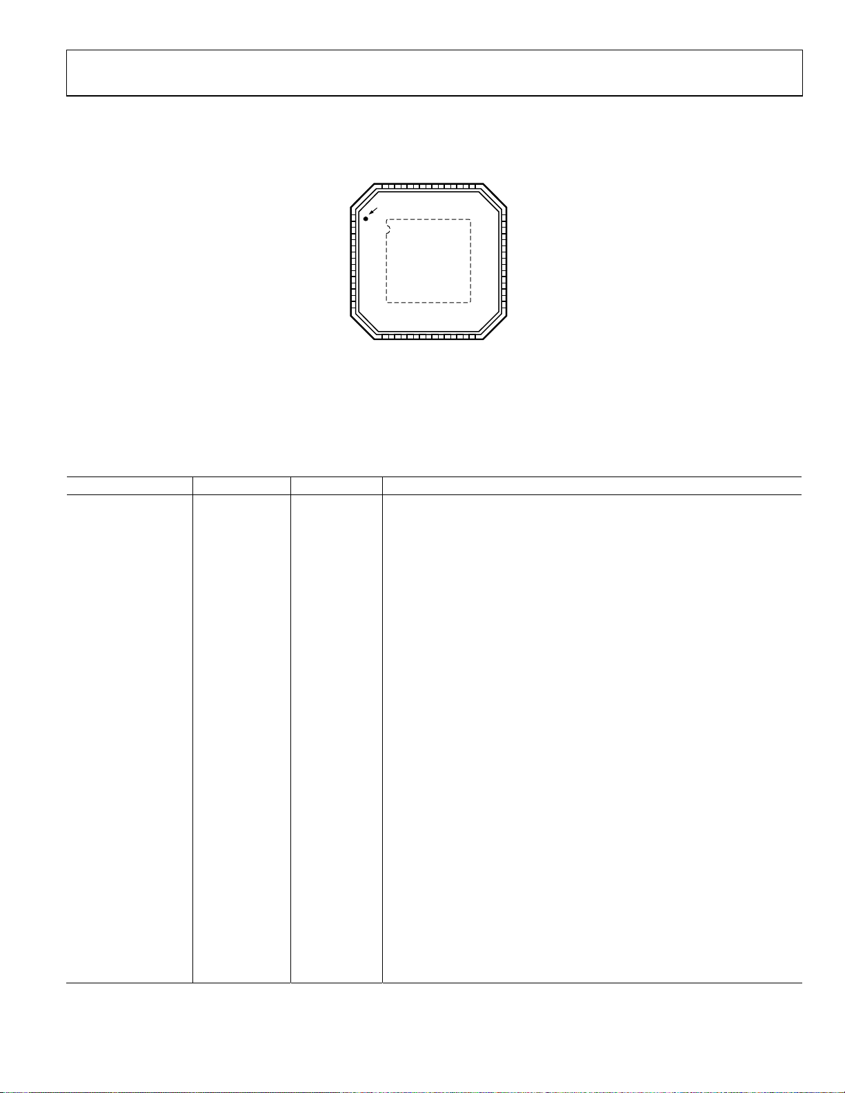
PIN CONFIGURATION AND FUNCTION DESCRIPTIONS
IP_A1
IN_A1
S_SEL
IP_A0
IN_A0
AVEE
IP_B3
32313029282726
PIN 1
IN_A2
IP_A2
VTTI
IN_A3
IP_A3
AVCC
OP3
ON3
NOTES
1. THE AD8193 LF CSP HAS AN EXPOSED PADDLE (ePAD) ON THE UNDERSIDE
OF THE P ACKAGE, WHICH AIDS IN HEAT DI SSIPATION. THE ePAD MUST BE
ELECTRICAL LY CONNECTE D TO THE AVEE SUPPLY PL ANE TO MEET
THERMAL SPECIFICATIONS.
INDICATO R
1
2
3
4
5
6
7
8
AD8193
TOP VIEW
(Not to Scale)
9
10111213141516
OP2
OP1
ON2
AVEE
Figure 3. Pin Configuration
IN_B3
25
24
IP_B2
23
IN_B2
22
AVCC
21
IP_B1
20
IN_B1
19
VTTI
18
IP_B0
17
IN_B0
OP0
ON1
ON0
VTTO
07003-003
Table 4. Pin Function Descriptions
Pin No. Mnemonic Type
1
Description
1 IN_A2 HS I High Speed Input Complement.
2 IP_A2 HS I High Speed Input.
3, 19 VTTI Power Input Termination Supply. Nominally connected to AVCC.
4 IN_A3 HS I High Speed Input Complement.
5 IP_A3 HS I High Speed Input.
6, 22 AVCC Power Positive Power Supply. 3.3 V nominal.
7 OP3 HS O High Speed Output.
8 ON3 HS O High Speed Output Complement.
9 OP2 HS O High Speed Output.
10 ON2 HS O High Speed Output Complement.
11, 27, ePAD AVEE Power Negative Power Supply. 0 V nominal.
12 OP1 HS O High Speed Output.
13 ON1 HS O High Speed Output Complement.
14 VTTO Power Output Termination Supply. Nominally connected to AVCC.
15 OP0 HS O High Speed Output.
16 ON0 HS O High Speed Output Complement.
17 IN_B0 HS I High Speed Input Complement.
18 IP_B0 HS I High Speed Input.
20 IN_B1 HS I High Speed Input Complement.
21 IP_B1 HS I High Speed Input.
23 IN_B2 HS I High Speed Input Complement.
24 IP_B2 HS I High Speed Input.
25 IN_B3 HS I High Speed Input Complement.
26 IP_B3 HS I High Speed Input.
28 IN_A0 HS I High Speed Input Complement.
29 IP_A0 HS I High Speed Input.
30 S_SEL Control Source Selector Pin.
31 IN_A1 HS I High Speed Input Complement.
32 IP_A1 HS I High Speed Input.
1
HS = high speed, I = input, O = output.
Rev. 0 | Page 5 of 16

AD8193
V
V
V
V
TYPICAL PERFORMANCE CHARACTERISTICS
TA = 27°C, AVCC = 3.3 V, VTTI = 3.3 V, VTTO = 3.3 V, AVEE = 0 V, differential input swing = 1000 mV, pattern = PRBS 27 − 1,
data rate = 2.25 Gbps, TMDS outputs terminated with external 50 Ω resistors to 3.3 V, unless otherwise noted.
HDMI CABLE
DIGITAL
PATTERN
GENERATOR
AD8193
EVALUATION
BOARD
SMA COAX CABLE
SERIAL DATA
ANALYZER
REFERENCE EYE DI AGRAM AT TP 1
TP1 TP2 TP3
7003-004
Figure 4. Test Circuit Diagram for Rx Eye Diagrams
250mV/DI
0.125UI/DI V AT 2.25Gbps
Figure 5. Rx Eye Diagram at TP2 (Cable = 2 m, 30 AWG)
07003-005
250mV/DI
0.125UI/DI V AT 2.25Gbps
Figure 7. Rx Eye Diagram at TP3 (Cable = 2 m, 30 AWG)
07003-007
250mV/DI
0.125UI/DI V AT 2.25Gbps
Figure 6. Rx Eye Diagram at TP2 (Cable = 6 m, 24 AWG)
07003-006
250mV/DI
0.125UI/DI V AT 2.25Gbps
Figure 8. Rx Eye Diagram at TP3 (Cable = 6 m, 24 AWG)
07003-008
Rev. 0 | Page 6 of 16

AD8193
TA = 27°C, AVCC = 3.3 V, VTTI = 3.3 V, VTTO = 3.3 V, AVEE = 0 V, differential input swing = 1000 mV, pattern = PRBS 27 − 1,
data rate = 2.25 Gbps, TMDS outputs terminated with external 50 Ω resistors to 3.3 V, unless otherwise noted.
0.6
2m TO 5m = 30AW G
6m = 24AWG
10m = 28AWG
0.5
20m = 24AWG
0.4
0.3
0.2
DETERMINISTIC JIT TER (UI)
0.1
1080p
12-BIT
1080p
8-BIT
1080i/720p
480p
50
40
1080p
DJ (p-p )
RJ (rms)
12-BIT
30
20
JITTER (ps)
10
480i
1080i/720p
480p
1080p
8-BIT
1.65Gbp s
0
0 5 10 15 20 25
HDMI CABLE LE NGTH (Meters)
Figure 9. Jitter vs. Input Cable Length (See
1.2
1.0
0.8
0.6
EYE HEIGHT (V)
0.4
0.2
0
0 0.20.40.60.81.01.21.41.61.82.02.22.4
DATA RATE (Gb ps)
Figure 4 for Test Setup)
Figure 10. Eye Height vs. Data Rate
0.9
0.8
0.7
0.6
0.5
0.4
EYE HEIGHT (V)
0.3
0.2
0.1
0
2.5 2.6 2.7 2.8 2.9 3.0 3.1 3.2 3.3 3.4 3.5 3.6
SUPPLY VOLTAGE (V)
Figure 11. Eye Height vs. Supply Voltage
0
0 0. 2 0.4 0.6 0.8 1.0 1.2 1.4 1.6 1.8 2. 0 2.2 2.4
07003-010
DATA RATE (Gbp s)
07003-013
Figure 12. Jitter vs. Data Rate
50
40
30
20
JITTER ( ps)
DJ (p-p)
10
0
7003-011
3.0 3.2 3.4 3.63.1 3.3 3.5
SUPPLY VOLTAGE (V)
RJ (rms)
07003-014
Figure 13. Jitter vs. Supply Voltage
50
40
30
20
JITTER ( ps)
10
0
07003-012
0.5 1.0 1.502
DIFFERENTIAL INPUT SWING (V)
DJ (p-p)
RJ (rms)
.0
07003-015
Figure 14. Jitter vs. Differential Input Swing
Rev. 0 | Page 7 of 16

AD8193
TA = 27°C, AVCC = 3.3 V, VTTI = 3.3 V, VTTO = 3.3 V, AVEE = 0 V, differential input swing = 1000 mV, pattern = PRBS 27 − 1,
data rate = 2.25 Gbps, TMDS outputs terminated with external 50 Ω resistors to 3.3 V, unless otherwise noted.
50
50
40
30
20
JITTER (ps)
DJ (p-p)
RJ (rms)
10
0
2.5 2.7 2.9 3.1 3.3 3. 5 3.7
INPUT COMMON-MODE VOLTAGE (V)
Figure 15. Jitter vs. Input Common-Mode Voltage
60
58
56
54
52
50
48
46
44
SINGLE-ENDED INPUT RESISTANCE (Ω)
42
40
–40 –15 10 35 60 85
TEMPERATURE ( °C)
Figure 16. Single-Ended Input Resistance vs. Temperature
40
30
20
JITTER ( ps)
10
0
–40 –15 10 35 60 85
07003-016
DJ (p-p)
RJ (rms)
TEMPERATURE ( °C)
07003-018
Figure 17. Jitter vs. Temperature
160
140
120
100
80
60
40
RISE/FALL TIME 20% TO 80% (ps)
20
0
07003-017
RISE TIME
FALL TIME
0 20406080100–40 –20
TEMPERATURE ( °C)
07003-019
Figure 18. Rise and Fall Time vs. Temperature
Rev. 0 | Page 8 of 16

AD8193
V
THEORY OF OPERATION
INTRODUCTION
The primary function of the AD8193 is to switch the high speed
signals from one of two (HDMI or DVI) single-link sources to
one output. Each source group consists of four differential, high
speed channels. The four high speed channels include a dataword clock and three Transition Minimized Differential Signaling
(TMDS) data channels running at 10× the data-word clock
frequency for data rates up to 2.25 Gbps. All four high speed
channels of the AD8193 are identical; that is, the pixel clock can
be run on any of the four TMDS channels. The AD8193 does
not provide switching of the low speed DDC and CEC signals.
The AD8193 is a buffered TMDS switch with low added jitter;
the output pins are electrically isolated from the inputs. Because
the AD8193 is a TMDS-only switch, a complete HDMI switch
solution requires another component to switch the low speed
DDC channels. Several low cost CMOS switches can be used
along with the AD8193 to make an HDMI 1.3-compliant 2:1
link switch. The requirements for such a switch are as follows:
• Low input capacitance. The HDMI 1.3 specification limits
the total DDC link capacitance for an HDMI sink to less
than 50 pF. This 50 pF limit includes the HDMI connector,
the PCB, the capacitance of the CMOS switch, and whatever capacitance is seen at the input of the HDMI receiver.
• Low channel on resistance (R
resistance degrade the quality of the DDC signals.
• An appropriate form factor to switch the DDC and HPD
signals as necessary.
A reference design that incorporates the AD8193 and a low cost
CMOS switch is described in more detail in the
Board
section.
In addition to the AD8193, Analog Devices, Inc., offers several
HDMI switches with integrated DDC, in a variety of form
factors.
). Switches with high on
ON
Evaluation
INPUT CHANNELS
Each high speed input differential pair terminates to the
3.3 V VTTI power supply through a pair of single-ended 50 Ω
on-chip resistors, as shown in
chip terminations absorb reflections on the input TMDS
channels, properly terminating the inputs and improving
overall system signal integrity.
The input termination resistors all have series switches, as
shown in
Figure 19. The state of these switches is determined by
the S_SEL signal, which also controls the input selection. The
termination switches for the selected input channel are closed
(terminations present), whereas the termination switches for
the unselected input are open (high-Z inputs).
No specific cable length is suggested for use with the AD8193
because cable performance varies widely between manufacturers. For a 24 AWG reference cable, the AD8193 can operate
with more than 20 m of input cable at data rates equivalent to
1080i, more than 10 meters at 1080p, and more than 6 meters at
1080p, 12-bit color.
IP_xx
IN_xx
AVEE
Figure 19. High Speed Input Simplified Schematic
Figure 19. These matched on-
TTI
50Ω50Ω
Rx
07003-020
Rev. 0 | Page 9 of 16

AD8193
V
OUTPUT CHANNELS
Each high speed output differential pair is terminated to the
3.3 V VTTO power supply through two single-ended 50 Ω
on-chip resistors, as shown in
chip back-terminations absorb reflections on the output TMDS
channels and improve the overall system signal integrity. These
termination resistors are always present in the outputs and they
cannot be switched out.
OP[3:0] ON[3:0]
Figure 20. High Speed Output Simplified Schematic
In a typical application, the AD8193 output is connected to the
input of an HDMI/DVI receiver, which provides a second set of
matched terminations in accordance with the HDMI 1.3
specification. If no receiver is connected, each of the AD8193
output pins should be tied to 3.3 V through a 50 Ω on-board
termination resistor.
Figure 20. These matched on-
TTO
AVEE
I
50Ω
OUT
07003-021
50Ω
SWITCHING MODE
The source selector pin, S_SEL, is used to select which of the
two input groups is routed to the output. Source A is selected
when S_SEL is pulled up to logic high, and Source B is selected
when S_SEL is pulled down to logic low. Logic levels for this pin
are set in accordance with the specifications listed in
AD8193 can be used as a single-link TMDS buffer by setting
S_SEL to one fixed logic value.
S_SEL also controls the switch status of the input termination
resistors. The termination resistors for the selected input are
always connected, whereas the termination resistors for the
unselected input are always switched out (high-Z inputs).
Table 5. S_SEL Description
Selected
S_SEL
Input
0 Input B
Input Termination Status
Input B terminations enabled, Input A
terminations disabled
1 Input A
Input A terminations enabled, Input B
terminations disabled
Table 5 . The
Rev. 0 | Page 10 of 16

AD8193
APPLICATION NOTES
SWITCHING HIGH SPEED SIGNALS
The AD8193 is a quad 2:1 TMDS switch that is used to switch
the high speed signals of two input HDMI links to a single
HDMI output.
SWITCHING LOW SPEED SIGNALS
Because the AD8193 is a TMDS-only switch, a complete HDMI
switch solution requires another component to switch the low
speed DDC channels.
The HDMI 1.3 specification places a number of restrictions on
the low speed signal path that limit the selection of a suitable
low cost DDC switch. The first requirement is that the switch
must be bidirectional to convey the I
2
C® protocol signals that
pass through it. A CMOS device is the simplest switch with this
capability.
The second HDMI requirement for the DDC signals is that the
total DDC signal path capacitance be less than 50 pF. The total
capacitance comprises the HDMI connector, the PC board
traces, the DDC switch, and the input capacitance of the HDMI
receiver. As a practical design consideration, a suitable DDC
switch has a total channel capacitance of less than 10 pF.
Finally, the channel on resistance (R
) of the DDC switch must
ON
not be too high, otherwise the voltage drop across it violates the
maximum V
of the I2C signals. Any switch with an on resistance
OL
of approximately 100 is sufficient in a typical application, assuming that the end application includes an I
2
C-compliant receiver
device. Switches with lower channel on resistance have improved
V
performance.
OL
For the AD8193 evaluation board, the MC74LVX4053 was
chosen to switch the low speed signals. This part has a maximum
R
of 108 and a maximum parasitic capacitance of 10 pF.
ON
Refer to the
Evaluation Board section for details on how to use
the MC74LVX4053 with the AD8193 in an application.
PCB LAYOUT GUIDELINES
The AD8193 is used to switch HDMI/DVI video signals, which
are differential, unidirectional, and high speed (up to 2.25 Gbps).
The channels that carry the video data must be controlled
impedance, terminated at the receiver, and capable of operating
up to at least 2.25 Gbps. It is especially important to note that
the differential traces that carry the TMDS signals should be
designed with a controlled differential impedance of 100 Ω.
The AD8193 provides single-ended 50 Ω terminations on chip
for both its inputs and outputs. Transmitter termination is not
fully specified by the HDMI standard, but the inclusion of the
50 Ω output terminations improves the overall system signal
integrity.
TMDS Signals
The audiovisual (AV) data carried on these high speed channels
is encoded by a technique called Transition Minimized Differential
Signaling (TMDS) and, in the case of HDMI, is also encrypted
according to the high bandwidth digital content protection
(HDCP) standard.
In the HDMI/DVI standard, four differential pairs carry the
TMDS signals. For DVI, three of these pairs are dedicated to
carrying RGB video and sync data. For HDMI, audio data is
also interleaved with the video data; the DVI standard does
not incorporate audio information. The fourth high speed
differential pair is used for the AV data-word clock and runs
at one-tenth the speed of the TMDS data channels.
The four high speed channels of the AD8193 are identical.
No concession was made to lower the bandwidth of the fourth
channel for the pixel clock, so any channel can be used for any
TMDS signal. The user chooses which signal is routed over which
channel. Additionally, the TMDS channels are symmetrical; therefore, the p and n of a given differential pair are interchangeable,
provided the inversion is consistent across all inputs and outputs of
the AD8193. However, the routing between inputs and outputs
through the AD8193 is fixed. For example, Output Channel 0
always switches between Input A0 and Input B0, and so forth.
The AD8193 buffers the TMDS signals, and the input traces can
be considered electrically independent of the output traces. In
most applications, the quality of the signal on the input TMDS
traces is more sensitive to the PCB layout. Regardless of the data
being carried on a specific TMDS channel, or whether the
TMDS line is at the input or the output of the AD8193, all four
high speed signals should be routed on a PCB in accordance
with the same RF layout guidelines.
Layout for the TMDS Signals
The TMDS differential pairs can be either microstrip traces,
routed on the outer layer of a board, or stripline traces, routed
on an internal layer of the board. If microstrip traces are used,
there should be a continuous reference plane on the PCB layer
directly below the traces. If stripline traces are used, they must
be sandwiched between two continuous reference planes in the
PCB stackup. Additionally, the p and n of each differential pair
must have a controlled differential impedance of 100 Ω. The
characteristic impedance of a differential pair is a function of
several variables, including the trace width, the distance separating
the two traces, the spacing between the traces and the reference
plane, and the dielectric constant of the PC board binder material.
Interlayer vias introduce impedance discontinuities that can
cause reflections and jitter on the signal path; therefore, it is
preferable to route the TMDS lines exclusively on one layer of the
board, particularly for the input traces. Additionally, to prevent
unwanted signal coupling and interference, route the TMDS
signals away from other signals and noise sources on the PCB.
Rev. 0 | Page 11 of 16

AD8193
Both traces of a given differential pair must be equal in length
to minimize intrapair skew. Maintaining the physical symmetry
of a differential pair is integral to ensuring its signal integrity;
excessive intrapair skew can introduce jitter through duty
cycle distortion (DCD). The p and n of a given differential pair
should always be routed together to establish the required 100 Ω
differential impedance. Enough space should be left between
the differential pairs of a given group so that the n of one pair
does not couple to the p of another pair. For example, one technique is to make the interpair distance 4 to 10 times wider than
the intrapair spacing.
Any group of four TMDS channels (Input A, Input B, or the
output) should have closely matched trace lengths to minimize
interpair skew. Severe interpair skew can cause the data on the
four different channels of a group to arrive out of alignment
with one another. A good practice is to match the trace lengths
for a given group of four channels to within 0.05 inches on FR4
material.
The length of the TMDS traces should be minimized to reduce
overall signal degradation. Commonly used PC board material
such as FR4 is lossy at high frequencies; therefore, long traces
on the circuit board increase signal attenuation, resulting in
decreased signal swing and increased jitter through intersymbol
interference (ISI).
Controlling the Characteristic Impedance of a TMDS Differential Pair
The characteristic impedance of a differential pair depends on a
number of variables, including the trace width, the distance
between the two traces, the height of the dielectric material
between the trace and the reference plane below it, and the
dielectric constant of the PCB binder material. To a lesser
extent, the characteristic impedance also depends upon the
trace thickness and the presence of solder mask.
There are many combinations that can produce the correct
characteristic impedance. It is generally required to work with
the PC board fabricator to obtain a set of parameters to produce
the desired results.
To guarantee a differential pair with a differential impedance of
100 Ω over the entire length of the trace, change the width of
the traces in a differential pair based on how closely one trace is
coupled to the other. When the two traces of a differential pair
are close and strongly coupled, they should have a width that
produces a 100 Ω differential impedance. When the traces split
apart to go into a connector, for example, and are no longer so
strongly coupled, the width of the traces should be increased to
yield a differential impedance of 100 Ω in the new configuration.
Ground Current Return
In some applications, it may be necessary to invert the output
pin order of the AD8193. This requires routing the TMDS
traces on multiple layers of the PCB. When routing differential
pairs on multiple layers, it is also necessary to reroute the
corresponding reference plane to provide one continuous
ground current return path for the differential signals. Standard
plated through-hole vias are acceptable for both the TMDS
traces and the reference plane. An example of this is illustrated
in
Figure 21.
THROUGH-HOL E VIAS
SILKSCREEN
LAYER 1: SIG NAL (MICRO STRIP)
PCB DIELECTRI C
LAYER 2: GND (REFERENCE PLANE)
PCB DIELECTRI C
LAYER 3: PWR
(REFERENCE PLANE)
PCB DIELECTRI C
LAYER 4: SIG NAL (MICRO STRIP)
SILKSCREEN
KEEP REFERENCE P LANE
ADJACENT TO SI GNAL ON AL L
LAYERS TO PROVIDE CONTINUOUS
GROUND CURRENT RET URN PATH.
Figure 21. Example Routing of Reference Plane
TMDS Terminations
The AD8193 provides internal 50 Ω single-ended terminations
for all of its high speed inputs and outputs. The termination
resistors back-terminate the output TMDS transmission lines.
These back-terminations act to absorb reflections from impedance discontinuities on the output traces, improving the signal
integrity of the output traces and adding flexibility to how the
output traces can be routed. For example, interlayer vias can be
used to route the AD8193 TMDS outputs on multiple layers of the
PCB without severely degrading the quality of the output signal.
In a typical application, the AD8193 output is connected to an
HDMI/DVI receiver or to another device with a 50 Ω single-ended
input termination. It is recommended that the outputs be
terminated with external 50 Ω on-board resistors when the
AD8193 is not connected to another device.
07003-022
Rev. 0 | Page 12 of 16

AD8193
Auxiliary Control Signals
There are four single-ended control signals associated with each
source or sink in an HDMI/DVI application. These are hot plug
detect (HPD), consumer electronics control (CEC), and two
display data channel (DDC) lines. The two signals on the DDC
bus are SDA and SCL (serial data and serial clock, respectively).
The AD8193, which is a low cost part, does not have any
additional capability to switch these signals; other means are
required to switch these signals if required.
In general, it is sufficient to route each auxiliary signal as a
single-ended trace. These signals are not sensitive to impedance
discontinuities, do not require a reference plane, and can be
routed on multiple layers of the PCB. However, it is best to
follow strict layout practices whenever possible to prevent the
PCB design from affecting the overall application. The specific
routing of the HPD, CEC, and DDC lines depends upon the
application in which the AD8193 is being used.
For example, the maximum speed of signals present on the
auxiliary lines is 100 kHz I
any layout that enables 100 kHz I
2
C data on the DDC lines; therefore,
2
C to be passed over the DDC
bus should suffice. The HDMI 1.3 specification, however, places
a strict 50 pF limit on the amount of capacitance that can be
measured on either SDA or SCL at the HDMI input connector.
This 50 pF limit includes the HDMI connector, the PCB, the
capacitance of the CMOS switch, and whatever capacitance is
seen at the input of the HDMI receiver. There is a similar limit
of 100 pF of input capacitance for the CEC line.
The parasitic capacitance of traces on a PCB increases with
trace length. To help ensure that a design satisfies the HDMI
specification, the length of the CEC and DDC lines on the PCB
should be made as short as possible. Additionally, if there is a
reference plane in the layer adjacent to the auxiliary traces in
the PCB stackup, relieving or clearing out this reference plane
immediately under the auxiliary traces significantly decreases
the amount of parasitic trace capacitance. An example of the
board stackup is shown in
Figure 22.
W3W 3W
HPD is a dc signal presented by a sink to a source to indicate
that the source EDID is available for reading. The placement
of this signal is not critical, but it should be routed as directly
as possible.
Power Supplies
The AD8193 has three separate power supplies referenced to
a single ground. The supply/ground pairs are
• AVC C / AVE E
• VTTI/AVEE
• VTTO/AVEE
The AVCC/AVEE (3.3 V) supply powers the core of the
AD8193. The VTTI/AVEE supply (3.3 V) powers the input
termination (see
supply (3.3 V) powers the output termination (see
Figure 19). Similarly, the VTTO/AVEE
Figure 20).
In a typical application, all pins labeled AVEE should be connected directly to ground. All pins labeled AVCC, VTTI, or
VTTO should be connected to 3.3 V. The supplies can also be
powered individually, but care must be taken to ensure that
each stage of the AD8193 is powered correctly.
Power Supply Bypassing
The AD8193 requires minimal supply bypassing. When
powering the supplies individually, place a 0.01 F capacitor
between each 3.3 V supply pin (AVCC, VTTI, and VTTO) and
ground to filter out supply noise. Generally, bypass capacitors
should be placed near the power pins and should connect directly
to the relevant supplies (without long intervening traces). For
example, to minimize the parasitic inductance of the power
supply decoupling capacitors, minimize the trace length between
capacitor landing pads and the vias as shown in
RECOMMENDED
EXTRA ADDED INDUCTANCE
Figure 23.
SILKSCREEN
LAYER 1: SIGNAL (MICROSTRIP)
PCB DIEL ECTRI C
LAYER 2: GND (REFERENCE PLANE)
PCB DIEL ECTRI C
LAYER 3: PWR (REFERENCE PLANE)
PCB DIEL ECTRI C
LAYER 4: SIGNAL (MICROSTRIP)
SILKSCREEN
Figure 22. Example Board Stackup
REFERENCE LAYER
RELIEVED UNDERNEAT H
MICROSTRIP
07003-023
Rev. 0 | Page 13 of 16
NOT RECOMMENDED
Figure 23. Recommended Pad Outline for Bypass Capacitors
In applications where the AD8193 is powered by a single 3.3 V
supply, it is recommended to use two reference supply planes
and bypass the 3.3 V reference plane to the ground reference
plane with one 220 pF, one 1000 pF, two 0.01 F, and one 4.7 F
capacitors. The capacitors should via down directly to the supply
planes and be placed within a few centimeters of the AD8193.
07003-024

AD8193
Evaluation Board
The AD8193 evaluation board illustrates one way to implement
a 2:1 HDMI link switch with an AD8193 and a CMOS switch.
The AD8193 evaluation board deviates from a typical application in that it uses an HDMI connector for the output as well as
for the inputs. This setup makes it easy to connect equipment to
the AD8193 evaluation board with standard HDMI cables.
19
HDMI
CONNECTOR
However, this arrangement requires crossing over the TMDS
signals on the output side (see
Figure 24).
In a typical application, the output of the AD8193 is routed
directly into an HDMI receiver. Because a receiver is generally
designed to interface directly to an HDMI input connector, it is
not necessary to cross over the TMDS signals in a typical
application (see
CROSSOVER
REQUIRED
Figure 25).
1
HDMI
CONNECTOR
1
AD8193
19
1
CONNECTOR
19
HDMI
07003-025
Figure 24. Block Diagram of AD8193 Evaluation Board Showing Output Crossover
19
HDMI
CONNECTOR
1
AD8193
Figure 25. HDMI Signals to HDMI Receiver, No Crossover Required
HDMI
RECEIVER
07003-026
Rev. 0 | Page 14 of 16

AD8193
Figure 26 shows the layout of the TMDS traces. These are 100 Ω
differential, controlled-impedance traces. Serpentine traces are
used for some of the paths to match the lengths within a group
of four. The gray traces are routed on the top layer and the black
traces on the bottom layer.
The low speed switching is performed by an MC74LVX4053.
This part contributes a maximum on resistance of 108 and a
maximum capacitive load of 10 pF. The same select signal
(S_SEL) controls both the AD8193 and the MC74LVX4053.
07003-027
Figure 26. Layout of TMDS Traces
Rev. 0 | Page 15 of 16

AD8193
OUTLINE DIMENSIONS
INDICATOR
1.00
0.85
0.80
SEATING
PLANE
PIN 1
12° MAX
5.00
BSC SQ
TOP
VIEW
0.80 MAX
0.65 TYP
0.30
0.25
0.18
4.75
BSC SQ
0.20 REF
0.05 MAX
0.02 NOM
0.60 MAX
0.50
BSC
0.50
0.40
0.30
COPLANARITY
0.08
0.60 MAX
25
24
*
EXPOSED
(BOTTOM VIEW)
17
16
3.50 REF
PAD
PIN 1
32
9
INDICATOR
1
2.85
2.70 SQ
2.55
8
0.20 MIN
ORDERING GUIDE
Model
AD8193ACPZ
AD8193ACPZ-R7
AD8193-EVALZ
1
Z = RoHS Compliant Part.
1
1
1
*
THE AD8193 HAS A CONDUCTIVE HEAT SLUG TO HELP DISSIPATE HEAT AND ENSURE RELIABLE OPER ATION OF
THE DEVICE O VER THE FULL HDMI/DVI TEMPERATURE RANGE. THE SLUG I S EXPOSED ON THE BOTTOM OF
THE PACKAGE AND ELECTRICAL LY CONNECTED TO AVEE. IT IS RECOMM ENDED THAT NO PCB SIGNAL TRACES
OR VIAS BE LOCATED UNDER THE PACKAGE THAT COULD COME I N CONTACT WITH THE CONDUCTIVE SLUG.
ATTACHING THE SL UG TO AN AVEE PLANE REDUCES THE JUNCTION T EMPERATURE OF THE DEVICE WHICH MAY
BE BENEFICIAL IN HIGH TE MPERATURE ENVIRONMENTS.
COMPLIANT TO JEDEC STANDARDS MO-220-VHHD-2
102407-A
Figure 27. 32-Lead Lead Frame Chip Scale Package [LFCSP_VQ]
5 mm × 5 mm Body, Very Thin Quad
(CP-32-8)
Dimensions shown in millimeters
Temperature
Range
Package Description
Package
Option
Ordering
Quantity
−40°C to +85°C 32-Lead Lead Frame Chip Scale Package [LFCSP_VQ] CP-32-8
−40°C to +85°C 32-Lead Lead Frame Chip Scale Package [LFCSP_VQ], Reel CP-32-8 1,500
Evaluation Board
©2007 Analog Devices, Inc. All rights reserved. Trademarks and
registered trademarks are the property of their respective owners.
D07003-0-11/07(0)
Rev. 0 | Page 16 of 16
 Loading...