

450 MHz, Triple 16 × 5
S
FEATURES
Large, triple 16 × 5 high speed, nonblocking switch array
Pin compatible with the
arrays) and the
Differential or single-ended operation
Supports sync-on common-mode and sync-on color
operating modes
RGB and HV outputs available for driving monitor directly
G = +4 operation (differential input to differential output)
Flexible power supplies: +5 V or ±2.5 V
Logic ground for convenient control interface
Serial or parallel programming of switch array
High impedance output disable allows connection of
multiple devices with minimal loading on output bus
Adjustable output CM and black level through external pins
Excellent ac performance
Bandwidth: 450 MHz
Slew rate: 1650 V/μs
Settling time: 4 ns to 1% to support 1600 × 1200 @ 85Hz
Low power of 2.3 W
Low all hostile crosstalk
−82 dB @ 5 MHz
−47 dB @ 500 MHz
Wide input common-mode range of 4 V
Reset pin allows disabling of all outputs
Fully populated 26 × 26 ball PBGA package
(27 mm × 27 mm, 1 mm ball pitch)
Convenient grouping of RGB signals for easy routing
APPLICATIONS
RGB video switching
KVM
Professional video
GENERAL DESCRIPTION
The AD8178 is a high speed, triple 16 × 5 video crosspoint switch
matrix. It supports 1600 × 1200 RGB displays @ 85 Hz refresh rate,
by offering a 450 MHz bandwidth and a slew rate of 1650 V/µs.
With −82 dB of crosstalk and −90 dB isolation (@ 5 MHz), the
AD8178 is useful in many high speed video applications.
The AD8178 supports two modes of operation: differential-in
to differential-out mode with sync-on CM signaling passed
through the switch and differential-in to differential-out mode
with CM signaling removed through the switch. The output CM
and black level can be conveniently set via external pins.
AD8175 and AD8176 (16 × 9 switch
AD8177 (16 × 5 switch array)
Video Crosspoint Switch
AD8178
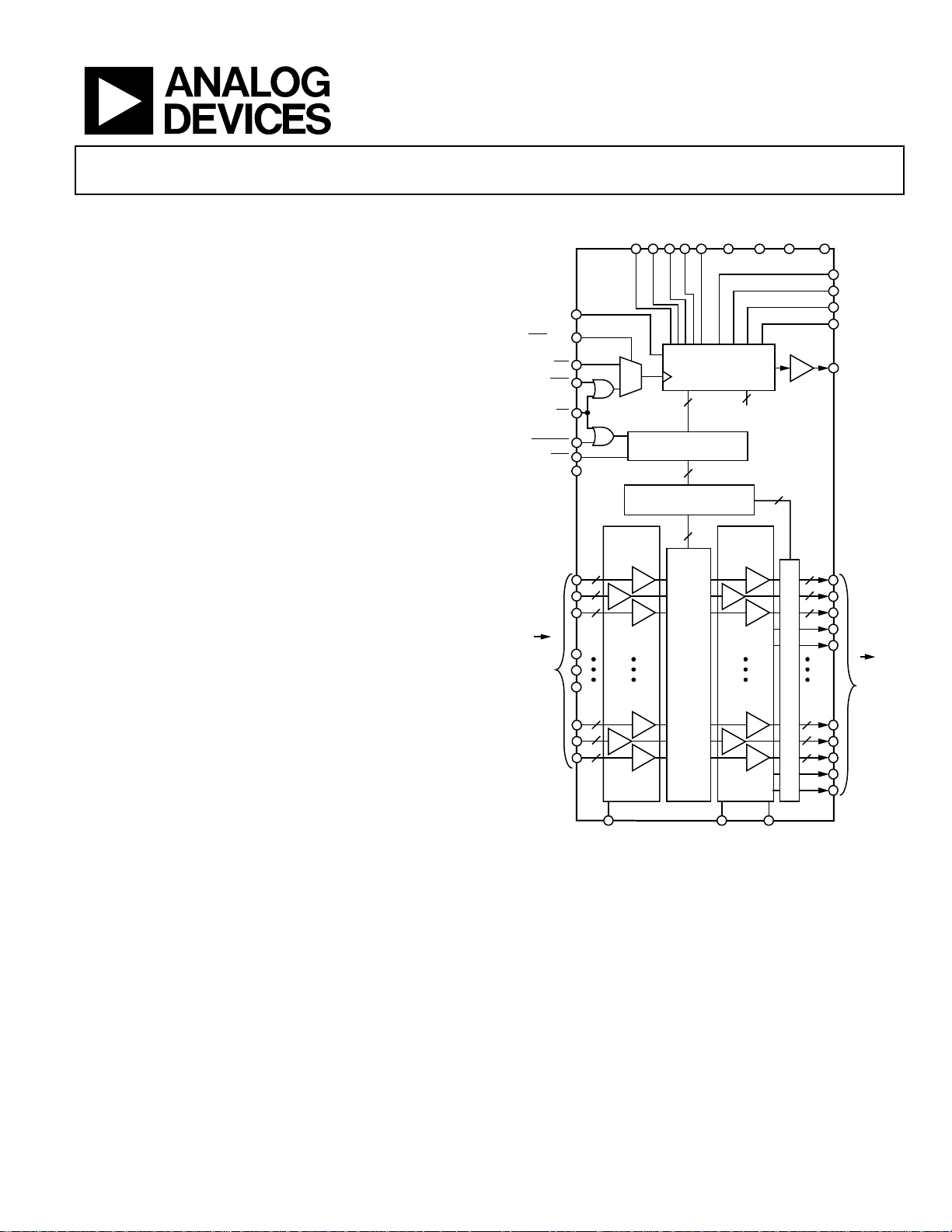
FUNCTIONAL BLOCK DIAGRAM
D0 D1 D2 D3 D4VPOSVNEGVDD DGND
AD8178
SERIN
ER/PAR
WE
CLK
CS
UPDATE
RST
CMENC
R
G
B
16 x RGB
CHANNELS
R
G
B
1
0
INPUT
RECEIVER
G = +2
2
2
2
2
2
2
VBLK VOCM_CMENCON VOCM_CMENCOFF
45-BIT SHIFT
REGISTER WITH
5-BIT PARALLEL
LOADING
25
PARALLEL L ATCH
25
DECODE
5 × 5:16 DECODERS
80
SWITCH
MATRIX
G = +2
20
NO
CONNECT
OUTPUT
BUFFER
G = +1
5
ENABLE/DISABL E
Figure 1.
The outputs can be used single-ended in conjunction with
decoded H and V outputs to drive a monitor directly.
The independent output buffers of the AD8178 can be placed
into a high impedance state to create larger arrays by paralleling
crosspoint outputs. Inputs can be paralleled as well. The AD8178
offers both serial and a parallel programming modes.
The AD8178 is packaged in a fully-populated 26 × 26 ball
PBGA package and is available over the extended industrial
temperature range of −40°C to +85°C.
A0
A1
A2
CLR
SEROUT
SET INDIVIDUAL, OR
RESET ALL OUTPUTS T O OFF
2
2
2
2
2
2
R
G
B
H
V
CHANNELS
5 x RGB, HV
R
G
B
H
V
06608-001
0
Rev.
Information furnished by Analog Devices is believed to be accurate and reliable. However, no
responsibility is assumed by Anal og Devices for its use, nor for any infringements of patents or ot her
rights of third parties that may result from its use. Specifications subject to change without notice. No
license is granted by implication or otherwise under any patent or patent rights of Analog Devices.
Trademarks and registered trademarks are the property of their respective owners.
One Technology Way, P.O. Box 9106, Norwood, MA 02062-9106, U.S.A.
Tel: 781.329.4700 www.analog.com
Fax: 781.461.3113 ©2007 Analog Devices, Inc. All rights reserved.

AD8178
TABLE OF CONTENTS
Features.............................................................................................. 1
Applications....................................................................................... 1
Functional Block Diagram .............................................................. 1
General Description ......................................................................... 1
Revision History ............................................................................... 2
Specifications..................................................................................... 3
Timing Characteristics (Serial Mode) ....................................... 5
Timing Characteristics (Parallel Mode).................................... 6
Absolute Maximum Ratings............................................................ 7
Thermal Resistance ...................................................................... 7
Power Dissipation......................................................................... 7
ESD Caution.................................................................................. 7
REVISION HISTORY
7/07—Revision 0: Initial Version
Pin Configurations and Function Descriptions............................8
Truth Table and Logic Diagram ............................................... 17
Equivalent Circuits......................................................................... 19
Typical Performance Characteristics........................................... 21
Theory of Operation ...................................................................... 26
Applications Information.............................................................. 27
Operating Modes........................................................................ 27
Programming.............................................................................. 28
Differential and Single-Ended Operation............................... 29
Outline Dimensions....................................................................... 38
Ordering Guide .......................................................................... 38
Rev. 0 | Page 2 of 40

AD8178
SPECIFICATIONS
VS = ± 2.5 V at TA = 25°C, G = +4, RL = 100 Ω (each output), VBLK = 0 V, output CM voltage = 0 V, differential I/O mode, unless
otherwise noted.
Table 1.
Parameter Conditions Min Typ Max Unit
DYNAMIC PERFORMANCE
−3 dB Bandwidth 200 mV p-p 450 MHz
2 V p-p 420 MHz
Gain Flatness 0.1 dB, 200 mV p-p 17 MHz
Propagation Delay 2 V p-p 1.3 ns
Settling Time 1% , 2 V step 4 ns
Slew Rate, Differential Output 2 V step 1650 V/μs
2 V step, 10% to 90% 1450 V/μs
Slew Rate, RGB Common Mode 1 V step , 10% to 90% 300 V/μs
Slew Rate, HV Outputs Rail-to-rail, TTL load 400 V/μs
NOISE/DISTORTION PERFORMANCE
Crosstalk, All Hostile f = 5 MHz −82 dB
f = 10 MHz −74 dB
f = 100 MHz −56 dB
f = 500 MHz −47 dB
Off Isolation, Input-Output f = 10 MHz, RL = 100 Ω, one channel −90 dB
Input Voltage Noise 0.01 MHz to 50 MHz 50 nV/√Hz
DC PERFORMANCE
Gain Error 1 %
Gain Matching R, G, B same channel 0.5 %
Gain Temperature Coefficient 32 ppm/°C
OUTPUT CHARACTERISTICS
Output Offset Voltage CMENC on or off 20 mV
Temperature coefficient 58 μV/°C
Output Offset Voltage,
RGB Common Mode
Temperature coefficient −16 μV/°C
Output Impedance Enabled, differential 1.5 Ω
Disabled, differential 2.7 kΩ
Output Disable Capacitance Disabled 2 pF
Output Leakage Current Disabled 1 μA
Output Voltage Range No load, differential 4 V p-p
Output Current Short circuit 45 mA
INPUT CHARACTERISTICS
Input Voltage Range,
Differential Mode
Input Voltage Range,
Common Mode
CMR, RGB Input ΔV
ΔV
CM Gain, RGB Input ΔV
ΔV
Input Capacitance Any switch configuration 2 pF
Input Resistance Differential 3.33 kΩ
Input Offset Current 1 μA
CMENC on or off 10 mV
1 V p-p
V
= 1 V p-p ±2.25 V p-p
IN
/ΔV
, ΔV
OUT, DM
OUT, DM
OUT, CM
OUT, CM
/ΔV
/ΔV
/ΔV
IN, CM
IN, CM
IN, CM
IN, CM
= ±0.5 V, CMENC off –62 dB
IN, CM
, ΔV
= ±0.5 V, CMENC on −45 dB
IN, CM
, ΔV
= ±0.5 V CMENC off −70 dB
IN, CM
, ΔV
= ±0.5 V, CMENC on 0 dB
IN, CM
Rev. 0 | Page 3 of 40

AD8178
Parameter Conditions Min Typ Max Unit
SWITCHING CHARACTERISTICS
Enable On Time
Switching Time, 2 V Step
UPDATE to 50% output
50%
UPDATE to 50% output
50%
POWER SUPPLIES
Supply Current V
, outputs enabled, no load 460 mA
POS
Outputs disabled 290 mA
V
, outputs enabled, no load 460 mA
NEG
Outputs disabled 290 mA
D
, outputs enabled, no load 4 mA
VDD
Supply Voltage Range 4.5 to 5.5 V
PSR ΔV
ΔV
OUT, DM
OUT, DM
/ΔV
/ΔV
POS
NEG
, ΔV
= ±0.5 V −55 dB
POS
, ΔV
= ±0.5 V −55 dB
NEG
OPERATING TEMPERATURE RANGE
Temperature Range Operating (still air) −40 to +85 °C
θJA Operating (still air) 15 °C/W
80 ns
70 ns
Rev. 0 | Page 4 of 40
AD8178
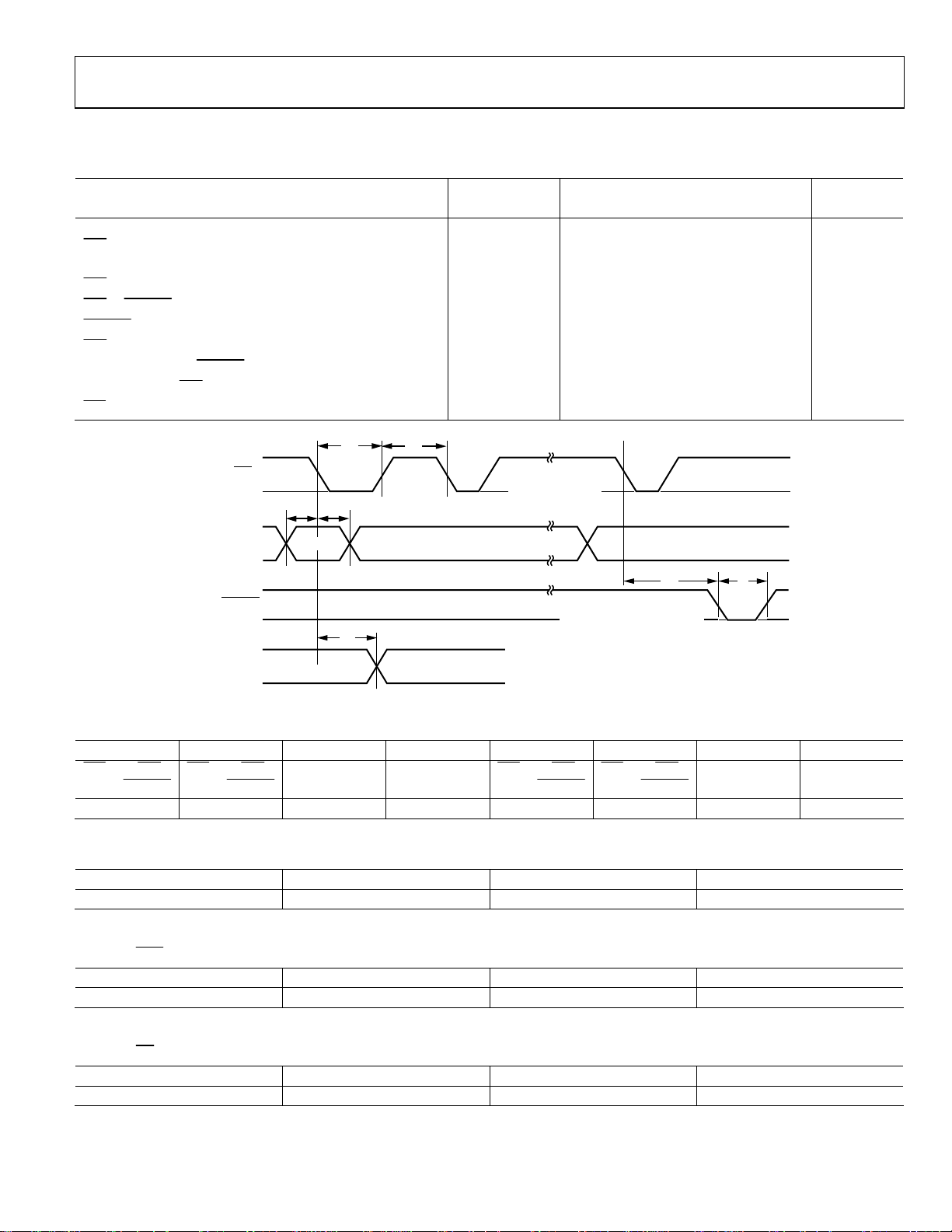
TIMING CHARACTERISTICS (SERIAL MODE)
Table 2.
Limit
Parameter Symbol Min Typ Max Unit
Serial Data Setup Time t1 40 ns
t
CLK Pulse Width
Serial Data Hold Time t3 50 ns
CLK Pulse Separation
CLK to UPDATE Delay
UPDATE Pulse Width
CLK to SEROUT Valid
Propagation Delay, UPDATE to Switch On
Data Load Time, CLK = 5 MHz, Serial Mode
RST Time
60 ns
2
t
140 ns
4
t
10 ns
5
t
90 ns
6
t
120 ns
7
80 ns
9 μs
140 200 ns
CLK
SERIN
1 = LATCHED
UPDATE
0 = TRANSPARENT
SEROUT
t
1
0
t1t
1
OUT4 (D4)
0
1
0
2
3
t
7
t
4
LOAD DATA INTO
SERIAL REGISTER
ON FALLING EDGE
OUT4 (D3) OUT0 (D0)
TRANSFER DATA FROM SERIAL
REGISTER TO PARALLEL
LATCHES DURING LOW LEVEL
t
5
t
6
06608-002
Figure 2. Timing Diagram, Serial Mode
Table 3. Logic Levels, VDD = 3.3 V
VIH VIL V
SER/PAR, CLK,
SERIN, UPDATE
SER/PAR, CLK,
SERIN, UPDATE
V
OH
I
OL
SEROUT SEROUT
I
IH
SER/PAR, CLK,
SERIN, UPDATE
I
IL
SER/PAR, CLK,
SERIN, UPDATE
I
OH
OL
SEROUT SEROUT
2.0 V min 0.6 V max 2.8 V min 0.4 V max 20 μA max –20 μA max –1 mA min 1 mA min
Table 4. H and V Logic Levels, V
VOH VOL I
= 3.3 V
DD
I
OH
OL
2.7 V min 0.5 V max –3 mA max 3 mA max
RST
Table 5.
VIH VIL I
Logic Levels, VDD = 3.3 V
I
IH
IL
2.0 V min 0.6 V max −60 μA max −120 μA max
CS
Table 6.
VOH VOL I
Logic Levels, VDD = 3.3 V
I
IH
OL
2.0 V min 0.6 V max 100 μA max 40 μA max
Rev. 0 | Page 5 of 40
AD8178
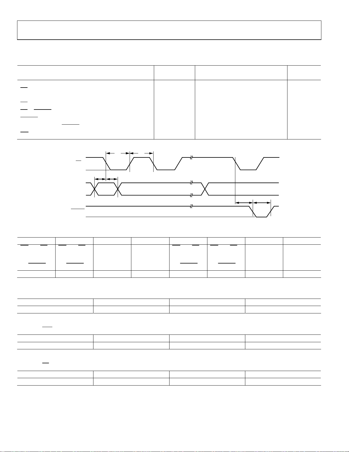
TIMING CHARACTERISTICS (PARALLEL MODE)
Table 7.
Limit
Parameter Symbol Min Typ Max Unit
Parallel Data Setup Time t1 80 ns
t
WE Pulse Width
Parallel Hold Time t3 150 ns
WE Pulse Separation
WE to UPDATE Delay
UPDATE Pulse Width
Propagation Delay, UPDATE to Switch On
RST Time
WE
D0 TO D4
A0 TO A2
1 = LATCHED
0 = TRANSPARENT
UPDATE
t
1
0
t1t
1
0
2
3
t
4
Figure 3. Timing Diagram, Parallel Mode
110 ns
2
t
90 ns
4
t
10 ns
5
t
90 ns
6
80 ns
140 200 ns
t
t
5
6
6608-003
Table 8. Logic Levels, VDD = 3.3 V
VIH VIL V
SER/PAR, WE,
D0, D1, D2, D3,
D4, A0, A1, A2,
A3,
UPDATE
SER/PAR, WE,
D0, D1, D2, D3,
D4, A0, A1, A2,
A3,
UPDATE
V
OH
I
OL
SEROUT SEROUT
I
IH
SER/PAR, WE,
D0, D1, D2, D3,
D4, A0, A1, A2,
A3,
UPDATE
I
IL
SER/PAR, WE,
D0, D1, D2, D3,
D4, A0, A1, A2,
A3,
UPDATE
I
OH
OL
SEROUT SEROUT
2.0 V min 0.6 V max Disabled Disabled 20 μA max −20 μA max Disabled Disabled
Table 9. H and V Logic Levels, V
VOH VOL I
= 3.3 V
DD
I
OH
OL
2.7 V min 0.5 V max –3 mA max 3 mA max
RST
Table 10.
VIH VIL I
Logic Levels, VDD = 3.3 V
I
IH
IL
2.0 V min 0.6 V max −60 μA max −120 μA max
Table 11.
VOH VOL I
CS
Logic Levels, VDD = 3.3 V
I
IH
OL
2.0 V min 0.6 V max 100 μA max 40 μA max
Rev. 0 | Page 6 of 40
AD8178
ABSOLUTE MAXIMUM RATINGS
Table 12.
Parameter Rating
Analog Supply Voltage (V
Digital Supply Voltage (VDD – D
Ground Potential Difference
(V
– D
GND
)
NEG
Maximum Potential Difference
– V
NEG
)
(V
DD
Common-Mode Analog Input Voltage
POS
– V
) 6 V
NEG
) 6 V
GND
+0.5 V to –2.5 V
8 V
– 0.5 V) to
(V
NEG
+ 0.5 V)
(V
POS
Differential Analog Input Voltage ±2 V
Digital Input Voltage VDD
Output Voltage
– 1 V) to (V
POS
NEG
+ 1 V)
(V
(Disabled Analog Output)
Output Short-Circuit Duration Momentary
Storage Temperature Range −65°C to +125°C
Operating Temperature Range −40°C to +85°C
Lead Temperature
300°C
(Soldering, 10 sec)
Junction Temperature 150°C
Stresses above those listed under Absolute Maximum Ratings
may cause permanent damage to the device. This is a stress
rating only; functional operation of the device at these or any
other conditions above those indicated in the operational
section of this specification is not implied. Exposure to absolute
maximum rating conditions for extended periods may affect
device reliability.
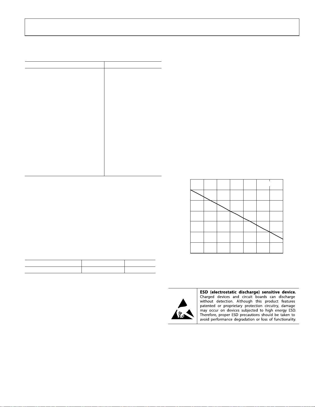
POWER DISSIPATION
The AD8178 is operated with ±2.5 V or +5 V supplies and can
drive loads down to 100 , resulting in a large range of possible
power dissipations. For this reason, extra care must be taken
when derating the operating conditions based on ambient
temperature.
Packaged in a 676-lead BGA, the AD8178 junction-to-ambient
thermal impedance (θ
the maximum allowed junction temperature of the die should
not exceed 150°C. Temporarily exceeding this limit may cause
a shift in parametric performance due to a change in stresses
exerted on the die by the package. Exceeding a junction
temperature of 175°C for an extended period can result in
device failure. The curve in
internal die power dissipations that meet these conditions over
the −40°C to +85°C ambient temperature range. When using
Tabl e 1 3 , do not include external load power in the maximum
power calculation, but do include load current dropped on the
die output transistors.
10
9
8
7
6
) is 15°C/W. For long-term reliability,
JA
Figure 4 shows the range of allowed
TJ = 150°C
THERMAL RESISTANCE
θJA is specified for the worst-case conditions, that is, a device
soldered in a circuit board for surface-mount packages.
Table 13. Thermal Resistance
Package Type θJA Unit
PBGA 15 °C/W
ESD CAUTION
5
MAXIMUM DIE POWER (W)
4
3
15 25 35 45 55 65 75 85
AMBIENT TEM PERATURE (°C)
Figure 4. Maximum Die Power Dissipation vs. Ambient Temperature
6608-004
Rev. 0 | Page 7 of 40
AD8178
PIN CONFIGURATIONS AND FUNCTION DESCRIPTIONS
2625242322212019181716151413121110987654321
VNEG VNEG VNEG NC NC VNEG OPR4 ONB4 VPOS IPR8 INB8 VNEG IPR9 INB9 VPOS IPR10 INB10 VNEG IPR11 INB11 VPOS IPR12 INB12 VNEG VNEG VNEG
A
VNEG VNEG VNEG NC NC VNEG ONR4 OPB4 VPOS INR8 IPB8 VNEG INR9 IPB9 VPOS INR10 IPB10 VNEG INR11 IPB11 VPOS INR12 IPB12 VNEG VNEG VNEG
B
VNEG VNEG VNEG NC NC VNEG OPG4 ONG4 VPOS IPG8 ING8 VNEG IPG9 ING9 VPOS IPG10 ING10 VNEG IPG11 ING11 VPOS IPG12 ING12 VNEG VNEG VNEG
C
VNEG VNEG VNEG NC NC VPOS H4 V4 VPOS VPOS VPOS VPOS VPOS VPOS VPOS VPOS VPOS VPOS VPOS VPOS VPOS VPOS VPOS IPG13 INR13 IPR13
D
VNEG VNEG VNEG VPOS VPOS VPOS VPOS VPOS DGND VDD
E
VPOS VPOS VPOS VPOS VPOS VPOS VPOS VPOS VPOS VPOS VPOS VPOS VPOS VPOS VPOS VPOS VPOS VPOS VPOS VPOS VPOS VPOS VPOS VPOS VPOS VPOS
F
ONB3 OPB3 ONG3 V3 VPOS VPOS VPOS VPOS VPOS VPOS VPOS VPOS VPOS VPOS VPOS VPOS VPOS VPOS VPOS VPOS VPOS VPOS VPOS VPOS VPOS VPOS
G
OPR3 ONR3 OPG3 H3 VPOS VPOS VNEG VNEG VNEG VNEG VNEG VNEG VNEG VNEG VNEG VNEG VNEG VNEG VNEG VPOS VPOS VPOS VPOS IPG14 INR14 IPR14
H
VNEG VNEG VNEG VPOS VPOS VPOS VNEG VNEG VNEG VNEG VNEG VNEG VNEG VNEG VNEG VNEG VNEG VNEG VNEG VPOS VPOS VPOS VPOS ING14 IPB14 INB14
J
NC NC NC NC VPOS VPOS VNEG VNEG VNEG VNEG VNEG VNEG VNEG VNEG VNEG VNEG VNEG VNEG VNEG VPOS VPOS VPOS VPOS VNEG VNEG VNEG
K
NC NC NC NC VPOS VPOS VNEG VNEG VNEG VNEG VNEG VNEG VNEG VNEG VNEG VNEG VNEG VNEG VNEG VPOS VPOS VPOS VPOS IPG15 INR15 IPR15
L
VPOS VPOS VPOS VPOS VPOS VPOS VNEG VNEG VNEG VNEG VNEG VNEG VNEG VNEG VNEG VNEG VNEG VNEG VNEG VPOS VPOS VPOS VPOS ING15 IPB15 INB15
M
ONB2 OPB2 ONG2 V2 VPOS VPOS VNEG VNEG VNEG VNEG VNEG VNEG VNEG VNEG VNEG VNEG VNEG VNEG VNEG VPOS VPOS VPOS VPOS VPOS VPOS
N
OPR2 ONR2 OPG2 H2 VPOS VPOS VNEG VNEG VNEG VNEG VNEG VNEG VNEG VNEG VNEG VNEG VNEG VNEG VNEG VPOS VPOS VBLK VPOS VPOS VPOS VPOS
P
VNEG VNEG VNEG VPOS VPOS VPOS VNEG VNEG VN EG VNEG VNEG VNEG VNEG VNEG VNEG VNEG VNEG VNEG VNEG VPOS VPOS VPOS IPG7 INR7 IPR7
R
NC NC NC NC VPOS VPOS VNEG VNEG VNEG VNEG VNEG VNEG VNEG VNEG VNEG VNEG VNEG VNEG VNEG VPOS VPOS VPOS VPOS ING7 IPB7 INB7
T
NC NC NC NC VPOS VPOS VNEG VNEG VNEG VNEG VNEG VNEG VNEG VNEG VNEG VNEG VNEG VNEG VNEG VPOS VPOS VPOS VPOS VNEG VNEG VNEG
U
VPOS VPOS VPOS VPOS VPOS VPOS VNEG VNEG VNEG VNEG VNEG VNEG VNEG V NEG VNEG VNEG VNEG VNEG VNEG VPOS VPOS VPOS VPOS IPG6 INR6 IPR6
V
ONB1 OPB1 ONG1 V1 VPOS VPOS VNEG VNEG VNEG VNEG VNEG VNEG VNEG VNEG VNEG VNEG VNEG VNEG VNEG VPOS VPOS VPOS VPOS ING6 IPB6 INB6
W
OPR1 ONR1 OPG1 H1 VPOS VPOS VPOS VPOS VPOS VPOS VPOS VPOS VPOS VPOS VPOS VPOS VPOS VPOS VPOS VPOS VPOS VPOS VPOS VPOS VPOS VPOS
Y
VNEG VNEG VNEG VPOS VPOS VPOS VPOS VPOS VPOS VPOS VPOS VPOS VPOS VPOS VPOS VPOS VPOS VPOS VPOS VPOS VPOS VPOS VPOS VPOS VPOS VPOS
AA
VNEG VNEG VNEG VPOS VPOS VPOS VPOS VPOS DGND VDD RST UPDATE WE CMENC D4 D3 D2 D1 D0 VDD DGND VPOS VPOS IPG5 INR5 IPR5
AB
VNEG VNEG VNEG NC NC VPOS V0 H0 VPOS VPOS VPOS VPOS VPOS VPOS VPOS VPOS VPOS VPOS VPOS VPOS VPOS VPOS VPOS ING5 IPB5 INB5
AC
VNEG VNEG VNEG NC NC VPOS ONG0 OPG0 VNEG ING0 IPG0 VPOS ING1 IPG1 VNEG ING2 IPG2 VPOS ING3 IPG3 VNEG ING4 IPG4 VNEG VNEG VNEG
AD
VNEG VNEG VNEG NC NC VPOS OPB0 ONR0 VNEG IPB0 INR0 VPOS IPB1 INR1 VNEG IPB2 INR2 VPOS IPB3 INR3 VNEG IPB4 INR4 VNEG VNEG VNEG
AE
VNEG VNEG VNEG NC NC VPOS ONB0 OPR0 VNEG INB0 IPR0 VPOS INB1 IPR1 VNEG INB2 IPR2 VPOS INB3 IPR3 VNEG INB4 IPR4 VNEG VNEG VNEG
AF
SEROUT
CS CLK SERIN
2625242322212019181716151413121110987654321
Figure 5. Pin Configuration, Package Bottom View
SER/PAR
A2 A1 A0 CLR VDD DGND VPOS VPOS ING13 IPB13 INB13
VOCM_
CMENCON
VOCM_
CMENCOFF
A
B
C
D
E
F
G
H
J
K
L
M
N
P
R
T
U
V
W
Y
AA
AB
AC
AD
AE
AF
06608-055
Rev. 0 | Page 8 of 40
AD8178
1 2 3 4 5 6 7 8 9 101112131415161718192021222324 25 26
A
VNEG VNEG VNEG INB12 IPR12 VPOS INB11 IPR11 VNEG INB10 IPR10 VPOS INB9 IPR9 VNEG INB8 IPR8
B
VNEG VNEG VNEG IPB12 INR12 VPOS IPB11 INR11 VNEG IPB10 INR10 VPOS IPB9 INR9 VNEG IPB8 INR8 VPOS OPB4 ONR4 VNEG NC NC VNEG VNEG VNEG
C
VNEG VNEG VNEG ING12 IPG12 VPOS ING11 IPG11 VNEG ING10 IPG10 VPOS ING9 IPG9 VNEG ING8 IPG8 VPOS ONG4 OPG4 VNEG NC NC VNEG VNEG VNEG
D
IPR13 INR13 IPG13 VPOS VPOS VPOS VPOS VPOS VPOS VPOS VPOS VPOS VPOS VPOS VPOS VPOS VPOS VPOS V4 H4 VPOS NC NC VNEG VNEG VNEG
CS
E
INB13 IPB13 ING13 VPOS VPOS DGND VDD CLR A0 A1 A2
F
VPOS VPOS VPOS VPOS VPOS VPOS VPOS VPOS VPOS VPOS VPOS VPOS VPOS VPOS VPOS VPOS VPOS VPOS VPOS VPOS VPOS VPOS VPOS VPOS VPOS VPOS
G
VPOS VPOS VPOS VPOS VPOS VPOS VPOS VPOS VPOS VPOS VPOS VPOS VPOS VPOS VPOS VPOS VPOS VPOS VPOS VPOS VPOS VPOS V3 ONG3 OPB3 ONB3
H
IPR14 INR14 IPG14 VPOS VPOS VPOS VPOS VNEG VNEG VNEG VNEG VNEG VNEG VNEG VNEG VNEG VNEG VNEG VNEG VNEG VPOS VPOS H3 OPG3
J
INB14 IPB14 ING14 VPOS VPOS VPOS VPOS VNEG VNEG VNEG VNEG VNEG VNEG VNEG VNEG VNEG VNEG VNEG VNEG VNEG VPOS VPOS VPOS VNEG VNEG VNEG
K
VNEG VNEG VNEG VPOS VPOS VPOS VPOS VNEG VNEG VNEG VNEG VNEG VNEG VNEG VNEG VNEG VNEG VNEG VNEG VNEG VPOS VPOS NC NC NC NC
L
IPR15 INR15 IPG15 VPOS VPOS VPOS VPOS VNEG VNEG VNEG VNEG VNEG VNEG VNEG VNEG VNEG VNEG VNEG VNEG VNEG VPOS VPOS NC NC NC NC
M
INB15 IPB15 ING15 VPOS VPOS VPOS VPOS VNEG VNEG VNEG VNEG VNEG VNEG VNEG VNEG VNEG VNEG VNEG VNEG VNEG VPOS VPOS VPOS VPOS VPOS VPOS
N
VPOS VPOS VPOS VPOS
P
VPOS VPOS VPOS VPOS VBLK VPOS VPOS VNEG VNEG VNEG VNEG VNEG VNEG VNEG VNEG VNEG VNEG VNEG VNEG VNEG VPOS VPOS H2 OPG2 ONR2 OPR2
R
IPR7 INR7 IPG7 VPOS
T
INB7 IPB7 ING7 VPOS VPOS VPOS VPOS VNEG VNEG VNEG VNEG VNEG VNEG VNEG VNEG VNEG VNEG VNEG VNEG VNEG VPOS VPOS NC NC NC NC
U
VNEG VNEG VNEG VPOS VPOS VPOS VPOS VNEG VNEG VNEG VNEG VNEG VNEG VNEG VNEG VNEG VNEG VNEG VNEG VNEG VPOS VPOS NC NC NC NC
V
IPR6 INR6 IPG6 VPOS VPOS VPOS VPOS VNEG VNEG VNEG VNEG VNEG VNEG VNEG VNEG VNEG VNEG VNEG VNEG VNEG VPOS VPOS VPOS VPOS VPOS VPOS
W
INB6 IPB6 ING6 VPOS VPOS VPOS VPOS VNEG VNEG VNEG VNEG VNEG VNEG VNEG VNEG VNEG VNEG VNEG VNEG VNEG VPOS VPOS V1 ONG1 OPB1 ONB1
Y
VPOS VPOS VPOS VPOS VPOS VPOS VPOS VPOS VPOS VPOS VPOS VPOS VPOS VPOS VPOS VPOS VPOS VPOS VPOS VPOS VPOS VPOS H1 OPG1 ONR1 OPR1
AA
VPOS VPOS VPOS VPOS VPOS VPOS VPOS VPOS VPOS VPOS VPOS VPOS VPOS VPOS VPOS VPOS VPOS VPOS VPOS VPOS VPOS VPOS VPOS VNEG VNEG VNEG
AB
IPR5 INR5 IPG5 VPOS VPOS DGND VDD D0 D1 D2 D3 D4 CMENC VDD DGND VPOS VPOS VPOS VPOS VPOS VNEG VNEG VNEG
AC
INB5 IPB5 ING5 VPOS VPOS VPOS VPOS VPOS VPOS VPOS VPOS VPOS VPOS VPOS VPOS VPOS VPOS VPOS H0 V0 VPOS NC NC VNEG VNEG VNEG
AD
VNEG V NEG V NEG IPG4 IN G4 V NEG IP G3 IN G3 V POS IP G2 IN G2 VNE G IPG1 IN G1 VP OS IPG0 IN G0 V NEG OP G0 ON G0 VP OS NC NC VN EG VNEG VNEG
AE
VNEG VNEG VNEG INR4 IPB4 VNEG INR3 IPB3 VPOS INR2 IPB2 VNEG INR1 IPB1 VPOS INR0 IPB0 VNEG ONR0 OPB0 VPOS NC NC VNEG VNEG VNEG
AF
VNEG VNEG VNEG IPR4 INB4 VNEG IPR3 INB3 VPOS IPR2 INB2 VNEG IPR1 INB1 VPOS IPR0 INB0 VNEG OPR0 ONB0 VPOS NC NC VNEG VNEG VNEG
VOCM_
VPOS VPOS VNEG VNEG VNEG VNEG VNEG VNEG VNEG VNEG VNEG VNEG VNEG VNEG VNEG VPOS VPOS V2 ONG2 OPB2 ONB2
CMENCON
VOCM_
VPOS VPOS VNEG VNEG VNEG VNEG VNEG VNEG VNEG VNEG VNEG VNEG VNEG VNEG VNEG VPOS VPOS VPOS VNEG VNEG VNEG
CMENCOFF
SER/PAR
SERIN
CLK
UPDATE
SEROUT
RSTWE
1 2 3 4 5 6 7 8 9 101112131415161718192021222324 25 26
Figure 6. Pin Configuration, Package Top View
VPOS ONB4 OPR4 VNEG NC NC VNEG VNEG VNEG
VDD DGND VPOS VPOS VPOS VPOS VPOS VNEG VNEG VNEG
ONR3 OPR3
A
B
C
D
E
F
G
H
J
K
L
M
N
P
R
T
U
V
W
Y
AA
AB
AC
AD
AE
AF
6608-056
Rev. 0 | Page 9 of 40

AD8178
Table 14. Ball Grid Description
Ball No. Mnemonic Description
A1 VNEG Negative Analog Power Supply.
A2 VNEG Negative Analog Power Supply.
A3 VNEG Negative Analog Power Supply.
A4 INB12 Input Number 12, Negative Phase.
A5 IPR12 Input Number 12, Positive Phase.
A6 VPOS Positive Analog Power Supply.
A7 INB11 Input Number 11, Negative Phase.
A8 IPR11 Input Number 11, Positive Phase.
A9 VNEG Negative Analog Power Supply.
A10 INB10 Input Number 10, Negative Phase.
A11 IPR10 Input Number 10, Positive Phase.
A12 VPOS Positive Analog Power Supply.
A13 INB9 Input Number 9, Negative Phase.
A14 IPR9 Input Number 9, Positive Phase.
A15 VNEG Negative Analog Power Supply.
A16 INB8 Input Number 8, Negative Phase.
A17 IPR8 Input Number 8, Positive Phase.
A18 VPOS Positive Analog Power Supply.
A19 ONB4 Output Number 4, Negative Phase.
A20 OPR4 Output Number 4, Positive Phase.
A21 VNEG Negative Analog Power Supply.
A22 NC No Connect.
A23 NC No Connect.
A24 VNEG Negative Analog Power Supply.
A25 VNEG Negative Analog Power Supply.
A26 VNEG Negative Analog Power Supply.
B1 VNEG Negative Analog Power Supply.
B2 VNEG Negative Analog Power Supply.
B3 VNEG Negative Analog Power Supply.
B4 IPB12 Input Number 12, Positive Phase.
B5 INR12 Input Number 12, Negative Phase.
B6 VPOS Positive Analog Power Supply.
B7 IPB11 Input Number 11, Positive Phase.
B8 INR11 Input Number 11, Negative Phase.
B9 VNEG Negative Analog Power Supply.
B10 IPB10 Input Number 10, Positive Phase.
B11 INR10 Input Number 10, Negative Phase.
B12 VPOS Positive Analog Power Supply.
B13 IPB9 Input Number 9, Positive Phase.
B14 INR9 Input Number 9, Negative Phase.
B15 VNEG Negative Analog Power Supply.
B16 IPB8 Input Number 8, Positive Phase.
B17 INR8 Input Number 8, Negative Phase.
B18 VPOS Positive Analog Power Supply.
B19 OPB4 Output Number 4, Positive Phase.
B20 ONR4 Output Number 4, Negative Phase.
B21 VNEG Negative Analog Power Supply.
B22 NC No Connect.
B23 NC No Connect.
B24 VNEG Negative Analog Power Supply.
B25 VNEG Negative Analog Power Supply.
Ball No. Mnemonic Description
B26 VNEG Negative Analog Power Supply.
C1 VNEG Negative Analog Power Supply.
C2 VNEG Negative Analog Power Supply.
C3 VNEG Negative Analog Power Supply.
C4 ING12 Input Number 12, Negative Phase.
C5 IPG12 Input Number 12, Positive Phase.
C6 VPOS Positive Analog Power Supply.
C7 ING11 Input Number 11, Negative Phase.
C8 IPG11 Input Number 11, Positive Phase.
C9 VNEG Negative Analog Power Supply.
C10 ING10 Input Number 10, Negative Phase.
C11 IPG10 Input Number 10, Positive Phase.
C12 VPOS Positive Analog Power Supply.
C13 ING9 Input Number 9, Negative Phase.
C14 IPG9 Input Number 9, Positive Phase.
C15 VNEG Negative Analog Power Supply.
C16 ING8 Input Number 8, Negative Phase.
C17 IPG8 Input Number 8, Positive Phase.
C18 VPOS Positive Analog Power Supply.
C19 ONG4 Output Number 4, Negative Phase.
C20 OPG4 Output Number 4, Positive Phase.
C21 VNEG Negative Analog Power Supply.
C22 NC No Connect.
C23 NC No Connect.
C24 VNEG Negative Analog Power Supply.
C25 VNEG Negative Analog Power Supply.
C26 VNEG Negative Analog Power Supply.
D1 IPR13 Input Number 13, Positive Phase.
D2 INR13 Input Number 13, Negative Phase.
D3 IPG13 Input Number 13, Positive Phase.
D4 VPOS Positive Analog Power Supply.
D5 VPOS Positive Analog Power Supply.
D6 VPOS Positive Analog Power Supply.
D7 VPOS Positive Analog Power Supply.
D8 VPOS Positive Analog Power Supply.
D9 VPOS Positive Analog Power Supply.
D10 VPOS Positive Analog Power Supply.
D11 VPOS Positive Analog Power Supply.
D12 VPOS Positive Analog Power Supply.
D13 VPOS Positive Analog Power Supply.
D14 VPOS Positive Analog Power Supply.
D15 VPOS Positive Analog Power Supply.
D16 VPOS Positive Analog Power Supply.
D17 VPOS Positive Analog Power Supply.
D18 VPOS Positive Analog Power Supply.
D19 V4 Output Number 4, V Sync.
D20 H4 Output Number 4, H Sync.
D21 VPOS Positive Analog Power Supply.
D22 NC No Connect.
D23 NC No Connect.
D24 VNEG Negative Analog Power Supply.
Rev. 0 | Page 10 of 40
AD8178
Ball No. Mnemonic Description
D25 VNEG Negative Analog Power Supply.
D26 VNEG Negative Analog Power Supply.
E1 INB13 Input Number 13, Negative Phase.
E2 IPB13 Input Number 13, Positive Phase.
E3 ING13 Input Number 13, Negative Phase.
E4 VPOS Positive Analog Power Supply.
E5 VPOS Positive Analog Power Supply.
E6 DGND Digital Power Supply.
E7 VDD Digital Power Supply.
E8 CLR Internal Register Clearing
E9 A0 Control Pin 0, Output Address Bit 0.
E10 A1 Control Pin 1, Output Address Bit 1.
E11 A2 Control Pin 2, Output Address Bit 2.
E12
E13 SERIN Control Pin: Serial Data In.
E14
E15
E16 SEROUT Control Pin: Serial Data Out.
E17 VDD Digital Power Supply.
E18 DGND Digital Power Supply.
E19 VPOS Positive Analog Power Supply.
E20 VPOS Positive Analog Power Supply.
E21 VPOS Positive Analog Power Supply.
E22 VPOS Positive Analog Power Supply.
E23 VPOS Positive Analog Power Supply.
E24 VNEG Negative Analog Power Supply.
E25 VNEG Negative Analog Power Supply.
E26 VNEG Negative Analog Power Supply.
F1 VPOS Positive Analog Power Supply.
F2 VPOS Positive Analog Power Supply.
F3 VPOS Positive Analog Power Supply.
F4 VPOS Positive Analog Power Supply.
F5 VPOS Positive Analog Power Supply.
F6 VPOS Positive Analog Power Supply.
F7 VPOS Positive Analog Power Supply.
F8 VPOS Positive Analog Power Supply.
F9 VPOS Positive Analog Power Supply.
F10 VPOS Positive Analog Power Supply.
F11 VPOS Positive Analog Power Supply.
F12 VPOS Positive Analog Power Supply.
F13 VPOS Positive Analog Power Supply.
F14 VPOS Positive Analog Power Supply.
F15 VPOS Positive Analog Power Supply.
F16 VPOS Positive Analog Power Supply.
F17 VPOS Positive Analog Power Supply.
F18 VPOS Positive Analog Power Supply.
F19 VPOS Positive Analog Power Supply.
F20 VPOS Positive Analog Power Supply.
F21 VPOS Positive Analog Power Supply.
F22 VPOS Positive Analog Power Supply.
F23 VPOS Positive Analog Power Supply.
F24 VPOS Positive Analog Power Supply.
SER/PAR
CLK
CS
Control Pin: Serial Parallel Select Mode.
Control Pin: Serial Data Clock.
Control Pin: Chip Select.
Ball No. Mnemonic Description
F25 VPOS Positive Analog Power Supply.
F26 VPOS Positive Analog Power Supply.
G1 VPOS Positive Analog Power Supply.
G2 VPOS Positive Analog Power Supply.
G3 VPOS Positive Analog Power Supply.
G4 VPOS Positive Analog Power Supply.
G5 VPOS Positive Analog Power Supply.
G6 VPOS Positive Analog Power Supply.
G7 VPOS Positive Analog Power Supply.
G8 VPOS Positive Analog Power Supply.
G9 VPOS Positive Analog Power Supply.
G10 VPOS Positive Analog Power Supply.
G11 VPOS Positive Analog Power Supply.
G12 VPOS Positive Analog Power Supply.
G13 VPOS Positive Analog Power Supply.
G14 VPOS Positive Analog Power Supply.
G15 VPOS Positive Analog Power Supply.
G16 VPOS Positive Analog Power Supply.
G17 VPOS Positive Analog Power Supply.
G18 VPOS Positive Analog Power Supply.
G19 VPOS Positive Analog Power Supply.
G20 VPOS Positive Analog Power Supply.
G21 VPOS Positive Analog Power Supply.
G22 VPOS Positive Analog Power Supply.
G23 V3 Output Number 3, V Sync.
G24 ONG3 Output Number 3, Negative Phase.
G25 OPB3 Output Number 3, Positive Phase.
G26 ONB3 Output Number 3, Negative Phase.
H1 IPR14 Input Number 14, Positive Phase.
H2 INR14 Input Number 14, Negative Phase.
H3 IPG14 Input Number 14, Positive Phase.
H4 VPOS Positive Analog Power Supply.
H5 VPOS Positive Analog Power Supply.
H6 VPOS Positive Analog Power Supply.
H7 VPOS Positive Analog Power Supply.
H8 VNEG Negative Analog Power Supply.
H9 VNEG Negative Analog Power Supply.
H10 VNEG Negative Analog Power Supply.
H11 VNEG Negative Analog Power Supply.
H12 VNEG Negative Analog Power Supply.
H13 VNEG Negative Analog Power Supply.
H14 VNEG Negative Analog Power Supply.
H15 VNEG Negative Analog Power Supply.
H16 VNEG Negative Analog Power Supply.
H17 VNEG Negative Analog Power Supply.
H18 VNEG Negative Analog Power Supply.
H19 VNEG Negative Analog Power Supply.
H20 VNEG Negative Analog Power Supply.
H21 VPOS Positive Analog Power Supply.
H22 VPOS Positive Analog Power Supply.
H23 H3 Output Number 3, H Sync.
H24 OPG3 Output Number 3, Positive Phase.
Rev. 0 | Page 11 of 40
AD8178
Ball No. Mnemonic Description
H25 ONR3 Output Number 3, Negative Phase.
H26 OPR3 Output Number 3, Positive Phase.
J1 INB14 Input Number 14, Negative Phase.
J2 IPB14 Input Number 14, Positive Phase.
J3 ING14 Input Number 14, Negative Phase.
J4 VPOS Positive Analog Power Supply.
J5 VPOS Positive Analog Power Supply.
J6 VPOS Positive Analog Power Supply.
J7 VPOS Positive Analog Power Supply.
J8 VNEG Negative Analog Power Supply.
J9 VNEG Negative Analog Power Supply.
J10 VNEG Negative Analog Power Supply.
J11 VNEG Negative Analog Power Supply.
J12 VNEG Negative Analog Power Supply.
J13 VNEG Negative Analog Power Supply.
J14 VNEG Negative Analog Power Supply.
J15 VNEG Negative Analog Power Supply.
J16 VNEG Negative Analog Power Supply.
J17 VNEG Negative Analog Power Supply.
J18 VNEG Negative Analog Power Supply.
J19 VNEG Negative Analog Power Supply.
J20 VNEG Negative Analog Power Supply.
J21 VPOS Positive Analog Power Supply.
J22 VPOS Positive Analog Power Supply.
J23 VPOS Positive Analog Power Supply.
J24 VNEG Negative Analog Power Supply.
J25 VNEG Negative Analog Power Supply.
J26 VNEG Negative Analog Power Supply.
K1 VNEG Negative Analog Power Supply.
K2 VNEG Negative Analog Power Supply.
K3 VNEG Negative Analog Power Supply.
K4 VPOS Positive Analog Power Supply.
K5 VPOS Positive Analog Power Supply.
K6 VPOS Positive Analog Power Supply.
K7 VPOS Positive Analog Power Supply.
K8 VNEG Negative Analog Power Supply.
K9 VNEG Negative Analog Power Supply.
K10 VNEG Negative Analog Power Supply.
K11 VNEG Negative Analog Power Supply.
K12 VNEG Negative Analog Power Supply.
K13 VNEG Negative Analog Power Supply.
K14 VNEG Negative Analog Power Supply.
K15 VNEG Negative Analog Power Supply.
K16 VNEG Negative Analog Power Supply.
K17 VNEG Negative Analog Power Supply.
K18 VNEG Negative Analog Power Supply.
K19 VNEG Negative Analog Power Supply.
K20 VNEG Negative Analog Power Supply.
K21 VPOS Positive Analog Power Supply.
K22 VPOS Positive Analog Power Supply.
K23 NC No Connect.
K24 NC No Connect.
Ball No. Mnemonic Description
K25 NC No Connect.
K26 NC No Connect.
L1 IPR15 Input Number 15, Positive Phase.
L2 INR15 Input Number 15, Negative Phase.
L3 IPG15 Input Number 15, Positive Phase.
L4 VPOS Positive Analog Power Supply.
L5 VPOS Positive Analog Power Supply.
L6 VPOS Positive Analog Power Supply.
L7 VPOS Positive Analog Power Supply.
L8 VNEG Negative Analog Power Supply.
L9 VNEG Negative Analog Power Supply.
L10 VNEG Negative Analog Power Supply.
L11 VNEG Negative Analog Power Supply.
L12 VNEG Negative Analog Power Supply.
L13 VNEG Negative Analog Power Supply.
L14 VNEG Negative Analog Power Supply.
L15 VNEG Negative Analog Power Supply.
L16 VNEG Negative Analog Power Supply.
L17 VNEG Negative Analog Power Supply.
L18 VNEG Negative Analog Power Supply.
L19 VNEG Negative Analog Power Supply.
L20 VNEG Negative Analog Power Supply.
L21 VPOS Positive Analog Power Supply.
L22 VPOS Positive Analog Power Supply.
L23 NC No Connect.
L24 NC No Connect.
L25 NC No Connect.
L26 NC No Connect.
M1 INB15 Input Number 15, Negative Phase.
M2 IPB15 Input Number 15, Positive Phase.
M3 ING15 Input Number 15, Negative Phase.
M4 VPOS Positive Analog Power Supply.
M5 VPOS Positive Analog Power Supply.
M6 VPOS Positive Analog Power Supply.
M7 VPOS Positive Analog Power Supply.
M8 VNEG Negative Analog Power Supply.
M9 VNEG Negative Analog Power Supply.
M10 VNEG Negative Analog Power Supply.
M11 VNEG Negative Analog Power Supply.
M12 VNEG Negative Analog Power Supply.
M13 VNEG Negative Analog Power Supply.
M14 VNEG Negative Analog Power Supply.
M15 VNEG Negative Analog Power Supply.
M16 VNEG Negative Analog Power Supply.
M17 VNEG Negative Analog Power Supply.
M18 VNEG Negative Analog Power Supply.
M19 VNEG Negative Analog Power Supply.
M20 VNEG Negative Analog Power Supply.
M21 VPOS Positive Analog Power Supply.
M22 VPOS Positive Analog Power Supply.
M23 VPOS Positive Analog Power Supply.
M24 VPOS Positive Analog Power Supply.
Rev. 0 | Page 12 of 40

AD8178
Ball No. Mnemonic Description
M25 VPOS Positive Analog Power Supply.
M26 VPOS Positive Analog Power Supply.
N1 VPOS Positive Analog Power Supply.
N2 VPOS Positive Analog Power Supply.
N3 VPOS Positive Analog Power Supply.
N4 VPOS Positive Analog Power Supply.
N5
N6 VPOS Positive Analog Power Supply.
N7 VPOS Positive Analog Power Supply.
N8 VNEG Negative Analog Power Supply.
N9 VNEG Negative Analog Power Supply.
N10 VNEG Negative Analog Power Supply.
N11 VNEG Negative Analog Power Supply.
N12 VNEG Negative Analog Power Supply.
N13 VNEG Negative Analog Power Supply.
N14 VNEG Negative Analog Power Supply.
N15 VNEG Negative Analog Power Supply.
N16 VNEG Negative Analog Power Supply.
N17 VNEG Negative Analog Power Supply.
N18 VNEG Negative Analog Power Supply.
N19 VNEG Negative Analog Power Supply.
N20 VNEG Negative Analog Power Supply.
N21 VPOS Positive Analog Power Supply.
N22 VPOS Positive Analog Power Supply.
N23 V2 Output Number 2, V Sync.
N24 ONG2 Output Number 2, Negative Phase.
N25 OPB2 Output Number 2, Positive Phase.
N26 ONB2 Output Number 2, Negative Phase.
P1 VPOS Positive Analog Power Supply.
P2 VPOS Positive Analog Power Supply.
P3 VPOS Positive Analog Power Supply.
P4 VPOS Positive Analog Power Supply.
P5 VBLK Output Blank Level.
P6 VPOS Positive Analog Power Supply.
P7 VPOS Positive Analog Power Supply.
P8 VNEG Negative Analog Power Supply.
P9 VNEG Negative Analog Power Supply.
P10 VNEG Negative Analog Power Supply.
P11 VNEG Negative Analog Power Supply.
P12 VNEG Negative Analog Power Supply.
P13 VNEG Negative Analog Power Supply.
P14 VNEG Negative Analog Power Supply.
P15 VNEG Negative Analog Power Supply.
P16 VNEG Negative Analog Power Supply.
P17 VNEG Negative Analog Power Supply.
P18 VNEG Negative Analog Power Supply.
P19 VNEG Negative Analog Power Supply.
P20 VNEG Negative Analog Power Supply.
P21 VPOS Positive Analog Power Supply.
P22 VPOS Positive Analog Power Supply.
P23 H2 Output Number 2, H Sync.
P24 OPG2 Output Number 2, Positive Phase.
VOCM_
CMENCON
Output CM Reference with CM
Encoding On.
Ball No. Mnemonic Description
P25 ONR2 Output Number 2, Negative Phase.
P26 OPR2 Output Number 2, Positive Phase.
R1 IPR7 Input Number 7, Positive Phase.
R2 INR7 Input Number 7, Negative Phase.
R3 IPG7 Input Number 7, Positive Phase.
R4 VPOS Positive Analog Power Supply.
R5
R6 VPOS Positive Analog Power Supply.
R7 VPOS Positive Analog Power Supply.
R8 VNEG Negative Analog Power Supply.
R9 VNEG Negative Analog Power Supply.
R10 VNEG Negative Analog Power Supply.
R11 VNEG Negative Analog Power Supply.
R12 VNEG Negative Analog Power Supply.
R13 VNEG Negative Analog Power Supply.
R14 VNEG Negative Analog Power Supply.
R15 VNEG Negative Analog Power Supply.
R16 VNEG Negative Analog Power Supply.
R17 VNEG Negative Analog Power Supply.
R18 VNEG Negative Analog Power Supply.
R19 VNEG Negative Analog Power Supply.
R20 VNEG Negative Analog Power Supply.
R21 VPOS Positive Analog Power Supply.
R22 VPOS Positive Analog Power Supply.
R23 VPOS Positive Analog Power Supply.
R24 VNEG Negative Analog Power Supply.
R25 VNEG Negative Analog Power Supply.
R26 VNEG Negative Analog Power Supply.
T1 INB7 Input Number 7, Negative Phase.
T2 IPB7 Input Number 7, Positive Phase.
T3 ING7 Input Number 7, Negative Phase.
T4 VPOS Positive Analog Power Supply.
T5 VPOS Positive Analog Power Supply.
T6 VPOS Positive Analog Power Supply.
T7 VPOS Positive Analog Power Supply.
T8 VNEG Negative Analog Power Supply.
T9 VNEG Negative Analog Power Supply.
T10 VNEG Negative Analog Power Supply.
T11 VNEG Negative Analog Power Supply.
T12 VNEG Negative Analog Power Supply.
T13 VNEG Negative Analog Power Supply.
T14 VNEG Negative Analog Power Supply.
T15 VNEG Negative Analog Power Supply.
T16 VNEG Negative Analog Power Supply.
T17 VNEG Negative Analog Power Supply.
T18 VNEG Negative Analog Power Supply.
T19 VNEG Negative Analog Power Supply.
T20 VNEG Negative Analog Power Supply.
T21 VPOS Positive Analog Power Supply.
T22 VPOS Positive Analog Power Supply.
T23 NC No Connect.
T24 NC No Connect.
VOCM_
CMENCOFF
Output Reference with CM
Encoding Off.
Rev. 0 | Page 13 of 40

AD8178
Ball No. Mnemonic Description
T25 NC No Connect.
T26 NC No Connect.
U1 VNEG Negative Analog Power Supply.
U2 VNEG Negative Analog Power Supply.
U3 VNEG Negative Analog Power Supply.
U4 VPOS Positive Analog Power Supply.
U5 VPOS Positive Analog Power Supply.
U6 VPOS Positive Analog Power Supply.
U7 VPOS Positive Analog Power Supply.
U8 VNEG Negative Analog Power Supply.
U9 VNEG Negative Analog Power Supply.
U10 VNEG Negative Analog Power Supply.
U11 VNEG Negative Analog Power Supply.
U12 VNEG Negative Analog Power Supply.
U13 VNEG Negative Analog Power Supply.
U14 VNEG Negative Analog Power Supply.
U15 VNEG Negative Analog Power Supply.
U16 VNEG Negative Analog Power Supply.
U17 VNEG Negative Analog Power Supply.
U18 VNEG Negative Analog Power Supply.
U19 VNEG Negative Analog Power Supply.
U20 VNEG Negative Analog Power Supply.
U21 VPOS Positive Analog Power Supply.
U22 VPOS Positive Analog Power Supply.
U23 NC No Connect.
U24 NC No Connect.
U25 NC No Connect.
U26 NC No Connect.
V1 IPR6 Input Number 6, Positive Phase.
V2 INR6 Input Number 6, Negative Phase.
V3 IPG6 Input Number 6, Positive Phase.
V4 VPOS Positive Analog Power Supply.
V5 VPOS Positive Analog Power Supply.
V6 VPOS Positive Analog Power Supply.
V7 VPOS Positive Analog Power Supply.
V8 VNEG Negative Analog Power Supply.
V9 VNEG Negative Analog Power Supply.
V10 VNEG Negative Analog Power Supply.
V11 VNEG Negative Analog Power Supply.
V12 VNEG Negative Analog Power Supply.
V13 VNEG Negative Analog Power Supply.
V14 VNEG Negative Analog Power Supply.
V15 VNEG Negative Analog Power Supply.
V16 VNEG Negative Analog Power Supply.
V17 VNEG Negative Analog Power Supply.
V18 VNEG Negative Analog Power Supply.
V19 VNEG Negative Analog Power Supply.
V20 VNEG Negative Analog Power Supply.
V21 VPOS Positive Analog Power Supply.
V22 VPOS Positive Analog Power Supply.
V23 VPOS Positive Analog Power Supply.
V24 VPOS Positive Analog Power Supply.
Ball No. Mnemonic Description
V25 VPOS Positive Analog Power Supply.
V26 VPOS Positive Analog Power Supply.
W1 INB6 Input Number 6, Negative Phase.
W2 IPB6 Input Number 6, Positive Phase.
W3 ING6 Input Number 6, Negative Phase.
W4 VPOS Positive Analog Power Supply.
W5 VPOS Positive Analog Power Supply.
W6 VPOS Positive Analog Power Supply.
W7 VPOS Positive Analog Power Supply.
W8 VNEG Negative Analog Power Supply.
W9 VNEG Negative Analog Power Supply.
W10 VNEG Negative Analog Power Supply.
W11 VNEG Negative Analog Power Supply.
W12 VNEG Negative Analog Power Supply.
W13 VNEG Negative Analog Power Supply.
W14 VNEG Negative Analog Power Supply.
W15 VNEG Negative Analog Power Supply.
W16 VNEG Negative Analog Power Supply.
W17 VNEG Negative Analog Power Supply.
W18 VNEG Negative Analog Power Supply.
W19 VNEG Negative Analog Power Supply.
W20 VNEG Negative Analog Power Supply.
W21 VPOS Positive Analog Power Supply.
W22 VPOS Positive Analog Power Supply.
W23 V1 Output Number 1, V Sync.
W24 ONG1 Output Number 1, Negative Phase.
W25 OPB1 Output Number 1, Positive Phase.
W26 ONB1 Output Number 1, Negative Phase.
Y1 VPOS Positive Analog Power Supply.
Y2 VPOS Positive Analog Power Supply.
Y3 VPOS Positive Analog Power Supply.
Y4 VPOS Positive Analog Power Supply.
Y5 VPOS Positive Analog Power Supply.
Y6 VPOS Positive Analog Power Supply.
Y7 VPOS Positive Analog Power Supply.
Y8 VPOS Positive Analog Power Supply.
Y9 VPOS Positive Analog Power Supply.
Y10 VPOS Positive Analog Power Supply.
Y11 VPOS Positive Analog Power Supply.
Y12 VPOS Positive Analog Power Supply.
Y13 VPOS Positive Analog Power Supply.
Y14 VPOS Positive Analog Power Supply.
Y15 VPOS Positive Analog Power Supply.
Y16 VPOS Positive Analog Power Supply.
Y17 VPOS Positive Analog Power Supply.
Y18 VPOS Positive Analog Power Supply.
Y19 VPOS Positive Analog Power Supply.
Y20 VPOS Positive Analog Power Supply.
Y21 VPOS Positive Analog Power Supply.
Y22 VPOS Positive Analog Power Supply.
Y23 H1 Output Number 1, H Sync.
Y24 OPG1 Output Number 1, Positive Phase.
Rev. 0 | Page 14 of 40

AD8178
Ball No. Mnemonic Description
Y25 ONR1 Output Number 1, Negative Phase.
Y26 OPR1 Output Number 1, Positive Phase.
AA1 VPOS Positive Analog Power Supply.
AA2 VPOS Positive Analog Power Supply.
AA3 VPOS Positive Analog Power Supply.
AA4 VPOS Positive Analog Power Supply.
AA5 VPOS Positive Analog Power Supply.
AA6 VPOS Positive Analog Power Supply.
AA7 VPOS Positive Analog Power Supply.
AA8 VPOS Positive Analog Power Supply.
AA9 VPOS Positive Analog Power Supply.
AA10 VPOS Positive Analog Power Supply.
AA11 VPOS Positive Analog Power Supply.
AA12 VPOS Positive Analog Power Supply.
AA13 VPOS Positive Analog Power Supply.
AA14 VPOS Positive Analog Power Supply.
AA15 VPOS Positive Analog Power Supply.
AA16 VPOS Positive Analog Power Supply.
AA17 VPOS Positive Analog Power Supply.
AA18 VPOS Positive Analog Power Supply.
AA19 VPOS Positive Analog Power Supply.
AA20 VPOS Positive Analog Power Supply.
AA21 VPOS Positive Analog Power Supply.
AA22 VPOS Positive Analog Power Supply.
AA23 VPOS Positive Analog Power Supply.
AA24 VNEG Negative Analog Power Supply.
AA25 VNEG Negative Analog Power Supply.
AA26 VNEG Negative Analog Power Supply.
AB1 IPR5 Input Number 5, Positive Phase.
AB2 INR5 Input Number 5, Negative Phase.
AB3 IPG5 Input Number 5, Positive Phase.
AB4 VPOS Positive Analog Power Supply.
AB5 VPOS Positive Analog Power Supply.
AB6 DGND Digital Power Supply.
AB7 VDD Digital Power Supply.
AB8 D0 Control Pin, Input Address Bit 0.
AB9 D1 Control Pin, Input Address Bit 1.
AB10 D2 Control Pin, Input Address Bit 2.
AB11 D3 Control Pin, Input Address Bit 3.
AB12 D4 Control Pin, Input Address Bit 4.
AB13 CMENC Control Pin, Pass/Stop CM Encoding.
AB14
AB15
AB16
AB17 VDD Digital Power Supply.
AB18 DGND Digital Power Supply.
AB19 VPOS Positive Analog Power Supply.
AB20 VPOS Positive Analog Power Supply.
AB21 VPOS Positive Analog Power Supply.
AB22 VPOS Positive Analog Power Supply.
AB23 VPOS Positive Analog Power Supply.
AB24 VNEG Negative Analog Power Supply.
WE
UPDATE
RST
Control Pin, 1st Rank Write Strobe.
Control Pin, 2nd Rank Write Strobe.
Control Pin, 2nd Rank Data Reset.
Ball No. Mnemonic Description
AB25 VNEG Negative Analog Power Supply.
AB26 VNEG Negative Analog Power Supply.
AC1 INB5 Input Number 5, Negative Phase.
AC2 IPB5 Input Number 5, Positive Phase.
AC3 ING5 Input Number 5, Negative Phase.
AC4 VPOS Positive Analog Power Supply.
AC5 VPOS Positive Analog Power Supply.
AC6 VPOS Positive Analog Power Supply.
AC7 VPOS Positive Analog Power Supply.
AC8 VPOS Positive Analog Power Supply.
AC9 VPOS Positive Analog Power Supply.
AC10 VPOS Positive Analog Power Supply.
AC11 VPOS Positive Analog Power Supply.
AC12 VPOS Positive Analog Power Supply.
AC13 VPOS Positive Analog Power Supply.
AC14 VPOS Positive Analog Power Supply.
AC15 VPOS Positive Analog Power Supply.
AC16 VPOS Positive Analog Power Supply.
AC17 VPOS Positive Analog Power Supply.
AC18 VPOS Positive Analog Power Supply.
AC19 H0 Output Number 0, H Sync.
AC20 V0 Output Number 0, V Sync.
AC21 VPOS Positive Analog Power Supply.
AC22 NC No Connect.
AC23 NC No Connect.
AC24 VNEG Negative Analog Power Supply.
AC25 VNEG Negative Analog Power Supply.
AC26 VNEG Negative Analog Power Supply.
AD1 VNEG Negative Analog Power Supply.
AD2 VNEG Negative Analog Power Supply.
AD3 VNEG Negative Analog Power Supply.
AD4 IPG4 Input Number 4, Positive Phase.
AD5 ING4 Input Number 4, Negative Phase.
AD6 VNEG Negative Analog Power Supply.
AD7 IPG3 Input Number 3, Positive Phase.
AD8 ING3 Input Number 3, Negative Phase.
AD9 VPOS Positive Analog Power Supply.
AD10 IPG2 Input Number 2, Positive Phase.
AD11 ING2 Input Number 2, Negative Phase.
AD12 VNEG Negative Analog Power Supply.
AD13 IPG1 Input Number 1, Positive Phase.
AD14 ING1 Input Number 1, Negative Phase.
AD15 VPOS Positive Analog Power Supply.
AD16 IPG0 Input Number 0, Positive Phase.
AD17 ING0 Input Number 0, Negative Phase.
AD18 VNEG Negative Analog Power Supply.
AD19 OPG0 Output Number 0, Positive Phase.
AD20 ONG0 Output Number 0, Negative Phase.
AD21 VPOS Positive Analog Power Supply.
AD22 NC No Connect.
AD23 NC No Connect.
AD24 VNEG Negative Analog Power Supply.
Rev. 0 | Page 15 of 40

AD8178
Ball No. Mnemonic Description
AD25 VNEG Negative Analog Power Supply.
AD26 VNEG Negative Analog Power Supply.
AE1 VNEG Negative Analog Power Supply.
AE2 VNEG Negative Analog Power Supply.
AE3 VNEG Negative Analog Power Supply.
AE4 INR4 Input Number 4, Negative Phase.
AE5 IPB4 Input Number 4, Positive Phase.
AE6 VNEG Negative Analog Power Supply.
AE7 INR3 Input Number 3, Negative Phase.
AE8 IPB3 Input Number 3, Positive Phase.
AE9 VPOS Positive Analog Power Supply.
AE10 INR2 Input Number 2, Negative Phase.
AE11 IPB2 Input Number 2, Positive Phase.
AE12 VNEG Negative Analog Power Supply.
AE13 INR1 Input Number 1, Negative Phase.
AE14 IPB1 Input Number 1, Positive Phase.
AE15 VPOS Positive Analog Power Supply.
AE16 INR0 Input Number 0, Negative Phase.
AE17 IPB0 Input Number 0, Positive Phase.
AE18 VNEG Negative Analog Power Supply.
AE19 ONR0 Output Number 0, Negative Phase.
AE20 OPB0 Output Number 0, Positive Phase.
AE21 VPOS Positive Analog Power Supply.
AE22 NC No Connect.
AE23 NC No Connect.
AE24 VNEG Negative Analog Power Supply.
AE25 VNEG Negative Analog Power Supply.
Ball No. Mnemonic Description
AE26 VNEG Negative Analog Power Supply.
AF1 VNEG Negative Analog Power Supply.
AF2 VNEG Negative Analog Power Supply.
AF3 VNEG Negative Analog Power Supply.
AF4 IPR4 Input Number 4, Positive Phase.
AF5 INB4 Input Number 4, Negative Phase.
AF6 VNEG Negative Analog Power Supply.
AF7 IPR3 Input Number 3, Positive Phase.
AF8 INB3 Input Number 3, Negative Phase.
AF9 VPOS Positive Analog Power Supply.
AF10 IPR2 Input Number 2, Positive Phase.
AF11 INB2 Input Number 2, Negative Phase.
AF12 VNEG Negative Analog Power Supply.
AF13 IPR1 Input Number 1, Positive Phase.
AF14 INB1 Input Number 1, Negative Phase.
AF15 VPOS Positive Analog Power Supply.
AF16 IPR0 Input Number 0, Positive Phase.
AF17 INB0 Input Number 0, Negative Phase.
AF18 VNEG Negative Analog Power Supply.
AF19 OPR0 Output Number 0, Positive Phase.
AF20 ONB0 Output Number 0, Negative Phase.
AF21 VPOS Positive Analog Power Supply.
AF22 NC No Connect.
AF23 NC No Connect.
AF24 VNEG Negative Analog Power Supply.
AF25 VNEG Negative Analog Power Supply.
AF26 VNEG Negative Analog Power Supply.
Rev. 0 | Page 16 of 40

AD8178
TRUTH TABLE AND LOGIC DIAGRAM
Table 15. Operation Truth Table
/PAR
WE UPDATE CLK
1
X
X X X X 0 X X X
1 1
SERIN SEROUT
SERIN
SERIN
i
RST
1 0 0 X
i-45
0 1 1 X X 1 1 0 X
1 0 1 X X 1 X 0 X
1 X X X X 1 1 0 X No change in logic.
1
X = don’t care.
SER
CS
CMENC Operation/Comment
Asynchronous reset. All outputs
are disabled. Contents of the
45-bit shift register are
unchanged.
Serial mode. The data on the
SERIN line is loaded into the
45-bit shift register. The first bit
clocked into the shift register
appears at SEROUT 45 clock
cycles later. Data is not applied
to the switch array.
Parallel mode. The data on
parallel lines D0 through D4 is
loaded into the shift register
location addressed by A0
through A2. Data is not applied
to the switch array.
Switch array update. Data in
the 45-bit shift register is transferred to the parallel latches
and applied to the switch array.
Rev. 0 | Page 17 of 40

AD8178
SEROUT
DQ
CLK
Q
S
D1
D0
DQ
CLK
Q
S
D1
D0
DQ
CLK
Q
S
D1
D0
DQ
CLK
Q
S
D1
D0
DQ
CLK
Q
S
D1
D0
CLK
Q
S
D1
D0
CLK
DQ
Q
S
D1
D0
D
ENA
D
ENA
D
ENA
D
ENA
D
ENA
D
ENA
D
ENA
Q
EN
OUT4
CLR
Q
B3
OUT4
CLR
Q
B2
OUT4
CLR
Q
B1
OUT4
CLR
Q
B0
OUT4
CLR
Q
EN
OUT4
CLR
Q
B0
OUT1
CLR
06608-028
5
OUTPUT ENABLE
DECODE
D0D1D2D3D4
D
Q
EN
DQ DQ
CLK
Q
S
D1
D0
DQ
CLK
Q
S
D1
D0
DQ
CLK
Q
S
D1
D0
DQ
CLK
Q
S
D1
D0
DQ
CLK
Q
S
D1
D0
ENA
D
ENA
D
ENA
D
ENA
D
ENA
OUT0
CLR
Q
B3
OUT0
CLR
Q
B2
OUT0
CLR
Q
B1
OUT0
CLR
Q
B0
OUT0
CLR
UPDATE
80
SWITCH MATRIX
CS
RST
OUT0 EN
CS
WE
SER/PAR
PARALLEL DATA
(OUTPUT ENABLE)
SERIN
CLK
OUT1 EN
OUT2 EN
3 TO 5 DECODER
ADDRESS
OUTPUT
A2A1A0
OUT3 EN
OUT4 EN
Figure 7. Logic Diagram
Rev. 0 | Page 18 of 40

AD8178
V
n
Ω
Ω
n
n
V
V
V
V
V
V
EQUIVALENT CIRCUITS
POS
OPn, ONn
1kΩ
1kΩ
(VPOS – VNEG)
2
Figure 8. Enabled Output (see also ESD Protection Map,
3.4pF
0.4pF 3.1kΩ
3.4pF
Figure 9. Disabled Output (see also ESD Protection Map,
IPn
IN
1.3pF
0.3pF
1.3pF
2500
10kΩ
2500Ω 5050Ω
POS
VNEG
VPOS
VNEG
5050
20kΩ
20kΩ
20kΩ
20kΩ
06608-008
Figure 19)
Figure 19)
Figure 10. Receiver Differential (see also ESD Protection Map,
OPn
ONn
06608-009
06608-010
Figure 19)
VNEG
10kΩ
06608-013
BLK,
OCM_CMENCOFF
0.1pF
0.1pF 10kΩ
Figure 13. VBLK and VOCM_CMENCOFF Inputs
POS
VNEG
Figure 19)
3.33kΩ
06608-014
(see also ESD Protection Map,
0.3pF
OCM_CMENCON
0.3pF 3.33kΩ
Figure 14. VOCM_CMENCON Input (see also ESD Protection Map, Figure 19)
DD
25kΩ
1kΩ
DGND
06608-015
Figure 15.
RST
RST
Input (see also ESD Protection Map, Figure 19)
IP
INn
Figure 11. Receiver Simplified Equivalent Circuit When Driving Differentially
Figure 12. Receiver Simplified Equivalent Circuit When Driving Single-Ended
0.3pF
IP
INn
1.3pF
1.3pF
1.6pF
10kΩ
2.5kΩ
2500Ω
2500Ω
06608-012
CLK, SER/PAR, WE,
UPDATE, SERIN
A[2:0], D[4:0] ,
06608-011
CMENC
Figure 16. Logic Input (see also ESD Protection Map,
CS
25kΩ
CS
Figure 17.
Input (see also ESD Protection Map, Figure 19)
1kΩ
1kΩ
DGND
DGND
06608-030
06608-016
Figure 19)
Rev. 0 | Page 19 of 40

AD8178
V
V
V
DD
SEROUT,
H, V
DGND
06608-017
Figure 18.SEROUT, H, V Logic Outputs
(see also ESD Protection Map,
Figure 19)
IPn, INn,
OPn, ONn, VBLK,
VOCM_CM ENCOF F
VOCM_CM ENCON
POS
VNEG DGND
DD
Figure 19. ESD Protection Map
CLK, RST,
SER/PAR,
WE,
UPDATE,
SERIN,
SEROUT,
A[2:0],
D[4:0],
CMENC,
CS
06608-018
Rev. 0 | Page 20 of 40

AD8178
TYPICAL PERFORMANCE CHARACTERISTICS
VS = ±2.5 V at TA = 25°C, G = +2, RL = 100 Ω (each output), VBLK = 0 V, output CM voltage = 0 V, differential I/O mode, unless
otherwise noted.
20
18
16
14
12
10
GAIN (dB)
8
6
4
2
0
1 10 100 1000
FREQUENCY (MHz)
Figure 20. Small Signal Frequency Response, 200 mV p-p
06608-019
0.15
0.10
0.05
0
, DIFF (V)
OUT
V
–0.05
–0.10
–0.15
0 2 4 6 8 101214161820
TIME (ns)
Figure 23. Small Signal Pulse Response, 200 mV p-p
6608-032
18
16
14
12
10
8
GAIN (dB)
6
4
2
0
–2
1 10 100 1000
FREQUENCY (MHz)
Figure 21. Large Signal Frequency Response, 2 V p-p
22
20
18
16
14
12
10
GAIN (dB)
8
6
4
2
0
1 10 100 1000
FREQUENCY (MHz)
10pF
5pF
2pF
0pF
Figure 22. Small Signal Frequency Response with Capacitive Loads
1.5
1.0
0.5
0
, DIFF (V)
OUT
V
–0.5
–1.0
–1.5
0 2 4 6 8 101214161820
6608-020
TIME (ns)
06608-033
Figure 24. Large Signal Pulse Response, 2 V p-p
15
V
OUT
10
V
IN
5
0
–5
–10
OUTPUT ERROR (%)
–15
–20
–25
012345678
06608-031
TIME (ns)
ERROR
1.2
0.9
0.6
0.3
0
–0.3
–0.6
–0.9
–1.2
, DIFF (V)
OUT
V
06608-034
Figure 25. Settling Time
Rev. 0 | Page 21 of 40

AD8178
5
4
3
2
1
0
–1
OUTPUT ERROR (%)
–2
–3
–4
–5
012345678
TIME (ns)
Figure 26. Settling Time, 1% Zoom
2
1
0
–1
, DIFF (V)
–2
OUT
V
–3
1650V/µs PEAK
6000
5000
4000
3000
2000
1000
6608-035
SLEW RATE (V/µs)
0
–10
–20
–30
–40
–50
–60
CROSSTALK (d B)
–70
–80
–90
–100
1 10 100 1000
FREQUENCY (MHz )
Figure 29. Crosstalk, All Hostile
0
–20
–40
–60
–80
FEEDTHROUG H (dB)
6608-038
–4
–5
012345678910
TIME (ns)
Figure 27. Large Signal Rising Edge Slew Rate
0
–10
–20
–30
–40
–50
CROSSTALK (d B)
–60
–70
–80
1 10 100 1000
FREQUENCY (MHz )
Figure 28. Crosstalk, All Hostile, Single-Ended
0
–1000
–100
–120
1 10 100 1000
06608-036
FREQUENCY (MHz)
06608-039
Figure 30. Crosstalk, Off Isolation
0
–10
–20
–30
–40
CMR (dB)
–50
–60
–70
1 10 100 1000
06608-037
CMENC HIGH
CMENC LOW
FREQUENCY (MHz )
06608-040
Figure 31. Common-Mode Rejection
Rev. 0 | Page 22 of 40

AD8178
600
|I
| AND |I
500
400
| (mA)
NEG
300
| AND |I
200
POS
|I
100
0
–50–40–30–20–100 102030405060708090100
POS
(BROADCAST)
|I
| AND |I
POS
(ALL OUTPUTS DISABLE D)
|
NEG
|
NEG
TEMPERATURE ( °C)
Figure 32. Quiescent Supply Currents vs. Temperature
3000
2500
2000
1500
6608-041
10000
1000
IMPEDANCE (Ω)
100
1 10 100 1000
FREQUENCY (MHz)
Figure 35. Input Impedance
10000
1000
6608-044
IMPEDANCE (Ω)
1000
500
0
1 10 100 1000
FREQUENCY (MHz)
Figure 33. Output Impedance, Disabled
100
90
80
70
60
50
40
IMPEDANCE (Ω)
30
20
10
0
1 10 100 1000
FREQUENCY (MHz)
Figure 34. Output Impedance, Enabled
IMPEDANCE (Ω)
100
1 10 100 1000
06608-042
FREQUENCY (MHz )
06608-045
Figure 36. Input Impedance, Single-Ended
0
–10
–20
–30
–40
–50
BALANCE ERROR (dB)
–60
–70
–80
1 10 100 1000
06608-043
FREQUENCY (MHz )
06608-046
Figure 37. Output Balance Error
Rev. 0 | Page 23 of 40

AD8178
1.0
20
1400
0.5
0
–0.5
, COMM ON MO DE (V)
OUT
V
–1.0
–1.5
0 100 200 300 400 500 600 700 800 900 1000
BLUE
HSYNC
TIME (ns)
RED
Figure 38. Common-Mode Pulse Response
0
–10
–20
–30
–40
–50
FEEDTHROUG H (dB)
–60
–70
–80
1 10 100 1000
FREQUENCY (MHz )
Figure 39. Common-Mode Isolation, CMENC Low
GREEN
VSYNC
15
10
(V)
OUT
V
5
0
–5
6608-047
06608-048
1200
1000
800
COUNT
600
400
200
0
–70 –60 –50 –40 –30 –20 –10 0 10 20 30 40 50 60 70
VOS (mV)
Figure 41. V
5
4
3
2
1
0
(mV)
OS
V
–1
–2
–3
–4
–5
–40 –20 0 20 40 60 80 100
Figure 42. V
Distribution
OS
58µV/°C
TEMPERATURE ( °C)
Drift, RTO
OS
06608-050
06608-051
200
160
120
80
40
NOISE SPECTRAL DENSITY (nV/√Hz)
0
0 102030405060708090100
FREQUENCY (MHz )
Figure 40. Noise Spectral Density
6608-049
Rev. 0 | Page 24 of 40
1.5
1.0
0.5
0
–0.5
COMMON MODE (mV)
OS
V
–1.0
–1.5
–40–200 20406080100
Figure 43. V
–16µV/°C
TEMPERATURE ( °C)
Drift, Common Mode, RTO
OS
06608-052

AD8178
5
4
UPDATE
3
2
UPDATE (V)
1
0
–1
0 20 40 60 80 100 120 140 160 180 200 220 240 260 280
TIME (ns)
Figure 44. Enable Time
1.25
1.00
V
OUT
0.75
0.50
, SINGLE-ENDED (V)
0.25
OUT
V
0
–0.25
06608-053
0.020
0.015
0.010
0.005
0
–0.005
–0.010
NORMALIZE D DC GAIN (dB)
–0.015
–0.020
–40 –20 0 20 40 60 80 100
TEMPERATURE (° C)
32ppm/°C
06608-054
Figure 45. Normalized DC Gain vs. Temperature
Rev. 0 | Page 25 of 40

AD8178
THEORY OF OPERATION
The AD8178 is a nonblocking crosspoint with 16 RGB input
channels and 5 RGB output channels. Architecturally, the
AD8178 is a differential-in, differential-out crosspoint suited
for middle-of-Cat-5-run applications. Furthermore, its
differential-in, differential-out gain of +4 and its decoded H and
V sync outputs make it the ideal solution for driving a monitor
directly. The ability to set the output common-mode (CM) and
black level through external pins offers additional flexibility.
Processing of CM voltage levels is achieved by placing the AD8178
in either of its two operation modes. In the first operation mode
(CMENC low), the input CM of each RGB differential pair
(possibly present in the form of either sync-on CM signaling or
noise) is removed through the switch, and the output CM is set
to a global reference voltage via the VOCM_CMENCOFF analog
input. In this mode, the AD8178 behaves as a traditional
differential-in, differential-out switch. If sync-on CM signaling
is present at the differential RGB inputs, then the H and V
outputs represent decoded syncs. In the second operation mode
(CMENC high), input sync-on CM signaling is propagated
through the switch with unity gain. In this mode, the overall
output CM is set to a global reference voltage via the
VOCM_CMENCON analog input. Note that in both operation
modes, the overall input CM is blocked through the switch.
Input Pin VBLK defines the black level of the positive output
phase. The combination of VBLK and VOCM_CMENCOFF
allows the user to position the positive and negative output
phases anywhere in the allowable output voltage range, thus
maximizing output headroom usage.
The switch is organized into five 16:1 RBG multiplexers, with
each being responsible for connecting an RGB input channel to
its respective RGB output channel. Decoding logic selects a single
input (or none) in each multiplexer and connects it to its respective
output. Feedback around each multiplexer realizes a closed-loop
differential-in, differential-out gain of +2 in the core.
Each differential RGB input channel is buffered by a differential
receiver that is capable of accepting input CM voltages extending
all the way to either supply rail. Excess closed-loop receiver
bandwidth reduces the effect of the receiver on the overall device
bandwidth. Feedback around each differential receiver realizes
a gain of +2 yielding an overall differential-in, differential-out
crosspoint gain of +4. A separate loop realizes a closed-loop
common-mode gain of +1.
The output stage is designed for fast slew rate and settling time,
while driving a series-terminated Cat-5 cable. Unlike competing
multiplexer designs, the small signal bandwidth closely approaches
the large signal bandwidth.
The outputs of the AD8178 can be disabled to minimize on-chip
power dissipation. When disabled, there is only a commonmode feedback network of 2.7 k between the differential outputs.
This high impedance allows multiple ICs to be bussed together
without additional buffering. Care must be taken to reduce
output capacitance, which can result in overshoot and frequencydomain peaking. A series of internal amplifiers drive internal
nodes such that wideband high impedance is presented at the
disabled output, even while the output bus experiences fast signal
swings. When the outputs are disabled and driven externally, the
voltage applied to them should not exceed the valid output swing
range for the AD8178 to keep these internal amplifiers in their
linear range of operation. Applying excessive differential voltages
to the disabled outputs can cause damage to the AD8178 and
should be avoided (see the
for guidelines).
The connectivity of the AD8178 is controlled by a flexible TTLcompatible logic interface. Either parallel or serial loading into
a first rank of latches preprograms each output. A global update
signal moves the programming data into the second rank of latches,
simultaneously updating all outputs. In serial mode, a serial-out
pin allows devices to be daisy-chained together for a single-pin
programming of multiple ICs. A power-on reset pin is available
to avoid bus conflicts by disabling all outputs. This power-on
reset clears the second rank of latches but does not clear the first
rank of latches. In serial mode, preprogramming individual inputs
is not possible and the entire shift register needs to be flushed. A
global chip-select pin gates the input clock and the global update
signal to the second rank of buffers.
The AD8178 can operate on a single 5 V supply, powering both
the signal path (with the VPOS/VNEG supply pins) and the control
logic interface (with the VDD/DGND supply pins). Split supply
operation is possible with ±2.5 V supplies that easily interface to
ground-referenced video signals. In this case, a flexible logic
interface allows the control logic supplies (VDD/DGND) to be
run off 5 V/0 V to 3.3 V/0 V while the analog core remains on
split supplies. Additional flexibility in the analog output commonmode level (VOCM_CMENCOFF) and output black level (VBLK)
facilitates operation with unequally split supplies. If +3 V/−2 V
supplies to +2 V/−3 V supplies are desired, the output CM can
still be set to 0 V for ground-referenced video signals.
Absolute Maximum Ratings section
Rev. 0 | Page 26 of 40

AD8178
APPLICATIONS INFORMATION
OPERATING MODES
Depending on the state of the CMENC logic input, the AD8178
can be set in either of two differential-in, differential-out operating modes. In addition, monitors can be driven directly by tapping
the outputs single-ended and making use of the decoded H and
V sync outputs.
Middle-of-Cat-5-Run Application, CM Encoding Turned Off
In this application, the AD8178 is placed somewhere in the middle
of a Cat-5 run. By tying CMENC low, the CM of each RGB differential pair is removed through the device (or turned off), and
the overall CM at the output is defined by the reference value
VOCM_CMENCOFF. In this mode of operation, CM noise is
removed, while the intended differential RGB signals are buffered
and passed to the outputs. The AD8178 is placed in this operation
mode when used in a sync-on color scheme.
the voltage levels and CM handling for a single input channel
connected to a single output channel in a middle-of-Cat-5-run
application with CM encoding turned off.
DIFF. R
CM
R
CM
G
Figure 46. AD8178 in a Middle-of-Cat-5-Run Application, CM Encoding Off
(Note that in this application, the H and V outputs, though asserted, are not used.)
CM
DIFF. G
B
DIFF. B
INPUT
OVERALL
CM
CMENC
AD8178
CM
VOCM_CMENCOFF
Input VBLK and Input VOCM_CMENCOFF allow the user
complete flexibility in defining the output CM level and the
amount of overlap between the positive and negative phases,
thus maximizing output headroom usage. Whenever VBLK
differs from VOCM_CMENCOFF by more than ±100 mV,
a differential voltage,
to the expression
, is added at the outputs according
diff
= 2 × (VBLK − VOCM_CMENCOFF.)
diff
Conversely, whenever the difference between VBLK and
VOCM_CMENCOFF is less than ±100 mV, no differential
voltage is added at the outputs.
Middle-of-Cat-5-Run Application, CM Encoding Turned On
In this application, the AD8178 is also placed somewhere in the
middle of a Cat-5 run, although the common-mode handling is
different. By tying CMENC high, the CM of each RGB input is
passed through the part with a gain of +1, while at the same time,
the overall output CM is stripped and set equal to the voltage
applied at the VOCM_CMENCON pin. The AD8178 is placed in
this operation mode when used with a sync-on CM scheme.
Although asserted, the H and V outputs are not used in this
application.
Figure 46 shows
DIFF. R
CM
R
G
DIFF. G
DIFF. B
CM
B
OUTPUT
OVERALL
CM
06608-021
Figure 47 shows the voltage levels and CM handling for a single
input channel connected to a single output channel in a middleof-Cat-5-run application with CM encoding turned on.
DIFF. R
CM
R
CM
G
Figure 47. AD8178 in Middle-of-Cat-5-Run Application, CM Encoding On
(Note that in this application, the H and V outputs, though asserted, are not used.)
In this operation mode, the difference
CM
B
DIFF. G
DIFF. B
INPUT
OVERALL
CM
CMENC
AD8178
DIFF. R
CM
R
CM
VOCM_CMENCON
= 2 × (VBLK −
diff
DIFF. B
CM
B
OUTPUT
OVERALL
CM
DIFF. G
G
VOCM_CMENCOFF) still adds an output differential voltage,
as described in the
Encoding Turned Off
Middle-of-Cat-5-Run Application, CM
section.
End-of-Cat-5-Run Application, CM Encoding Turned Off— Driving a Monitor Directly
In this application, the AD8178 is placed at the end of a Cat-5
run to drive a monitor directly: the differential outputs are
tapped single-ended to drive the monitor inputs, CMENC is
tied to logic low to remove sync-on-CM information at the
output of the part, and the decoded H and V sync outputs are
tied to the sync inputs of the monitor.
The differential-in, differential-out gain of +4 provides a
differential-in, single-ended out gain of +2 at the output pins of
the AD8178. This yields the correct differential-in, single-ended
out gain of +1 at the input of the monitor.
The relationship between the incoming sync-on CM signaling
and the H and V syncs is defined according to
Table 16. H and V Sync Truth Table (V
Tabl e 1 6 .
POS/VNEG
= ±2.5 V)
CMR CMG CMB H V
0.5 0 0 Low High
0 0.5 −0.5 Low Low
−0.5 0.5 0 High Low
0 −0.5 0.5 High High
The following two statements are equivalent to the truth table
(
Tabl e 16 ) in producing H and V for all allowable CM inputs:
• H sync is high when the CM of Blue is larger than the CM
of Red.
• V sync is high when the combined CM of Red and Blue is
larger than the CM of Green.
06608-022
Rev. 0 | Page 27 of 40

AD8178
V
For a practical example, refer to Figure 48. Note that the output
pulses have been shifted slightly with respect to each other for
clarity.
OCM_CMENCOF F = 0.7V
NEGATIVE
PHASE
1.4V
VBLK = 0V
POSITIVE
PHASE
Figure 48. Output at the AD8178 Pins for 0 V to 0.7 V Input Differential Pulse,
VBLK = 0 V, VOCM_CMENCOFF = 0.7 V
The input to the AD8178 is a differential pulse with a low level
of 0 V and a high level of 0.7 V. VBLK is set to 0 V, and VOCM_
CMENCOFF is set to 0.7 V. With this choice of values, the positive
and negative output phases are overlapped, with the positive phase
ranging from 0 V to 1.4 V, and the negative phase ranging from
1.4 V to 0 V, respectively. The supplies are set to +3 V/−2 V to be in
compliance with output headroom requirements.
The voltage on the positive output phase for a 0 V differential
input is equal to the voltage on VBLK, for all cases when VBLK
and VOCM_CMENCOFF differ by more than ±100 mV.
PROGRAMMING
The AD8178 has two options for changing the programming of
the crosspoint matrix. In the first option, a serial word of 45 bits
can be provided that updates the entire matrix each time. The
second option allows for changing the programming of a single
output using a parallel interface. The serial option requires
fewer signals, but more time (clock cycles), for changing the
programming; the parallel programming technique requires more
signals, but it allows for changing a single output at a time,
therefore requiring fewer clock cycles.
Serial Programming Description
The serial programming mode uses the device pins CS,
SERIN,
CLK
UPDATE
on by pulling CS low. Next,
enable the serial programming mode. The parallel clock
should be held high during the entire serial programming
operation.
The
UPDATE
signal should be high during the time that data
is shifted into the serial port of the device. Although the data still
shifts in when
UPDATE
latches allow the shifting data to reach the matrix. This causes
the matrix to try to update to every intermediate state as
defined by the shifting data.
The data at SERIN is clocked in at every falling edge of
A total of 45 bits must be shifted in to complete the programming.
A total of five bits must be supplied for each of the five RGB
output channels: an output enable bit (D4) and four bits (D3
to D0) that determine the input channel.
SER
, and
/PAR. The first step is to enable the
is low, the transparent, asynchronous
0V
SER
/PAR is pulled low to
06608-023
CLK
,
WE
CLK
.
If D4 is low (output disabled), the four associated bits (D3 to
D0) do not matter because no input is switched to that output.
A sequence of five bits at Logic 0 must be supplied in between
each D4 to D0 group of bits for padding purposes. There is a total
of four such sequences of zeros.
The most significant output address data is shifted in first, with
the enable bit (D4) shifted in first, followed by the input address
(D3 to D0) entered sequentially with D3 first and D0 last. The first
sequence of five bits at Logic 0 is shifted in next. Each remaining
output is programmed sequentially in a similar fashion, until
the least significant output address data is shifted in. Note that
the last D4 to D0 group is not followed by a corresponding group
of five zeros. At this point,
UPDATE
can be taken low, which
causes the programming of the device according to the data that
was just shifted in. The
UPDATE
when
UPDATE
latches are asynchronous; and
is low, they are transparent.
If more than one AD8178 device is to be serially programmed
in a system, the SEROUT signal from one device can be connected
to the SERIN of the next device to form a serial chain. All of the
CLK, UPDATE
, and
SER
/PAR pins should be connected in parallel
and operated as described previously. The serial data is input to
the SERIN pin of the first device of the chain, and it ripples
through to the last. Therefore, the data for the last device in the
chain should come at the beginning of the programming sequence.
The length of the programming sequence is 45 bits times the
number of devices in the chain.
signals, so that when
CS
CS
gates the
is held high, both
held in their inactive high state. When
UPDATE
and
function normally.
CLK
and
CLK
and
CS
is held low, both
UPDATE
UPDATE
CLK
are
Parallel Programming Description
When using the parallel programming mode, it is not necessary
to reprogram the entire device when making changes to the matrix.
In fact, parallel programming allows the modification of a single
output or more at a time. Because this modification takes only
WE/UPDATE
one
cycle, significant time savings can be realized
by using parallel programming.
One important consideration in using parallel programming is
that the
When taken low, the
RST
signal does not reset all registers in the AD8178.
RST
signal only sets each output to the
disabled state. This is helpful during power-up to ensure that
two parallel outputs are not active at the same time.
After initial power-up, the internal registers in the device generally
have random data, even though the
RST
signal is asserted. If
parallel programming is used to program one output, then that
output is properly programmed, but the rest of the device has
a random program state, depending on the internal register content
at power-up. Therefore, when using parallel programming, it is
essential that all outputs be programmed to a desired state after
power-up. This ensures that the programming matrix is always
in a known state. From then on, parallel programming can be
used to modify a single output or more at a time.
Rev. 0 | Page 28 of 40

AD8178
+
In similar fashion, if
UPDATE
is taken low after initial power-up,
the random power-up data in the shift register is programmed into
the matrix. Therefore, to prevent the crosspoint from being
programmed into an unknown state, do not apply a logic level
UPDATE
to
after power is initially applied. Programming the
device into a known state after reset or power-up is a one-time
event that is accomplished by the following two steps:
1. Output 4 to Output 0 are programmed to the off state
while holding the CLR input at a logic high.
2. Each output (Output 4 to Output 0) is programmed to its
desired state while holding the CLR input at a logic low.
CLR is held at logic low thereafter.
To change the programming of an output via parallel program-
CS
ming,
should be taken low, and
should be taken high. The serial programming clock,
SER
/PAR and
UPDATE
CLK
,
should be left high during parallel programming. The parallel
WE
clock,
, should start in the high state. The 3-bit address of
the output to be programmed should be put on A2 to A0. Data
Bit D3 to Data Bit D0 should contain the information that identifies
the input that gets programmed to the output that is addressed.
Data Bit D4 determines the enabled state of the output. If D4 is low
(output disabled), the data on D3 to D0 does not matter.
After the desired address and data signals have been established,
they can be latched into the shift register by a high-to-low transition of the
until the
WE
signal. The matrix is not programmed, however,
UPDATE
signal is taken low. It is thus possible to latch
in new data for several or all of the outputs first via successive
negative transitions of
WE
have all the new data take effect when
while
UPDATE
UPDATE
is held high, and then
goes low. This
is the technique that should be used to program the device for the
first time after power-up when using parallel programming.
Programming the device to a known state can be accomplished
in serial programming mode by clocking in the entire 45-bit
sequence immediately after reset or power-up.
Reset
When powering up the AD8178, it is usually desirable to have
RST
the outputs come up in the disabled state. The
pin, when
taken low, causes all outputs to be in the disabled state. However,
RST
the
signal does not reset all registers in the AD8178. This is
important when operating in the parallel programming mode.
See the
Parallel Programming Description section for
information about programming internal registers after powerup. Serial programming programs the entire matrix each time,
so no special considerations apply.
Because the data in the shift register is random after power-up,
it should not be used to program the matrix, or the matrix can
enter unknown states. To prevent this, do not apply a logic low
signal to
UPDATE
initially after power-up. The shift register
should first be loaded with the desired data, and only then can
UPDATE
the
be taken low to program the device.
RST
The
pin has a 20 k pull-up resistor to VDD that can be
used to create a simple power-up reset circuit. A capacitor from
RST
to ground holds
RST
low for some time, while the rest of the
device stabilizes. The low condition causes all the outputs to be
disabled. The capacitor then charges through the pull-up resistor
to the high state, thus allowing full programming capability of
the device.
DIFFERENTIAL AND SINGLE-ENDED OPERATION
Although the AD8178 has fully differential inputs and outputs,
it can also be operated in single-ended fashion. Single-ended
and differential configurations are discussed in the following
sections, along with implications on gain, impedances, and
terminations.
Differential Input
Each differential input to the AD8178 is applied to a differential
receiver. These receivers allow the user to drive the inputs with
an uncertain common-mode voltage, such as from a remote source
over twisted pair. The receivers respond only to the differences
in input voltages and restore an internal common mode suitable
for the internal signal path. Noise or crosstalk, which affect each
the inputs of each receiver equally, are rejected by the input stage,
as specified by its common-mode rejection ratio (CMRR).
Furthermore, the overall common-mode voltage of all three
differential pairs comprising an RGB channel is processed and
rejected by a separate circuit block. For example, a static discharge
or a resistive voltage drop in a middle-of-Cat-5-run application
with sync-on CM signaling coupling into all three pairs in an RGB
channel are rejected at the output of the AD8178, while the
sync-on CM signals are allowed through the switch.
The circuit configuration used by the differential input receivers
is similar to that of several Analog Devices, Inc. general-purpose
differential amplifiers, such as the AD8131. The topology is that
of a voltage-feedback amplifier with internal gain resistors. The
input differential impedance for each receiver is 5 k in parallel
with 10 k or 3.33 k, as shown in
R
IN
IN–
G
R
CM
R
G
Figure 49. Input Receiver Equivalent Circuit
RCVR
This impedance creates a small differential termination error
if the user does not account for the 3.33 k parallel element.
However, this error is less than 1% in most cases. Additionally,
the source impedance driving the AD8178 appears in parallel
with the internal gain-setting resistors, such that there may be
a gain error for some values of source resistance.
R
F
R
F
Figure 49.
OUT–
TO SWI TCH MATRIX
OUT+
06608-024
Rev. 0 | Page 29 of 40

AD8178
The AD8178 is adjusted such that its gain is correct when
driven by a back-terminated Cat-5 cable (25 effective
impedance to ground at each input pin, or 100 differential
source impedance across pairs of input pins). If a different
source impedance is presented, the differential gain of the
AD8178 input receiver can be calculated as
k05.5
=
G
DM
where R
k5.2
is the effective impedance to ground at each input pin.
S
When operating with a differential input, care must be taken to
keep the common mode, or average, of the input voltages within
the linear operating range of the AD8178 receiver. For the AD8178
receiver, this common-mode range can extend rail-to-rail, provided
the differential signal swing is small enough to avoid forward
biasing the ESD diodes (it is safest to keep the common mode plus
differential signal excursions within the supply voltages of the part).
The input voltage of the AD8178 is linear for ±0.5 V of differential input voltage difference (this limitation is primarily due to
the ability of the output to swing close to the rails because the
differential gain through the part is +4). Beyond this level, the
signal path saturates and limits the signal swing. This is not
a desired operation because the supply current increases and
the signal path is slow to recover from clipping. The absolute
maximum allowed differential input signal is limited by longterm reliability of the input stage. The limits in the
Maximum Ratings
device performance permanently.
AC Coupling of Inputs
It is possible to ac-couple the inputs of the AD8178 receiver
so that bias current does not need to be supplied externally.
A capacitor in series with the inputs to the AD8178 creates
a high-pass filter with the input impedance of the device. This
capacitor needs to be large enough that the corner frequency
includes all frequencies of interest.
Single-Ended Input
The AD8178 input receiver can be driven single-endedly
(unbalanced). Single-ended inputs apply a component of
common-mode signal to the receiver inputs, which is then
rejected by the receiver (see the
common-mode-to-differential-mode ratio of the part).
The single-ended input resistance, R
differential input impedance, and is equal to
R
=
IN
1
−
and RF, as shown in Figure 49.
with R
G
Note that this value is smaller than the differential input
resistance, but it is larger than R
component of common-mode level applied to the receiver by
single-ended inputs. A second, smaller component of input
R
+
S
Absolute
section should be observed to avoid degrading
Specifications section for
, differs from the
IN
R
G
R
G
F
)(2
RR
+×
F
. The difference is due to the
G
Rev. 0 | Page 30 of 40
resistance (R
, also shown in Figure 49) is present across the
CM
inputs in both single-ended and differential operation.
In single-ended operation, an input is driven, and the undriven
input is often tied to midsupply or ground. Because signalfrequency current flows at the undriven input, such input
should be treated as a signal line in the board design.
For example, to achieve best dynamic performance, the undriven
input should be terminated with an impedance matching that seen
by the part at the driven input.
Differential Output
Benefits of Differential Operation
The AD8178 has a fully differential switch core with differential
outputs. The two output voltages move in opposite directions,
with a differential feedback loop maintaining a fixed output
stage differential gain of +2 through the core. This differential
output stage provides improved crosstalk cancellation due to
parasitic coupling from one output to another being equal and
out of phase. Additionally, if the output of the device is utilized
in a differential design, then noise, crosstalk, and offset voltages
generated on-chip that are coupled equally into both outputs
are cancelled by the common-mode rejection ratio of the next
device in the signal chain. By utilizing the AD8178 outputs in
a differential application, the best possible noise and offset
specifications can be realized.
Differential Gain
The specified signal path gain of the AD8178 refers to its
differential gain. For the AD8178, the gain of +4 means that the
difference in voltage between the two output terminals is equal
to four times the difference between the two input terminals.
Common-Mode Gain
The common-mode, or average voltage pairs of output signals
is set by the voltage on the VOCM_CMENCOFF pin when
common-mode encoding is off (CMENC is a logic low), or by
the voltage on the VOCM_CMENCON pin when common-mode
encoding is on (CMENC is a logic high). Note that in the latter
case, VCOM_CMENCON sets the overall common mode of
RGB triplets of differential outputs, and the individual common
mode of each RGB output is free to change. VCOM_CMENCON
and VCOM_CMENCOFF are typically set to midsupply (often
ground) but can be moved approximately ±0.5 V to accommodate
cases where the desired output common-mode voltage may not
be midsupply (as in the case of unequal split supplies). Adjusting
the output common-mode voltage beyond ±0.5 V can limit differential swing internally below the specifications on the data sheet.
The overall common mode of the output voltages follow the
voltage applied to VOCM_CMENCON or VCOM_CMENCOFF,
implying a gain of +1. Likewise, sync-on common-mode signaling
is carried through the AD8178 (CMENC must be in its high
state), implying a gain of +1 for this path as well.
The common-mode reference pins are analog signal inputs,
common to all output stages on the device. They require only

AD8178
small amounts of bias current, but noise appearing on these
pins is buffered to all the output stages. As such, they should
be connected to low noise, low impedance voltage references
to avoid being sources of noise, offset, and crosstalk in the
signal path.
Te r m in a t i o n
The AD8178 is designed to drive 100 terminated to ground
on each output (or an effective 200 differential) while
meeting data sheet specifications over the specified operating
temperature range, if care is taken to observe the maximum
power derating curves.
Termination at the load end is recommended to shorten settling
time and provide for best signal integrity. In differential signal
paths, it is often desirable to series-terminate the outputs, with a
resistor in series with each output. A side effect of termination
is an attenuation of the output signal by a factor of two. In this
case, gain is usually necessary somewhere else in the signal path
to restore the signal level.
Whenever a differential output is used single-ended, it is desirable
to terminate the used single-ended output with a series resistor,
as well as to place a resistor on the unused output to match the
load seen by the used output.
When disabled, the outputs float to midsupply. A small current
is required to drive the outputs away from their midsupply state.
This current is easily provided by an AD8178 output (in its
enabled state) bussed together with the disabled output.
Exceeding the allowed output voltage range may saturate
internal nodes in the disabled output, and consequently,
an increase in disabled output current may be observed.
Single-Ended Output
Usage
The AD8178 output pairs can be used single-ended, taking only
one output and not using the second. This is often desired to
reduce the routing complexity in the design or because a singleended load is being driven directly. This mode of operation
produces good results but has some shortcomings when compared
to taking the output differentially. When observing the singleended output, noise that is common to both outputs appears in
the output signal.
When observing the output single-ended, the distribution of offset
voltages appears greater. In the differential case, the difference
between the outputs, when the difference between the inputs is
zero, is a small differential offset. This offset is created from
mismatches in devices in the signal path. In the single-ended
case, this differential offset is still observed, but an additional
offset component is also relevant. This additional component
is the common-mode offset, which is the difference between the
average of the outputs and the output common-mode reference.
This offset is created by mismatches that affect the signal path
in a common-mode manner. A differential receiver rejects this
common-mode offset voltage, but in the single-ended case, this
offset is observed with respect to the signal ground. The single-
Rev. 0 | Page 31 of 40
ended output sums half the differential offset voltage and all
of the common-mode offset voltage for a net increase in
observed offset.
Single-Ended Gain
The AD8178 operates as a closed-loop differential amplifier.
The primary control loop forces the difference between the
output terminals to be a ratio of the difference between the
input terminals. One output increases in voltage, while the
other decreases an equal amount to make the total output
voltage difference correct. The average of these output voltages
is forced to the voltage on the common-mode reference terminal
(VOCM_CMENCOFF or VOCM_CMENCON) by a second
control loop. If only one output terminal is observed with respect
to the common-mode reference terminal, only half of the difference voltage is observed. This implies that when using only one
output of the device, half of the differential gain is observed.
An AD8178 taken with single-ended output appears to have
a gain of +2.
It is important to note that all considerations that apply to the
used output phase regarding output voltage headroom apply
unchanged to the complement output phase, even if this is not
actually used.
Te r m in a t i o n
When operating the AD8178 with a single-ended output, the
preferred output termination scheme is to refer the load to the
output common mode. A series termination can be used, at an
additional cost of one half the signal gain.
In single-ended output operation, the complementary phase of
the output is not used and may or may not be terminated locally.
Although the unused output can be floated to reduce power dissipation, there are several reasons for terminating the unused output
with a load resistance matched to the load on the signal output.
One component of crosstalk is magnetic coupling by mutual
inductance between output package traces and bond wires that
carry load current. In a differential design, there is coupling from
one pair of outputs to other adjacent pairs of outputs. The differential nature of the output signal simultaneously drives the
coupling field in one direction for one phase of the output and
in an opposite direction for the other phase of the output. These
magnetic fields do not couple equally into adjacent output pairs,
due to different proximities; but they do destructively cancel the
crosstalk to some extent. If the load current in each output is equal,
this cancellation is greater and less adjacent crosstalk is observed
(regardless of whether the second output is actually being used).
A second benefit of balancing the output loads in a differential
pair is to reduce fluctuations in current requirements from the
power supply. In single-ended loads, the load currents alternate
from the positive supply to the negative supply. This creates a
parasitic signal voltage in the supply pins due to the finite
resistance and inductance of the supplies. This supply fluctuation
appears as crosstalk in all outputs, attenuated by the power
supply rejection ratio (PSRR) of the device.

AD8178
At low frequencies, this is a negligible component of crosstalk,
but PSRR falls off as frequency increases. With differential,
balanced loads, as one output draws current from the positive
supply, the other output draws current from the negative supply.
When the phase alternates, the first output draws current from
the negative supply and the second draws from the positive
supply. The effect is that a more constant current is drawn from
each supply, such that the crosstalk-inducing supply fluctuation
is minimized.
A third benefit of driving balanced loads is that the output pulse
response changes as the load changes. The differential signal
control loop in the AD8178 forces the difference of the outputs
to be a fixed ratio to the difference of the inputs. If the two
output responses are different due to loading, this creates a
difference that the control loop sees as signal response error, and
it attempts to correct this error. This distorts the output signal
from the ideal response compared to the case when the two
outputs are balanced.
Decoupling
The signal path of the AD8178 is based on high open-loop gain
amplifiers with negative feedback. Dominant-pole compensation
is used on-chip to stabilize these amplifiers over the range of
expected applied swing and load conditions. To guarantee this
designed stability, proper supply decoupling is necessary with
respect to both the differential control loops and the commonmode control loops of the signal path. Signal-generated currents
must return to their sources through low impedance paths at all
frequencies in which there is still loop gain (up to 700 MHz at
a minimum).
The signal path compensation capacitors in the AD8178 are
connected to the VNEG supply. At high frequencies, this limits
the power supply rejection ratio (PSRR) from the VNEG supply
to a lower value than that from the VPOS supply. If given a
choice, an application board should be designed such that the
VNEG power is supplied from a low inductance plane, subject
to a least amount of noise.
VOCM_CMENCON and VOCM_CMENCOFF are high speed
common-mode control loops of all output drivers. In the singleended output sense, there is no rejection from noise on these
inputs to the outputs. For this reason, care must be taken to
produce low noise sources over the entire range of frequencies
of interest. This is important not only to single-ended operation,
but to differential operation, because there is a common-modeto-differential gain conversion that becomes greater at higher
frequencies.
VOCM_CMENCON and VOCM_CMENCOFF are internally
buffered to prevent transients flowing into or out of these inputs
from acting on the source impedance and becoming sources of
crosstalk.
Power Dissipation
Calculation of Power Dissipation
10
9
8
7
6
5
MAXIMUM DIE POWER (W)
4
3
15 25 35 45 55 65 75 85
AMBIENT TEMPERATURE (°C)
Figure 50. Maximum Die Power Dissipation vs. Ambient Temperature
TJ = 150°C
06608-025
The curve in Figure 50 was calculated from
−
TT
=
P
MAXD
,
,
AMBIENTMAXJUNCTION
θ
JA
(1)
As an example, if the AD8178 is enclosed in an environment at
45°C (T
), the total on-chip dissipation under all load and supply
A
conditions must not be allowed to exceed 7.0 W.
When calculating on-chip power dissipation, it is necessary to
include the power dissipated in the output devices due to current
flowing in the loads. For a sinusoidal output about ground and
symmetrical split supplies, the on-chip power dissipation due to
the load can be approximated by
P
D,OUTPUT
POS
− V
OUTPUT,RMS
) × I
OUTPUT,RMS
(2)
= (V
For nonsinusoidal output, the power dissipation should be
calculated by integrating the on-chip voltage drop across the
output devices multiplied by the load current over one period.
The user can subtract the quiescent current for the Class AB
output stage when calculating the loaded power dissipation. For
each output stage driving a load, subtract a quiescent power,
according to
P
where I
DQ,OUTPUT
OUTPUT, QUIESCENT
NEG
) × I
OUTPUT,QUIESCENT
POS
= 1.65 mA for each single-ended output
(3)
= (V
− V
pin of the AD8178.
For each disabled RGB output channel, the quiescent power supply
current in V
POS
and V
drops by approximately 34 mA.
NEG
Rev. 0 | Page 32 of 40

AD8178
Q
V
QPNP
POS
I
NPN
Figure 51. Simplified Output Stage
O, QUI ESCENT
I
O, QUI ESCENT
V
NEG
V
OUTPUT
I
OUTPUT
06608-026
Example
With an ambient temperature of 85°C, all nine RGB output
channels driving 1 V
into 100 loads, and power supplies at
rms
±2.5 V, follow these steps:
1. Calculate the power dissipation of the AD8178 using data
sheet quiescent currents, neglecting the V
current because
DD
it is insignificant.
P
D,QUIESC ENT
P
D,QUIESCE NT
VPOS
) + (V
POS
= (2.5 V × 460 mA) + (2.5 V × 460 mA) = 2.3 W
NEG
× I
) (4)
VNEG
= (V
× I
2. Calculate power dissipation from loads. For a differential
output and ground-referenced load, the output power is
symmetrical in each output phase.
P
D,OUTPUT
P
D,OUTPUT
− V
POS
OUTPUT,RMS
= (2.5 V − 1 V) × (1 V/100 Ω) = 15 mW
) × I
OUTPUT,RMS
(5)
= (V
There are 15 output pairs, or 30 output currents.
nP
= 30 × 15 mW = 0.45 W
D,OUTPUT
3. Subtract quiescent output stage current for the number of
loads (30 in this example). The output stage is either standing
or driving a load, but the current needs to be counted only
once (valid for output voltages > 0.5 V).
= (V
− V
P
DQ,OUTPUT
P
DQ,OUTPUT
POS
= (2.5 V − (−2.5 V)) × 1.65 mA = 8.25 mW
NEG
) × I
OUTPUT,QUIESCENT
There are 15 output pairs, or 30 output currents.
nP
= 30 × 8.25 mW = 0.25 W
D,OUTPUT
4. Verify that the power dissipation does not exceed the
maximum allowed value.
P
P
From
= P
D,ON-CHIP
D,ON-CHIP
D,QUIESCENT
= 2.3 W + 0.45 W − 0.25 W = 2.5 W
Figure 50 or Equation 1, this power dissipation is below
+ nP
D,OUTPUT
− nP
DQ,OUTPUT
(7)
the maximum allowed dissipation for all ambient temperatures
up to and including 85°C.
In a general case, the power delivered by the digital supply and
dissipated into the digital output devices has to be taken into
account following a similar derivation. However, because the
(6)
loads driven by the H and V outputs are high and because the
voltage at these outputs typically sits close to either rail, the
correction to the on-chip power estimate is small. Furthermore,
the H and V outputs are active only briefly during sync
generation and returned to digital ground thereafter.
Short-Circuit Output Conditions
Although there is short-circuit current protection on the AD8178
outputs, the output current can reach values of 80 mA into
a grounded output. Any sustained operation with too many
shorted outputs can exceed the maximum die temperature
and can result in device failure (see the
Ratings
section).
Absolute Maximum
Crosstalk
Many systems (such as KVM switches) that handle numerous
analog signal channels have strict requirements for keeping the
various signals from influencing any of the other signals in the
system. Crosstalk is the term used to describe the coupling of
the signals of other nearby channels to a given channel.
When there are many signals in close proximity in a system,
as is undoubtedly the case in a system that uses the AD8178,
the crosstalk issues can be quite complex. A good understanding
of the nature of crosstalk and some definition of terms is required
to specify a system that uses one or more crosspoint devices.
Types of C ro s stal k
Crosstalk can be propagated by means of any of three methods.
These fall into the categories of electric field, magnetic field, and the
sharing of common impedances. This section explains these effects.
Every conductor can be both a radiator of electric fields and
a receiver of electric fields. The electric field crosstalk mechanism
occurs when the electric field created by the transmitter propagates
across a stray capacitance (for example, free space) and couples
with the receiver and induces a voltage. This voltage is an unwanted
crosstalk signal in any channel that receives it.
Currents flowing in conductors create magnetic fields that circulate
around the currents. These magnetic fields then generate voltages
in any other conductors whose paths they link. The undesired
induced voltages in these other channels are crosstalk signals.
The channels that crosstalk can be said to have a mutual inductance
that couples signals from one channel to another.
The power supplies, grounds, and other signal return paths
of a multichannel system are generally shared by the various
channels. When a current from one channel flows in one of these
paths, a voltage that is developed across the impedance becomes
an input crosstalk signal for other channels that share the common
impedance.
All these sources of crosstalk are vector quantities, so the magnitudes cannot simply be added together to obtain the total crosstalk.
In fact, there are conditions where driving additional circuits in
parallel in a given configuration can actually reduce the crosstalk.
The fact that the AD8178 is a fully differential design means that
Rev. 0 | Page 33 of 40

AD8178
many sources of crosstalk either destructively cancel, or are
common mode to, the signal and can be rejected by a differential
receiver.
Areas of Crosstalk
A practical AD8178 circuit must be mounted to an actual circuit
board to connect it to power supplies and measurement equipment.
Great care has been taken to create an evaluation board (available
upon request) that adds minimum crosstalk to the intrinsic device.
This, however, raises the issue that system crosstalk is a combination of the intrinsic crosstalk of the devices, in addition to the
circuit board to which they are mounted. It is important to try
to separate these two areas when attempting to minimize the
effect of crosstalk.
In addition, crosstalk can occur among the inputs to a crosspoint
and among the outputs. It can also occur from input to output.
In the following sections, techniques are discussed for diagnosing
which part of a system is contributing to crosstalk.
Measuring Crosstalk
Crosstalk is measured by applying a signal to one or more channels
and measuring the relative strength of that signal on a desired
selected channel. The measurement is usually expressed as decibels
(dB) down from the magnitude of the test signal. The crosstalk
is expressed by
SEL
TEST
⎞
sA
)(
⎟
(8)
⎟
sA
)(
⎠
Rev. 0 | Page 34 of 40
⎛
XT
=
⎜
log20
10
⎜
⎝
where:
s = jω is the Laplace transform variable.
A
(s) is the amplitude of the crosstalk induced signal in the
SEL
selected channel.
A
(s) is the amplitude of the test signal.
TEST
It can be seen that crosstalk is a function of frequency but not
a function of the magnitude of the test signal (to first order).
In addition, the crosstalk signal has a phase relative to the test
signal associated with it.
A network analyzer is most commonly used to measure crosstalk
over a frequency range of interest. It can provide both magnitude
and phase information about the crosstalk signal.
As a crosspoint system or device grows larger, the number of
theoretical crosstalk combinations and permutations can become
extremely large. For example, in the case of the triple 16 × 5 matrix
of the AD8178, note the number of crosstalk terms that can be
considered for a single channel, for example, Input Channel
INPUT0. INPUT0 is programmed to connect to one of the
AD8178 outputs where the measurement can be made.
First, the crosstalk terms associated with driving a test signal into
each of the other 15 input channels can be measured one at a time,
while applying no signal to INPUT0. Next, the crosstalk terms
associated with driving a parallel test signal into all 15 other inputs
can be measured two at a time in all possible combinations; then
three at a time; and so on, until, finally, there is only one way to
drive a test signal into all 15 other input channels in parallel.
Each of these cases is legitimately different from the others and
can yield a unique value, depending on the resolution of the
measurement system, but it is hardly practical to measure all
these terms and then specify them. In addition, this measurement
describes the crosstalk matrix for just one input channel. A similar
crosstalk matrix can be proposed for every other input. In addition,
if the possible combinations and permutations for connecting
inputs to the other outputs (not used for measurement) are taken
into consideration, the numbers rather quickly grow to astronomical proportions. If a larger crosspoint array of multiple
AD8178 devices is constructed, the numbers grow larger still.
Obviously, some subset of all these cases must be selected to be
used as a guide for a practical measure of crosstalk. One common
method is to measure all hostile crosstalk; this means that the
crosstalk to the selected channel is measured while all other system
channels are driven in parallel. In general, this yields the worst
crosstalk number; but this is not always the case, due to the vector
nature of the crosstalk signal.
Other useful crosstalk measurements are those created by one
nearest neighbor or by the two nearest neighbors on either side.
These crosstalk measurements are generally higher than those
of more distant channels, so they can serve as a worst-case
measure for any other one-channel or two-channel crosstalk
measurements.
Input and Output Crosstalk
Capacitive coupling is voltage-driven (dV/dt), but it is generally
a constant ratio. Capacitive crosstalk is proportional to input or
output voltage, but this ratio is not reduced by simply reducing
signal swings. Attenuation factors must be changed by changing
impedances (lowering mutual capacitance), or destructive
canceling must be utilized by summing equal and out-of-phase
components. For high input impedance devices such as the
AD8178, capacitances generally dominate input-generated
crosstalk.
Inductive coupling is proportional to current (dI/dt) and often
scales as a constant ratio with signal voltage, but it also shows
a dependence on impedances (load current). Inductive coupling
can also be reduced by constructive canceling of equal and outof-phase fields. In the case of driving low impedance video loads,
output inductances contribute highly to output crosstalk.
The flexible programming capability of the AD8178 can be used
to diagnose whether crosstalk is occurring more on the input
side or the output side. Some examples are illustrative. A given
input channel (INPUT7 roughly in the middle for this example)
can be programmed to drive OUTPUT2 (exactly in the middle).
The inputs to INPUT7 are just terminated to ground (via 50
or 75 ), and no signal is applied.
All the other inputs are driven in parallel with the same test signal
(practically provided by a distribution amplifier), with all other
outputs except OUTPUT2 disabled. Because grounded INPUT7

AD8178
is programmed to drive OUTPUT2, no signal should be present.
Any signal that is present can be attributed to the other 15 hostile
input signals because no other outputs are driven (they are all
disabled). Thus, this method measures the all hostile input
contribution to crosstalk into INPUT7. Of course, the method
can be used for other input channels and combinations of
hostile inputs.
For output crosstalk measurement, a single input channel is
driven (INPUT0, for example) and all outputs other than
a given output (OUTPUT2 in the middle) are programmed to
connect to INPUT0. OUTPUT2 is programmed to connect to
INPUT15 (far away from INPUT0), which is terminated to
ground. Thus, OUTPUT2 should not have a signal present because
it is listening to a quiet input. Any signal measured at OUTPUT2
can be attributed to the output crosstalk of the other eight hostile
outputs. Again, this method can be modified to measure other
channels and other crosspoint matrix combinations.
Effect of Impedances on Crosstalk
The input side crosstalk can be influenced by the output
impedance of the sources that drive the inputs. The lower the
impedance of the drive source, the lower the magnitude of the
crosstalk. The dominant crosstalk mechanism on the input side
is capacitive coupling. The high impedance inputs do not have
significant current flow to create magnetically induced crosstalk.
However, significant current can flow through the input termination resistors and the loops that drive them. Thus, the PC board
on the input side can contribute to magnetically coupled crosstalk.
From a circuit standpoint, the input crosstalk mechanism looks
like a capacitor coupling to a resistive load. For low frequencies,
the magnitude of the crosstalk is given by
[
10
S
]
sCRXT
×= )(log20
(9)
M
where:
R
is the source resistance.
S
is the mutual capacitance between the test signal circuit and
C
M
the selected circuit.
s is the Laplace transform variable.
Equation 9 illustrates that this crosstalk mechanism has a high-pass
nature; it can also be minimized by reducing the coupling capacitance of the input circuits and lowering the output impedance
of the drivers. If the input is driven from a 75 terminated cable,
the input crosstalk can be reduced by buffering this signal with
a low output impedance buffer.
On the output side, the crosstalk can be reduced by driving
a lighter load. Although the AD8178 is specified with excellent
settling time when driving a properly terminated Cat-5, the
crosstalk is higher than the minimum obtainable due to the
high output currents. These currents induce crosstalk via the
mutual inductance of the output pins and the bond wires of
the AD8178.
From a circuit standpoint, this output crosstalk mechanism
looks like a transformer with a mutual inductance between the
Rev. 0 | Page 35 of 40
windings that drives a load resistor. For low frequencies, the
magnitude of the crosstalk is given by
⎛
⎜
MXT
log20
10
XY
⎜
⎝
⎞
s
⎟
×=
(10)
⎟
R
L
⎠
where:
M
is the mutual inductance of output X to output Y.
XY
R
is the load resistance on the measured output.
L
This crosstalk mechanism can be minimized by keeping the
mutual inductance low and increasing R
. The mutual
L
inductance can be kept low by increasing the spacing of the
conductors and minimizing their parallel length.
PCB Layout
Extreme care must be exercised to minimize additional crosstalk
generated by the system circuit board(s). The areas that must be
carefully detailed are grounding, shielding, signal routing, and
supply bypassing.
The packaging of the AD8178 is designed to help keep crosstalk
to a minimum. On the BGA substrate, each pair is carefully routed
to predominately couple to each other, with shielding traces separating adjacent signal pairs. The ball grid array is arranged such
that similar board routing can be achieved. Input and output differential pairs are grouped by channel rather than by color to allow
for easy, convenient board routing.
The input and output signals have minimum crosstalk if they
are located between ground planes on layers above and below,
and are separated by ground in between. Vias should be located
as close to the IC as possible to carry the inputs and outputs to
the inner layer. The input and output signals surface at the input
termination resistors and the output series back-termination
resistors. To the extent possible, these signals should also be
separated as soon as they emerge from the IC package.
PCB Termination Layout
As frequencies of operation increase, the importance of proper
transmission line signal routing becomes more important. The
bandwidth of the AD8178 is large enough that using high impedance routing does not provide a flat in-band frequency response
for practical signal trace lengths. It is necessary for the user to
choose a characteristic impedance suitable for the application and
properly terminate the input and output signals of the AD8178.
Traditionally, video applications have used 75 single-ended
environments. RF applications are generally 50 single-ended
(and board manufacturers have the most experience with this
application). Cat-5 cabling is usually driven as differential pairs
of 100 differential impedance.
For flexibility, the AD8178 does not contain on-chip termination resistors. This flexibility in application comes with some
board layout challenges. The distance between the termination
of the input transmission line and the AD8178 die is a high
impedance stub and causes reflections of the input signal. With
some simplification, it can be shown that these reflections cause
peaking of the input at regular intervals in frequency, dependent

AD8178
(
)
d
on the propagation speed (VP) of the signal in the chosen board
material and the distance (d) between the termination resistor
and the AD8178. If the distance is great enough, these peaks can
occur in-band. In fact, practical experience shows that these
peaks are not high Q and should be pushed out to three or four
times the desired bandwidth to not have an effect on the signal.
For a board designer using FR4 (V
means the AD8178 should be no more than 1.5 cm after the
termination resistors and should preferably be placed even closer.
The BGA substrate routing inside the AD8178 is approximately
1 cm in length and adds to the stub length, so 1.5 cm PCB routing
equates to d = 2.5 × 10
=
f
PEAK
–2
m in the calculations.
12 +
Vn
P
(11)
4
where n = {0, 1, 2, 3, ...}.
In some cases, it is difficult to place the termination close to the
AD8178 due to space constraints, differential routing, and large
resistor footprints. A preferable solution in this case is to maintain
a controlled transmission line past the AD8178 inputs and terminate the end of the line. This is known as fly-by termination.
The input impedance of the AD8178 is large enough, and stub
length inside the package is small enough, that this works well
in practice. Implementation of fly-by input termination often
includes bringing the signal in on one routing layer, then passing
through a filled via under the AD8178 input ball, then back out
to termination on another signal layer. In this case, care must be
taken to tie the reference ground planes together near the signal
via if the signal layers are referenced to different ground planes.
IPn
INn
50Ω
Figure 52. Fly-By Input Termination. (Grounds for the two transmission lines
shown must be tied together close to the INn pin.)
If multiple AD8178s are to be driven in parallel, a fly-by input
termination scheme is very useful, but the distance from each
AD8178 input to the driven input transmission line is a stub
that should be minimized in length and parasitics by using the
discussed guidelines.
= 144 × 106 m/sec), this
P
AD8178
OPn
ONn
6608-027
When driving the AD8178 single-endedly, the undriven input is
often terminated with a resistance to balance the input stage.
By terminating the undriven input with a resistor of one-half
the characteristic impedance, the input stage is perfectly
balanced (25 , for example, to balance the two parallel 50
terminations on the driven input). However, due to the
feedback in the input receiver, there is high speed signal current
leaving the undriven input. To terminate this high speed signal,
proper transmission line techniques should be used. One
solution is to adjust the trace width to create a transmission line
of half the characteristic impedance and terminate the far end
with this resistance (25 in a 50 system). This is not often
practical because trace widths become large. In most cases, the
best practical solution is to place the half-characteristic impedance
resistor as close as possible (preferably less than 1.5 cm away)
and reduce the parasitics of the stub (by removing the ground
plane under the stub, for example). In either case, the designer
must decide if the layout complexity created by a balanced,
terminated solution is preferable to simply grounding the
undriven input at the ball with no trace.
While the examples discussed so far are for input termination,
the theory is similar for output back-termination. Taking the
AD8178 as an ideal voltage source, any distance of routing between
the AD8178 and a back-termination resistor is an impedance
mismatch that potentially creates reflections. For this reason,
back-termination resistors should also be placed close to the
AD8178. In practice, because back-termination resistors are
series elements, they can be placed close to the AD8178
outputs.
Finally, the AD8178 pinout allows the user to bring the outputs
out as surface traces to the back-termination resistors. The
designer can avoid creating stubs and reflections by keeping the
AD8178 output signal path on the surface of the board. A stub
is created when a top-to-bottom via connection is made on the
output signal path that is perpendicular to the signal flow.
Rev. 0 | Page 36 of 40

AD8178
V
15-PIN HD
CONNECTORS
PC
RGB, HV
CHANNEL
SIGNAL G ENERATOR/
NETWORK ANALYZER
FOUR 15-P IN HD
15-PIN HD
CONNECTOR
PC
15-PIN HD
CONNECTOR
PC
CONNECT ORS
FOUR RGB, HV
CHANNELS
IN0 TO IN3
FOUR 15-P IN HD
CONNECT ORS
FOUR RGB, HV
CHANNELS
IN4 TO IN7
RJ-45
CONNECT OR
CONNECTORS
AD8147 (G = +2)
EVALUATION BOARD
TWELVE SMA
CONNECTORS
CAT5
IN8 TO IN11
FOUR RJ-45
IN12 TO IN13
FOUR AD8147
(G = +2)
FOUR AD8147
(G = +2)
DIFFERENTIAL
OFFSET
POSVDD
FOUR DIFFERENTIAL
RGBWITHSYNC-ON
CM CHANNELS
TWO
DIFFERENTIAL
RGB CHANNELS
IN0 TO IN3
IN4 TO IN7
IN8 TO IN11
IN12 TO IN13
AD8178 DUT
THREE RGB
CHANNELS
OUT0 TO OUT1
OUT2
OUT3
OUT4IN14 TO IN15
DIFFERENTIAL
RGB, HV
CHANNEL
AD8003
(G = +4)
THREE HV
PAIRS
THREE RGB, HV
CHANNELS
DIFFERENTIAL
RGB WITH
SYNC-ON CM
THREE 15-P IN HD
CONNECT ORS
THREE RGB, HV
CHANNELS
OUT0 TO OUT1
THREE 15-P IN HD
CONNECT ORS
THREE RGB, HV
CHANNELS
OUT2
RJ-45
CONNECTOR
AD8145
(G = +2)
CAT-5
OUT3
RGB
MONITOR
RGB
MONITOR
RGB, HV
CHANNEL
RGB
MONITOR
GORE
HEADER
OUT4
06608-029
IN14 TO IN15
TWO GORE
HEADERS
AD8178
CUSTOM ER
EVALUAT ION BO ARD
GND VNEG TO CONTROLLER PC USB
RIBBON CABLE
NATIONAL
INSTRUMENTS
CONTROLL ER BOARD
USB
Figure 53. Evaluation Board Schematic
Rev. 0 | Page 37 of 40

AD8178
OUTLINE DIMENSIONS
A1 BALL
PAD CORNER
TOP VIEW
27.20
27.00 SQ
26.80
24.20
24.00 SQ
23.80
1.00
BSC
A1 CORNER
INDEX AREA
18
22
26
20
232425
21
14
19
13
151617
678
1012
9
11
234
5
1
A
B
C
D
E
F
G
H
J
K
L
M
N
P
R
T
U
V
W
Y
AA
AB
AC
AD
AE
AF
2.43
2.32
2.15
DETAIL A
0.60
0.55
0.50
0.70
0.60
0.50
COMPLIANT TO JEDEC STANDARDS MS-034-AAL-1
DETAIL A
0.70
0.60
0.50
BALL DIAM ETER
SEATING
PLANE
1.19
1.17
1.15
COPLANARITY
0.20 MAX
070207-B
Figure 54. 676-Ball Plastic Ball Grid Array [PBGA]
(B-676)
Dimensions shown in millimeters
ORDERING GUIDE
Model Temperature Range Package Description Package Option
AD8178ABPZ
AD8178-EVALZ
1
Z = RoHS Compliant Part.
1
−40°C to +85°C 676-Ball Plastic Ball Grid Array [PBGA] B-676
1
Evaluation Board
Rev. 0 | Page 38 of 40

AD8178
NOTES
Rev. 0 | Page 39 of 40

AD8178
NOTES
©2007 Analog Devices, Inc. All rights reserved. Trademarks and
registered trademarks are the property of their respective owners.
D06608-0-7/07(0)
Rev. 0 | Page 40 of 40
 Loading...