

www.BDTIC.com/ADI
3.2 Gbps
FEATURES
Port level 2:1 mux/1:2 demux
Each port consists of 4 lanes
Each lane runs from dc to 3.2 Gbps, independent
of the other lanes
Compensates over 40 inches of FR4 at 3.2 Gbps through
o levels of input equalization, or four levels of output
tw
pre-emphasis
Accepts ac- or dc-coupled differential CML inputs
Low deterministic jitter, typically 20 ps p-p
Low random jitter, typically 1 ps rms
BER < 10
On-chip termination
Reversible inputs and outputs on one port
Unicast or bicast on 1:2 demux function
Port level loopback capability
Single lane switching capability
3.3 V core supply
Flexible I/O supply down to 2.5 V
Low power, typically 1 W in basic configuration
100-pin TQFP_EP
−40°C to +85°C operating temperature range
APPLICATIONS
Low cost redundancy switch
SONET OC48/SDH16 and lower data rates
XAUI (10 Gigabit Ethernet) over backplane
Gigabit Ethernet over backplane
Fibre channel 1.06 Gbps and 2.125 Gbps over backplane
Infiniband over backplane
PCI-Express over backplane
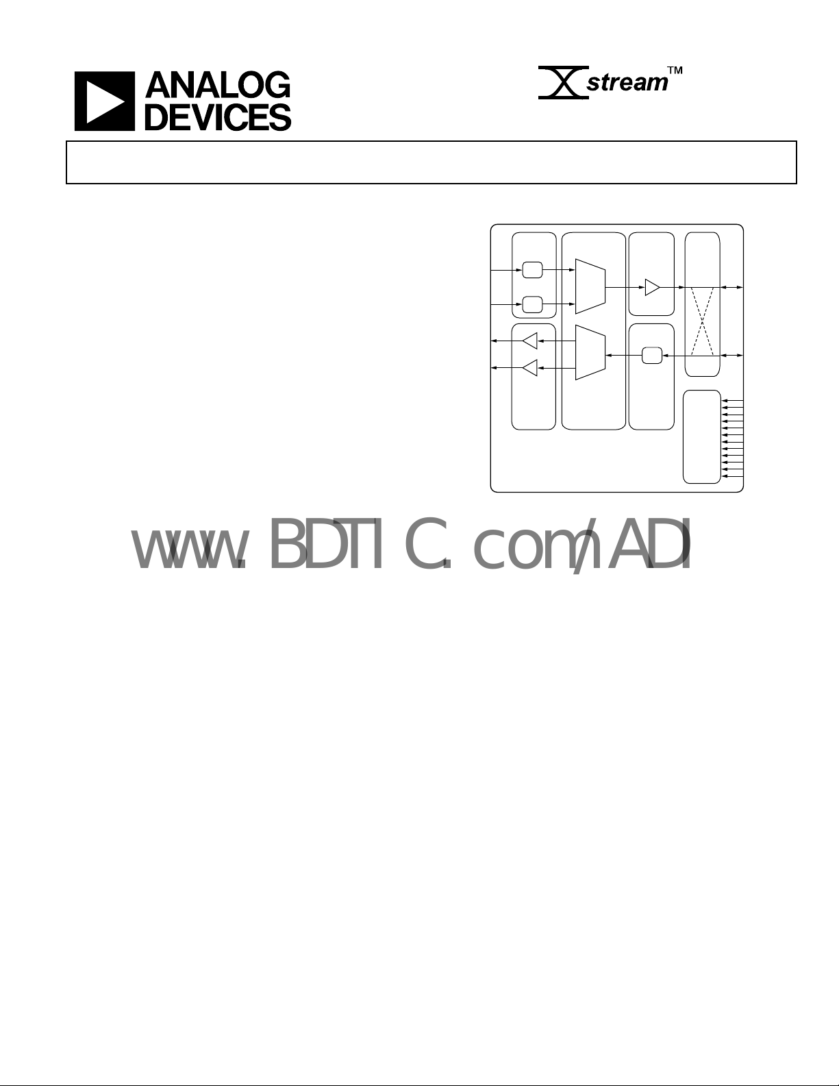
GENERAL DESCRIPTION
The AD8159 is an asynchronous, protocol agnostic, quad-lane
2:1 switch with a total of 12 differential PECL/CML-compatible
inputs and 12 differential CML outputs. The operation of this
product is optimized for NRZ signaling with data rates up to
3.2 Gbps per lane. Each lane offers two levels of input
equalization and four levels of output pre-emphasis.
-16
Quad Buffer Mux/Demux
AD8159
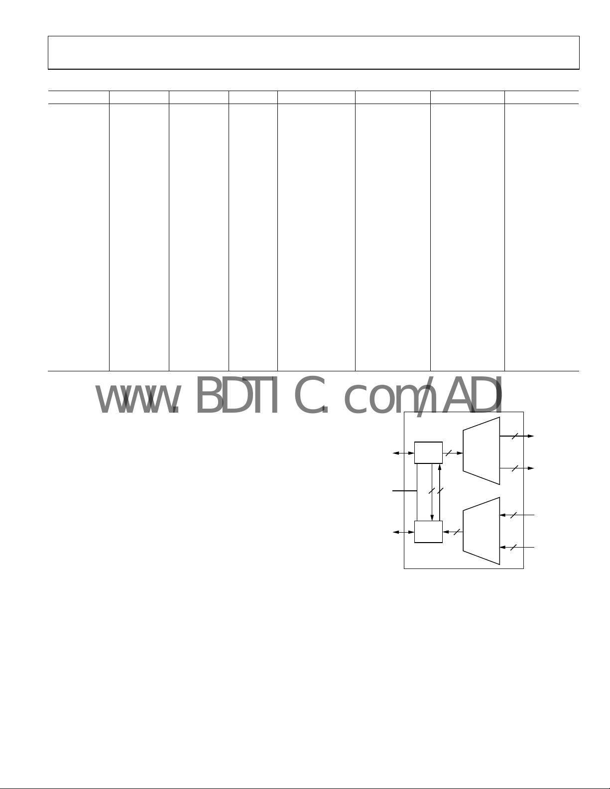
FUNCTIONAL BLOCK DIAGRAM
EQUALIZATION
Figure 1.
TRANSMIT
PRE-
EMPHASIS
EQ
RECEIVE
I/O
CROSS-
OVER
SWITCH
CONTROL
LOGIC
OUT_C[3:0]/
IN_C[3:0]
IN_C[3:0]/
OUT_C[3:0]
LB_A
LB_B
LB_C
PE_A[1:0]
PE_B[1:0]
PE_C[1:0]
EQ_A
EQ_B
EQ_C
SEL[3:0]
BICAST
REVERSE_C
RECEIVE
EQUALIZATION
IN_A[3:0]
IN_B[3:0]
OUT_A[3:0]
OUT_B[3:0]
EQ
EQ
TRANSMIT
PRE-
EMPHASIS
AD8159
2:1
1:2
QUAD
2:1
MULTIPLEXER/
1:2
DEMULTIPLEXER
The main application of the AD8159 is to support redundancy
on both the backplane side and the line interface side of a serial
link. The device has unicast and bicast capability, so it is
configurable to support either 1 + 1 or 1:1 redundancy.
The AD8159 supports reversing the output and input pins on
o
ne of its ports, which helps to connect two ASICs with
opposite pinouts.
05611-001
The AD8159 consists of four multiplexers and four demultip
lexers, one per lane. Each port is a 4-lane link, and each lane
runs up to a 3.2 Gbps data rate independent of the other lanes.
The lanes are switched independently using the four select pins,
The AD8159 is also used for testing high speed serial links by
uplicating incoming data and sending it to the destination port
d
and to test equipment simultaneously.
SEL[3:0]; each select pin controls one lane of the port. The
AD8159 has low latency and very low lane-to-lane skew.
Rev. A
Information furnished by Analog Devices is believed to be accurate and reliable. However, no
responsibility is assumed by Anal og Devices for its use, nor for any infringements of patents or ot her
rights of third parties that may result from its use. Specifications subject to change without notice. No
license is granted by implication or otherwise under any patent or patent rights of Analog Devices.
Trademarks and registered trademarks are the property of their respective owners.
One Technology Way, P.O. Box 9106, Norwood, MA 02062-9106, U.S.A.
Tel: 781.329.4700 www.analog.com
Fax: 781.461.3113 ©2006 Analog Devices, Inc. All rights reserved.

AD8159
www.BDTIC.com/ADI
TABLE OF CONTENTS
Features.............................................................................................. 1
Theory of Operation ...................................................................... 15
Applications....................................................................................... 1
General Description ......................................................................... 1
Functional Block Diagram .............................................................. 1
Revision History ............................................................................... 2
Specifications..................................................................................... 3
Absolute Maximum Ratings............................................................ 4
ESD Caution.................................................................................. 4
Pin Configuration and Function Descriptions............................. 5
Typical Performance Characteristics ............................................. 7
Evaluation Board Simplified Block Diagrams ............................ 12
Test Circuits..................................................................................... 13
REVISION HISTORY
4/06—Rev. 0 to Rev. A
Changes to Applications Section .................................................... 1
Changes to Table 5.......................................................................... 15
Updates to Outline Dimensions ...................................................22
Changes to Ordering Guide.......................................................... 22
Input Equalization (EQ) and Output Pre-Emphasis (PE).... 15
Loopback ..................................................................................... 16
Port C Reverse (Crossover) Capability.................................... 17
Applications..................................................................................... 18
Interfacing to the AD8159............................................................. 19
Termination Structures.............................................................. 19
Input Compliance....................................................................... 19
Output Compliance ................................................................... 20
Outline Dimensions....................................................................... 22
Ordering Guide .......................................................................... 22
9/05—Revision 0: Initial Version
Rev. A | Page 2 of 24

AD8159
www.BDTIC.com/ADI
SPECIFICATIONS
VCC = +3.3 V, VEE = 0 V, RL = 50 Ω, basic configuration,1 data rate= 3.2 Gbps, input common-mode voltage = 2.7 V, differential input
swing = 800 mV p-p, @ T
Table 1.
Parameter Conditions Min Typ Max Unit
DYNAMIC PERFORMANCE
Data Rate/Channel (NRZ) DC 3.2 Gbps
Deterministic Jitter Data rate = 3.2 Gbps; see Figure 21 20 ps p-p
Random Jitter RMS; see Figure 24 1 ps
Propagation Delay Input to output 600 ps
Lane-to-Lane Skew 100 ps
Switching Time 5 ns
Output Rise/Fall Time 20% to 80% 100 ps
INPUT CHARACTERISTICS
Input Voltage Swing Differential, V
Input Voltage Range Common mode, VID = 800 mV p-p;3 see Figure 25 VEE + 1.8 VCC + 0.3 V
Input Bias Current 4 μA
Input Capacitance 2 pF
OUTPUT CHARACTERISTICS
Output Voltage Swing Differential, PE = 0 800 mV p-p
Output Voltage Range Single-ended absolute voltage level; see Figure 26 VCC − 1.6 VCC + 0.6 V
Output Current Port A/B, PE_A/B = 0 16 mA
Port C, PE_C = 0 20 mA
Port A/B, PE_A/B = 3 28 mA
Port C, PE_C = 3 32 mA
Output Capacitance 2 pF
TERMINATION CHARACTERISTICS
Resistance Differential 90 100 110 Ω
Temperature Coefficient 0.15 Ω/°C
POWER SUPPLY
Operating Range
V
CC
Supply Current
I
CC
I
= I
+ I
TTO
TTOI
+ I
I/O
Supply Current
I
CC
I
= I
+ I
TTO
TTOI
+ I
I/O
THERMAL CHARACTERISTICS
Operating Temperature Range −40 +85 °C
θJA Still air 29 °C/W
θJB Still air 16 °C/W
θJC Still air 13 °C/W
LOGIC INPUT CHARACTERISTICS
Input High (VIH) 2.4 VCC V
Input Low (VIL) VEE 0.8 V
1
Bicast off, loopback off on all ports, pre-emphasis off on all ports, equalization set to minimum on all ports.
2
V
= input common-mode voltage.
ICM
3
VID = input differential peak-to-peak voltage swing.
= +25°C, unless otherwise noted.
A
VEE = 0 V 3.0 3.3 3.6 V
Basic configuration1, dc-coupled inputs/outputs, 400 mV I/O
swings (800 mV p-p differential), 50 Ω far end terminations
+ I
TTI
TTIO
BICAST = 1, PE = 3 on all ports, dc-coupled inputs/outputs,
400 mV I/O swings (800 mV p-p differential), 50 Ω far end
+ I
TTI
TTIO
terminations
= VCC − 0.6 V;2 see Figure 22 200 2000 mV p-p
ICM
175 mA
144 mA
255 mA
352 mA
Rev. A | Page 3 of 24

AD8159
www.BDTIC.com/ADI
ABSOLUTE MAXIMUM RATINGS
Table 2.
Parameter Rating
VCC to VEE 3.7 V
V
V
TTI
V
V
TTIO
V
V
TTO
V
V
TTOI
Internal Power Dissipation
Differential Input Voltage 2.0 V
Logic Input Voltage VEE − 0.3 V < VIN < VCC + 0.6 V
Storage Temperature Range
Lead Temperature
+ 0.6 V
CC
+ 0.6 V
CC
+ 0.6 V
CC
+ 0.6 V
CC
4.26 W
−65°C to +125°C
300°C
Stresses above those listed under Absolute Maximum Ratings
y cause permanent damage to the device. This is a stress
ma
rating only; functional operation of the device at these or any
other conditions above those indicated in the operational
section of this specification is not implied. Exposure to absolute
maximum rating conditions for extended periods may affect
device reliability.
ESD CAUTION
ESD (electrostatic discharge) sensitive device. Electrostatic charges as high as 4000 V readily accumulate on
the human body and test equipment and can discharge without detection. Although this product features
proprietary ESD protection circuitry, permanent damage may occur on devices subjected to high energy
electrostatic discharges. Therefore, proper ESD precautions are recommended to avoid performance
degradation or loss of functionality.
Rev. A | Page 4 of 24
AD8159
www.BDTIC.com/ADI
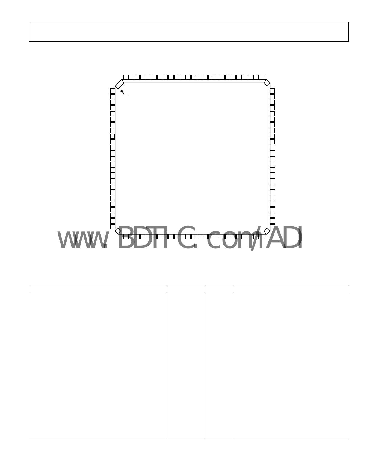
PIN CONFIGURATION AND FUNCTION DESCRIPTIONS
CC
EE
TTOI
EE
CC
EE
TTIO
EE
V
OIP_C098OIN_C097V
OIP_C195OIN_C194V
OIP_C292OIN_C291V
OIP_C389OIN_C388V
IOP_C086ION_C085V
IOP_C183ION_C182V
100
99
96
93
90
87
84
IOP_C280ION_C279V
81
IOP_C377ION_C376V
78
CC
1
NC
V
CC
V
EE
V
EE
V
EE
PE_A0
PE_A1
PE_B0
PE_B1
PE_C0
PE_C1
REVERSE_C
V
CC
ON_A3
OP_A3
V
EE
ON_A2
OP_A2
V
TTO
ON_A1
OP_A1
V
EE
ON_A0
OP_A0
V
CC
NC = NO CONNE CT
NOTES
1. THE AD8159 TQFP HAS AN EXPOSED PADDLE (ePAD) ON THE UNDERSIDE OF THE PACKAGE WHICH AIDS
IN HEAT DISS IPATIO N. THE ePAD M UST BE ELE CTRICALL Y CONNECTE D TO THE V
TO MEET THERMAL SPECIFICATIONS.
PIN 1
2
3
4
5
6
7
8
9
10
11
12
13
14
15
16
17
18
19
20
21
22
23
24
25
26
27
28
29
30
31
32
33
EE
CC
V
IP_A3
IN_A3
TTI
V
V
IP_A2
IN_A2
IN_A1
34
IP_A1
AD8159
TOP VIEW
(Not to Scale)
35
36
EE
V
IN_A0
37
38
39
40
41
42
43
44
45
46
47
48
EE
CC
V
V
IP_A0
OP_B3
ON_B3
OP_B2
ON_B2
EE
TTO
V
V
OP_B1
ON_B1
ON_B0
SUPPLY PLANE IN ORDER
EE
75
V
CC
74
EQ_A
73
EQ_B
72
EQ_C
71
SEL3
70
SEL2
69
SEL1
68
SEL0
67
LB_C
66
LB_B
65
LB_A
64
BICAST
63
V
CC
62
IP_B0
61
IN_B0
60
V
EE
59
IP_B1
58
IN_B1
57
V
TTI
56
IP_B2
55
IN_B2
54
V
EE
53
IP_B3
52
IN_B3
51
V
CC
49
50
CC
V
OP_B0
05611-002
Figure 2. Pin Configuration
Table 3. Pin Function Descriptions
Pin No. Mnemonic Type Description
1 NC N/A No connect
2, 13, 25, 26, 38, 50, 51, 63, 75, 76, 88, 100 VCC Power Positive supply
3 to 5, 16, 22, 29, 35, 41, 47, 54, 60, 79, 85, 91, 97 V
6 PE_A0 Control
7 PE_A1 Control
8 PE_B0 Control
9 PE_B1 Control
10 PE_C0 Control
11 PE_C1 Control
12 REVERSE_C Control
14 ON_A3 I/O
15 OP_A3 I/O
17 ON_A2 I/O
18 OP_A2 I/O
19, 44 V
20 ON_A1 I/O
21 OP_A1 I/O
23 ON_A0 I/O
24 OP_A0 I/O
Power Negative supply
EE
Pre-emphasis control for Port A (LSB)
Pre-emphasis control for Port A (MSB)
Pre-emphasis control for Port B (LSB)
Pre-emphasis control for Port B (MSB)
Pre-emphasis control for Port C (LSB)
Pre-emphasis control for Port C (MSB)
Reverse inputs and outputs on Port C
High speed output complement
High speed output
High speed output complement
High speed output
Power Port A and Port B output termination supply
TTO
High speed output complement
High speed output
High speed output complement
High speed output
27 IN_A3 I/O High speed input complement
Rev. A | Page 5 of 24
AD8159
www.BDTIC.com/ADI
Pin No. Mnemonic Type Description
28 IP_A3 I/O High speed input
30 IN_A2 I/O High speed input complement
31 IP_A2 I/O High speed input
32, 57 V
33 IN_A1 I/O High speed input complement
34 IP_A1 I/O High speed input
36 IN_A0 I/O High speed input complement
37 IP_A0 I/O High speed input
39 ON_B3 I/O High speed output complement
40 OP_B3 I/O High speed output
42 ON_B2 I/O High speed output complement
43 OP_B2 I/O High speed output
45 ON_B1 I/O High speed output complement
46 OP_B1 I/O High speed output
48 ON_B0 I/O High speed output complement
49 OP_B0 I/O High speed output
52 IN_B3 I/O High speed input complement
53 IP_B3 I/O High speed input
55 IN_B2 I/O High speed input complement
56 IP_B2 I/O High speed input
58 IN_B1 I/O High speed input complement
59 IP_B1 I/O High speed input
61 IN_B0 I/O High speed input complement
62 IP_B0 I/O High speed input
64 BICAST Control Bicast enable
65 LB_A Control Loopback enable for Port A
66 LB_B Control Loopback enable for Port B
67 LB_C Control Loopback enable for Port C
68 SEL0 Control
69 SEL1 Control
70 SEL2 Control
71 SEL3 Control
72 EQ_C Control Equalization control for Port C
73 EQ_B Control Equalization control for Port B
74 EQ_A Control Equalization control for Port A
77 ION_C3 I/O High speed input/output complement
78 IOP_C3 I/O High speed input/output
80 ION_C2 I/O High speed input/output complement
81 IOP_C2 I/O High speed input/output
82 V
83 ION_C1 I/O High speed input/output complement
84 IOP_C1 I/O High speed input/output
86 ION_C0 I/O High speed input/output complement
87 IOP_C0 I/O High speed input/output
89 OIN_C3 I/O High speed output/input complement
90 OIP_C3 I/O High speed output/input
92 OIN_C2 I/O High speed output/input complement
93 OIP_C2 I/O High speed output/input
94 V
95 OIN_C1 I/O High speed output/input complement
96 OIP_C1 I/O High speed output/input
98 OIN_C0 I/O High speed output/input complement
99 OIP_C0 I/O High speed output/input
Power Port A and Port B input termination supply
TTI
/B select for Lane 0
A
/B select for Lane 1
A
/B select for Lane 2
A
/B select for Lane 3
A
Power Port C input/output termination supply
TTIO
Power Port C output/input termination supply
TTOI
Rev. A | Page 6 of 24
AD8159
www.BDTIC.com/ADI
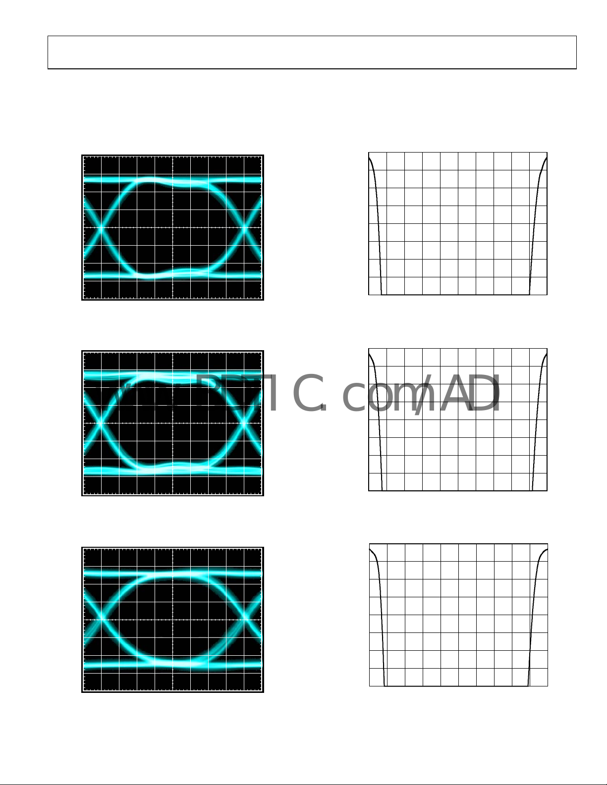
TYPICAL PERFORMANCE CHARACTERISTICS
VCC = +3.3 V, VEE = 0 V, RL = 50 Ω, basic configuration, data rate = 3.2 Gbps, input common-mode voltage = 2.7 V, differential input
swing = 800 mV p-p, T
Note: All graphs were generated using the setup shown in Figure 32, unless otherwise specified.
= 25°C, unless otherwise noted.
A
0
–2
–4
–6
–8
150mV/DIV
39.0625ps/DIV
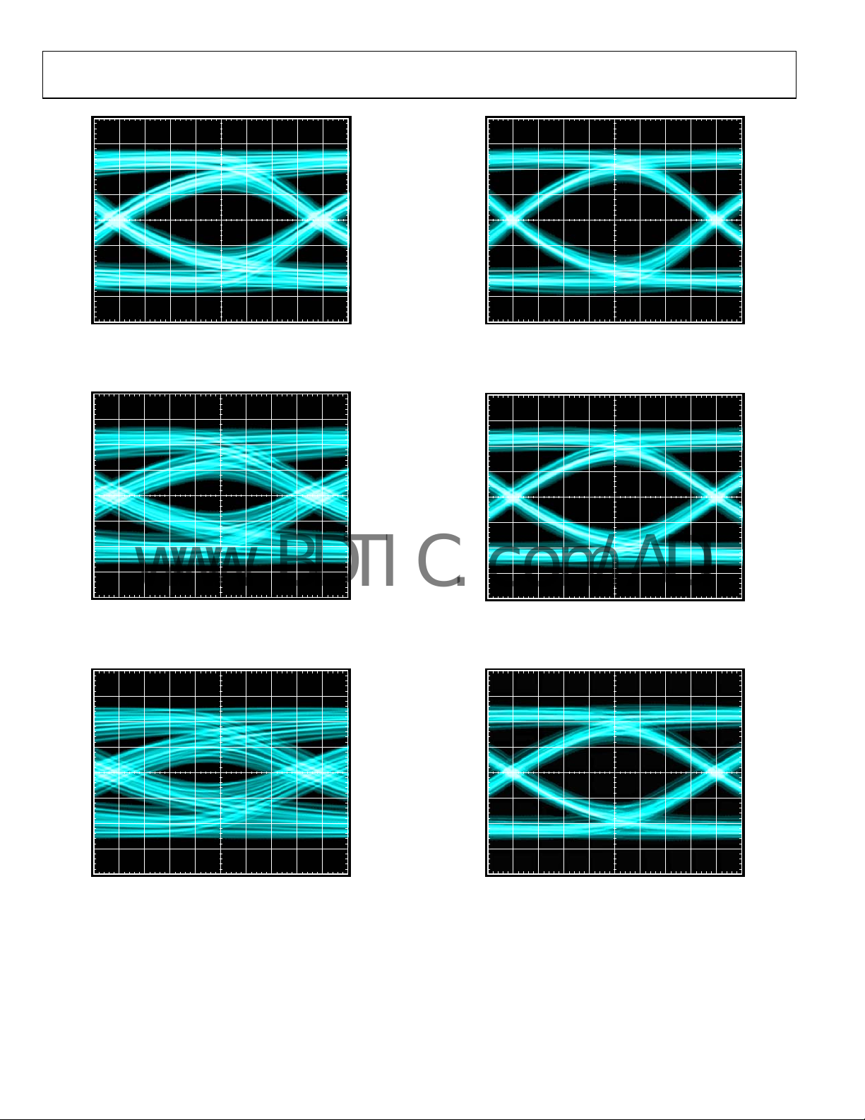
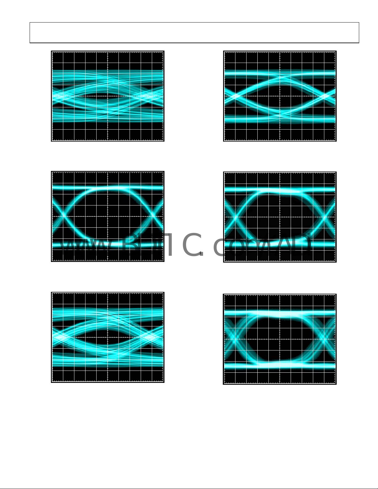
Figure 3. Output Port A Eye Diagram 3.2 Gbps
Input Port A or Input Port C
150mV/DIV
39.0625ps/DIV
Figure 4. Output Port B Eye Diagram
Input Port B
or Input Port C
05611-003
05611-004
–10
–12
BIT ERROR RATE (Decades)
–14
–16
0 1.0
0.1 0.2 0.3 0.4 0.5 0.6 0.7 0.8 0.9
TIME (Unit Interval)
Figure 6. Output Port A Bathtub Curve 3.2 Gbps
0
–2
–4
–6
–8
–10
–12
BIT ERROR RATE (Decades)
–14
–16
0 1.0
0.1 0.2 0.3 0.4 0.5 0.6 0.7 0.8 0.9
TIME (Unit Interval)
Figure 7. Output Port B Bathtub Curve 3.2 Gbps
0
05611-006
05611-007
–2
–4
–6
–8
150mV/DIV
39.0625ps/DIV
Figure 5. Output Port C Eye Diagram 3.2 Gbps
Input Port A
or Input Port B
05611-005
–10
–12
BIT ERROR RATE (Decades)
–14
–16
0.1 0.2 0.3 0.4 0.5 0.6 0.7 0.8 0.9
01
Figure 8. Output Port C Bathtub Curve 3.2 Gbps
Rev. A | Page 7 of 24
TIME (Unit Interval)
05611-008
.0
AD8159
www.BDTIC.com/ADI
150mV/DIV
39.0625ps/DIV
Figure 9. Eye Diagram over Backplane
(18
” FR4 + 2 GbX Connectors), PE = 0
150mV/DIV
Figure 10. Eye Diagram over Backplane
(30
” FR4 + 2 GbX Connectors), PE = 0
39.0625ps/DIV
05611-009
05611-044
150mV/DIV
39.0625ps/DIV
Figure 12. Eye Diagram over Backplane
(18
” FR4 + 2 GbX Connectors), PE = 1
150mV/DIV
Figure 13. Eye Diagram over Backplane
(30” FR4 + 2 GbX Connectors), PE = 2
39.0625ps/DIV
05611-012
05611-013
150mV/DIV
39.0625ps/DIV
Figure 11. Eye Diagram over Backplane
(36
” FR4 + 2 GbX Connectors), PE = 0
05611-011
150mV/DIV
39.0625ps/DIV
Figure 14. Eye Diagram over Backplane
(36
” FR4 + 2 GbX Connectors), PE = 3
Rev. A | Page 8 of 24
05611-014
AD8159
www.BDTIC.com/ADI
150mV/DIV
39.0625ps/DIV
Figure 15. Eye Diagram over Backplane
(42
” FR4 + 2 GbX Connectors), PE = 0
150mV/DIV
Figure 16. Reference Eye Diagram for Figure 19
39.0625ps/DIV
150mV/DIV
05611-015
Figure 18. Eye Diagram over Backplane
(42
150mV/DIV
05611-005
Figure 19. Eye Diagram with Equalization
Note: See Figure 34 for Test Circuit Used
39.0625ps/DIV
” FR4 + 2 GbX Connectors), PE = 3
39.0625ps/DIV
(10
” FR4), EQ = 0
05611-018
05611-016
150mV/DIV
39.0625ps/DIV
Figure 17. Reference Eye Diagram for Figure 20. Eye Diagram with Equalization
Figure 34 for Test Circuit Used
Figure 20
05611-044
150mV/DIV
” FR4 + 2 GbX Connectors), EQ = 1
(34
Note: See
Rev. A | Page 9 of 24
39.0625ps/DIV
05611-019

AD8159
www.BDTIC.com/ADI
100
90
80
70
60
50
40
30
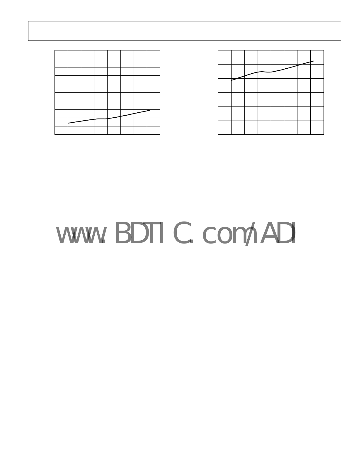
DETERMINISTIC JITTER (ps)
20
10
0
1.0 3.6
1.2 1.4 1.6 1.8 2.0 2.2 2.4 2.6 2.8 3.0 3.2 3.4
DATA RATE (Gbps)
Figure 21. Deterministic Jitter vs. Data Rate
100
VICM = 2.7V
90
80
70
60
INPUT C
50
40
30
DETERMINISTIC JITTER (ps)
INPUT A/B
20
10
0
0 2000
200 400 600 800 1000 1200 1400 1600 1800
DIFFERENTIAL INPUT SWING (mV p-p)
Figure 22. Deterministic Jitter v
s. Differential Input Swing
100
90
80
70
60
50
INPUT C
40
30
DETERMINISTIC JITTER (ps)
20
10
0
1.8 4.0
INPUT A/B
2.0 2.2 2.4 2.6 2.8 3.0 3.2 3.4 3.6 3.8
Figure 23. Deterministic Jitte
VCC (V)
r vs. Core Supply Voltage
05611-021
05611-024
05611-025
–2ps 0s–3ps 3ps
2ps–1ps 1ps
Figure 24. Random Jitter Histogram
Note: See
Figure 35 for Test Circuit Used
100
DIFFERENTIAL I NPUT SWI NG = 800mV p- p
90
80
INPUT A/B
70
60
50
40
30
DETERMINISTIC JITTER (ps)
20
10
0
04
0.5 1.0 1.5 2.0 2.5 3.0 3. 5
INPUT C
INPUT COMMON-MODE VOLTAGE (V)
Figure 25. Deterministic Jitter vs. Input Common-Mode Voltage
100
90
80
70
60
50
40
30
DETERMINISTIC JITTER (ps)
20
10
0
2.0 4.0
OUTPUT C
OUTPUT A/B
2.2 2.4 2.6 2.8 3.0 3.2 3.4 3.6 3.8
OUTPUT TERMINATION VOLTAGE (V)
Figure 26. Deterministic Jitter vs. Output Termination Voltage
05611-020
05611-023
.0
05611-026
Rev. A | Page 10 of 24
AD8159
www.BDTIC.com/ADI
100
90
80
70
60
50
40
30
DETERMINISTIC JITTER (ps)
20
10
0
–60 100
–40–200 20406080
TEMPERATURE (°C)
05611-022
Figure 27. Deterministic Jitter vs. Temperature
120
100
80
60
40
TRANSITION TIME (ps)
20
0
–60 100
–40–200 20406080
TEMPERATURE (°C)
Figure 28. Transition Time vs. Temperature
Note: See Figure 33 for Test Circuit Used
05611-027
Rev. A | Page 11 of 24

AD8159
www.BDTIC.com/ADI
EVALUATION BOARD SIMPLIFIED BLOCK DIAGRAMS
A
B
AD8159
AC-COUPLED
EVALUATIO N BOARD
C
AD8159-EVAL-AC
AC-COUPLED
EVALUATIO N BOARD
100Ω DIFF.
TRACE
0.1µF
100Ω DIFF.
C
A
B
TRACE
0.1µF
100Ω DIFF.
TRACE
0.1µF
5" 5"
INPUT A
INPUT B
INPUT C
V
TTI
V
TTIO
3.3V
/
VCCV
AD8159
V
EE
/
TTO
V
TTOI
OUTPUT C
OUTPUT A
OUTPUT B
100Ω DIFF.
TRACE
100Ω DIFF.
TRACE
100Ω DIFF.
TRACE
0.1µF
0.1µF
0.1µF
05611-028
Figure 29. AC-Coupled Evaluation Board Simplified Block Diagram
AD8159-EVAL-DC
DC-COUPLED
EVALUATIO N BOARD
/
A
B
AD8159
DC-COUPLED
EVALUATIO N BOARD
C
VCCV
V
TTI
V
TTIO
100Ω DIFF.
TRACE
100Ω DIFF.
C
A
B
TRACE
100Ω DIFF.
TRACE
5" 5"
INPUT A
INPUT B
INPUT C
AD8159
V
EE
–3.3V
Figure 30. DC-Coupled Evaluation Board Simplified Block Diagram
/
TTO
V
TTOI
OUTPUT C
OUTPUT A
OUTPUT B
100Ω DIFF.
TRACE
100Ω DIFF.
TRACE
100Ω DIFF.
TRACE
05611-029
Rev. A | Page 12 of 24

AD8159
T
www.BDTIC.com/ADI
TEST CIRCUITS
All graphs were generated using the setup shown in Figure 32, unless otherwise specified.
TERADYNE FR4 TEST BACKPLANE
GBX4 TO SMA DAUG HTER CARDS
0.25"
DIFFERENTIAL STRIPLINE TRACES
8mm WIDE, 8mm SPACE, 8mm HEIGHT
RACE LENGTHS = 6", 18", 24", 30" + 3" × 2 DAUGHTER CARDS
Figure 31. Test Backplane
05611-030
DATA OUT
PATTERN
GENERATOR
NOTES
1. SINGLE-ENDED REPRESENTATION
DATA OUT
PATTERN
GENERATOR
NOTES
1. SINGLE-ENDED REPRESENTATION
50Ω CABLE
50Ω CABLE
A
B
AD8159
AC-COUPLED
EVALUATIO N BOARD
C
A
B
AD8159
DC-COUPLED
EVALUATIO N BOARD
C
C
A
50Ω
B
50Ω
TEST BACKPLANE
Figure 32. AC-Coupled Test Circuit
C
A
B
50Ω CABLE
50Ω
50Ω
TEST BACKPLANE
Figure 33. DC-Coupled Test Circuit
No
te: Test Circuit Used for Figure 28
50Ω CABLE50Ω CABLE
50Ω CABLE
HIGH SPEED
REAL-TIME
OSCILLOSCOPE
50Ω
HIGH SPEED
REAL-TIME
OSCILLOSCOPE
50Ω
05611-031
05611-032
Rev. A | Page 13 of 24

AD8159
www.BDTIC.com/ADI
50Ω CABLE
DATA OUT
PATTERN
GENERATO R
NOTES
1. SINGLE-ENDED REPRESENTATION
A
B
C
C
AD8159
DC-COUPLED
EVALUATI ON BOARD
DATA OUT
PATTERN
GENERATOR
NOTES
1. SINGLE-ENDED REPRESENTATION
A
B
50Ω
No
te: Test Circuit Used for Figure 19 and Figure 20
50Ω CABLE
50Ω CABLE50Ω CABLE
TEST BACKP LANE
50Ω
Figure 34. Equalization Test Circuit
A
B
AD8159
AC-COUPLED
EVALUATIO N BOARD
C
50Ω CABLE
C
A
B
50Ω
Figure 35. Random Jitter Test Circuit
te: Test Circuit Used for Figure 24
No
DEVICE UNDER T EST
A
B
AD8159
DC-COUPLE D
EVALUATI ON BOARD
C
HIGH SPEED
SAMPLING
OSCILLOSCOPE
50Ω
50Ω
C
A
B
50Ω
50Ω CABLE
50Ω
05611-034
HIGH SPEED
REAL-TI ME
OSCILLOSCOPE
50Ω
05611-033
Rev. A | Page 14 of 24

AD8159
www.BDTIC.com/ADI
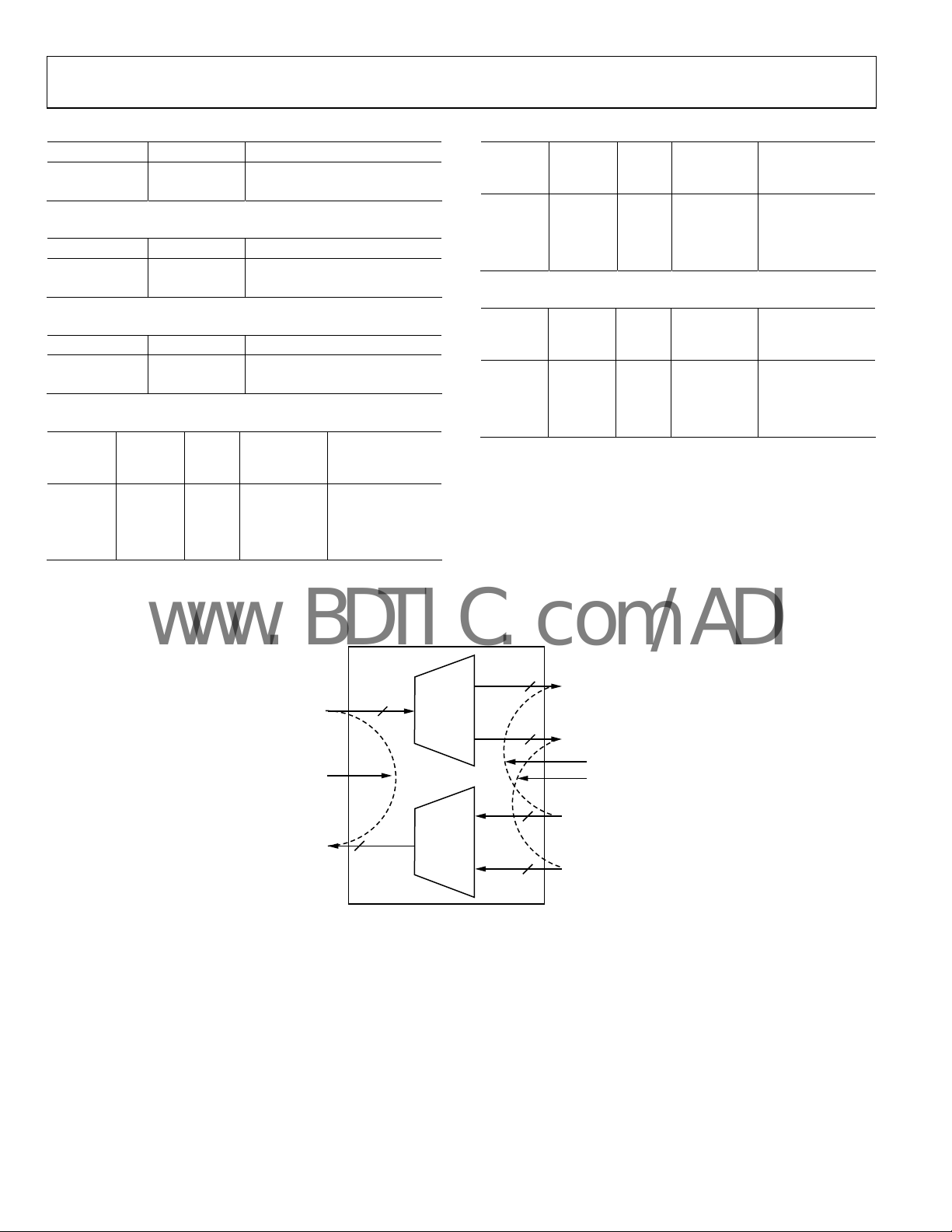
THEORY OF OPERATION
The AD8159 relays received data on the demultiplexer Input
Port C to Output Port A and/or Output Port B, depending on
the mode selected by the BICAST control pin. On the
multiplexer side, the AD8159 relays received data on either
Input Port A or Input Port B to Output Port C, based on the
SEL[3:0] pin states.
The AD8159 is configured by toggling control pins. On the demul-
iplexer side, when the device is configured in the unicast mode,
t
it sends the received data on Input Port C to Output Port A or
Output Port B. When the device is configured in the bicast mode,
received data on Input Port C is sent to both Output Port A and
Output Port B.
On the multiplexer side, only received data on Input Port A or
I
nput Port B is sent to Output Port C, depending on the state of
the SEL[3:0] pins. Tab l e 4 summarizes port selection and
c
onfiguration when loopback is disabled (LB_A = LB_B = LB_C
= 0).
When the device is in unicast mode, the output lanes on either
Po
rt A or Port B are in an idle state. In the idle state, the output
tail current is set to 0, and the P and N sides of the lane are
pulled up to the output termination voltage through the on-chip
termination resistors.
Table 4. Port Selection and Configuration Table
SEL BICAST OUT_A OUT_B OUT_C
0 0 IN_C Idle IN_A
0 1 IN_C IN_C IN_A
1 0 Idle IN_C IN_B
1 1 IN_C IN_C IN_B
Table 5. Port C I/O Selection
Port C when REVERSE_C = 0 Port C when REVERSE_C = 1 Port C Pin List on
100-Lead TQFP
77 ION_C3 = INN_C3 Input pin ION_C3 = OUTN_C3 Output pin
78 IOP_C3 = INP_C3 Input pin IOP_C3 = OUTP_C3 Output pin
80 ION_C2 = INN_C2 Input pin ION_C2 = OUTN_C2 Output pin
81 IOP_C2 = INP_C2 Input pin IOP_C2 = OUTP_C2 Output pin
83 ION_C1 = INN_C1 Input pin ION_C1 = OUTN_C1 Output pin
84 IOP_C1 = INP_C1 Input pin IOP_C1 = OUTP_C1 Output pin
86 ION_C0 = INN_C0 Input pin ION_C0 = OUTN_C0 Output pin
87 IOP_C0 = INP_C0 Input pin IOP_C0 = OUTP_C0 Output pin
89 OIN_C3 = OUTN_C3 Output pin OIN_C3 = INN_C3 Input pin
90 OIP_C3 = OUTP_C3 Output pin OIP_C3 = INP_C3 Input pin
92 OIN_C2 = OUTN_C2 Output pin OIN_C2 = INN_C2 Input pin
93 OIP_C2 = OUTP_C2 Output pin OIP_C2 = INP_C2 Input pin
95 OIN_C1 = OUTN_C1 Output pin OIN_C1 = INN_C1 Input pin
96 OIP_C1 = OUTP_C1 Output pin OIP_C1 = INP_C1 Input pin
98 OIN_C0 = OUTN_C0 Output pin OIN_C0 = INN_C0 Input pin
99 OIP_C0 = OUTP_C0 Output pin OIP_C0 = INP_C0 Input pin
Pin Name Input/Output Pin Name Input/Output
INPUT EQUALIZATION (EQ) AND OUTPUT PRE-EMPHASIS (PE)
In backplane applications, the AD8159 needs to compensate
for signal degradation over potentially long traces. The device
supports two levels of input equalization, configured on a perport basis.
gain (EQ) for each control setting as
of backplane trace that can be compensated for each setting.
The AD8159 also has four levels of output pre-emphasis,
configured for each port. The pre-emphasis circuitry adds
a controlled amount of overshoot to the output waveform
to compensate for the loss in a backplane trace.
Tabl e 9 to Ta bl e 11 summarize the high-frequency gain, amount
o
f overshoot, and the typical backplane channel length (including
two connectors) that can be compensated using each setting. A
typical backplane is made of FR4 material with 8 mil wide trace
and 8 mil spacing loosely coupled differential traces. Each
backplane channel consists of two connectors. The total length
of the channel includes three inches of traces on each card.
Table 6 to Table 8 summarize the high-frequency
well as the typical length
Rev. A | Page 15 of 24
AD8159
K
www.BDTIC.com/ADI
Table 6. IN_C Port Input Equalization Settings Table 10. OUT_A Port Output Pre-Emphasis Settings
EQ_C EQ Typical Backplane Length
0 6 dB 0 to 20 inches
1 12 dB 20 to 40+ inches
Table 7. IN_A Port Input Equalization Settings
EQ_A EQ Typical Backplane Length
0 6 dB 0 to 20 inches
1 12 dB 20 to 40+ inches
Table 8. IN_B Port Input Equalization Settings
EQ_B EQ Typical Backplane Length
0 6 dB 0 to 20 inches
1 12 dB 20 to 40+ inches
Table 9. OUT_C Port Output Pre-Emphasis Settings
Typical
plane
Back
PE_C[1] PE_C[0] PE Overshoot
Length
0 0 0 dB 0% 0 to 10 inches
0 1 1.9 dB 15% 10 to 20 inches
1 0 3.5 dB 35% 20 to 30 inches
1 1 4.9 dB 60% 30 to 40+ inches
PE_A[1] PE_A[0] PE Overshoot
0 0 0 dB 0% 0 to 10 inches
0 1 1.9 dB 15% 10 to 20 inches
1 0 3.5 dB 35%
1 1 4.9 dB 60% 30 to 40+ inches
Table 11. OUT_B Port Output Pre-Emphasis Settings
PE_B[1] PE_B[0] PE Overshoot
0 0 0 dB 0% 0 to 10 inches
0 1 1.9 dB 15% 10 to 20 inches
1 0 3.5 dB 35%
1 1 4.9 dB 60% 30 to 40+ inches
LOOPBACK
The AD8159 also supports port level loopback, illustrated in
Figure 36. The loopback control pins override the lane select
EL[3:0]) and bicast control (BICAST) pins. Tab l e 1 2 summa-
(S
r
izes the different loopback configurations.
Typ ic al
Backplane
Length
20 to 30 inches
Typ ic al
Backplane
Length
20 to 30 inches
IN_C[3:0]
PORT C LOOPBAC
OUT_C[3:0]
X4
X4
X4
Figure 36. Port-Based Loopback Cap
1:2 DEMUX
X4
X4
2:1 MUX
X4
ability
OUT_A[3:0]
OUT_B[3:0]
PORT A LOOPBACK
PORT B LOOPBACK
IN_A[3:0]
IN_B[3:0]
05611-035
Rev. A | Page 16 of 24
AD8159
www.BDTIC.com/ADI
Table 12. Loopback, Bicast, and Port Select Settings
1
LB_A LB_B LB_C SEL BICAST OUT_A OUT_B OUT_C
0 0 0 0 0 IN_C Idle IN_A
0 0 0 0 1 IN_C IN_C IN_A
0 0 0 1 0 Idle IN_C
0 0 0 1 1 IN_C IN_C
0 0 1 0 0 IN_C Idle
0 0 1 X 1 IN_C IN_C
0 0 1 1 0 Idle IN_C
0 1 0 0 X IN_C IN_B
0 1 0 1 0 Idle IN_B
0 1 0 1 1 IN_C IN_B
0 1 1 0 X IN_C IN_B
0 1 1 1 0 Idle IN_B
0 1 1 X 1 IN_C IN_B
1 0 0 0 0 IN_A Idle
1 0 0 0 1 IN_A IN_C
1 0 0 1 X IN_A IN_C
1 0 1 0 0 IN_A Idle
1 0 1 X 1 IN_A IN_C
1 0 1 1 X IN_A IN_C
1 1 0 0 X IN_A IN_B
1 1 0 1 X IN_A IN_B
IN_B
IN_B
IN_C
IN_C
IN_C
IN_A
IN_B
IN_B
IN_C
IN_C
IN_C
IN_A
IN_A
IN_B
IN_C
IN_C
IN_C
IN_A
IN_B
1 1 1 X X IN_A IN_B IN_C
1
Switching is done on a lane-by-lane basis, but input equalization, output pre-emphasis, and loopback are set for each port.
PORT C REVERSE (CROSSOVER) CAPABILITY
Port C has a reversible I/O capability. The sense (input vs.
output) of the Port C pins can be swapped by toggling the
REVERSE_C control pin. This feature has been added to
facilitate the connection to different ASICs that may have
the opposite pinouts.
Figure 37 illustrates the reversible I/O function of Port C, and
Tabl e 5 describes this function in a selection table that
co
rresponds to a TQFP-100 package. Please note that the
reverse capability is supported only on Port C.
IN_C [3:0]/OUT_C[3:0]
OUT_C [3:0]/IN_C[3:0]
X4
X4
I/O
SWITCH
X4REVERSE_C
I/O
SWITCH
Figure 37. Port C Reverse I/O Capability
X4
X4
1:2 DEMUX
X4
X4
2:1 MUX
X4
OUT_A[3:0]
OUT_B[3:0]
IN_A[3:0]
IN_B[3:0]
05611-036
Rev. A | Page 17 of 24
AD8159
www.BDTIC.com/ADI
APPLICATIONS
The main application of the AD8159 is to support redundancy
on both the backplane side and the line interface side of a serial
link. Each port consists of four lanes to support standards such
as XAUI.
sys
tem. Each line card is connected to two switch fabrics
(primary and redundant). The device can be configured to
support either 1 + 1 or 1:1 redundancy.
Another application for the AD8159 is test equipment for
eval
uating high speed serial I/Os running at data rates at or
lower than 3.2 Gbps. Figure 40 illustrates a possible application
o
f the AD8159 in a simple XAUI link tester.Figure 38 illustrates redundancy in an XAUI backplane
PHYSICAL
INTERFACE
PHYSICAL
INTERFACE
MACs
FRAMERS
MACs
FRAMERS
FABRIC INTERFACE
TRAFFIC MANAGERS
NETWORK PROCESSOR
FABRIC INTERFACE
TRAFFIC MANAGERS
NETWORK PROCESSOR
AD8159
LINE CARDS
AD8159
Figure 38. Using the AD8159 for Switch Redundancy
PRIMARY
MODULE
MACs
FRAMERS
REDUNDANT
MODULE
Figure 39. Using the AD8159 for Line Interface Redundancy
CONNECT TO DEVICE UNDER TEST
BACKPLANE
FABRIC INTERFACE
TRAFFIC MANAGERS
NETWORK PROCESSOR
LINE CARD
PRIMARY
SWITCH
FABRIC
REDUNDANT
SWITCH
FABRIC
FABRIC CARDS
05611-038
05611-037
CONNECTOR
PORT B
CONNECT TO PROTOCOL
ANALYZER
CONNECTOR
PORT A
PORT C
FPGA
GENERATES SIMPLE
PATTERNS
TEST CARD
05611-039
Figure 40. Using the AD8159 in Test Equipment
Rev. A | Page 18 of 24
AD8159
V
V
V
www.BDTIC.com/ADI
INTERFACING TO THE AD8159
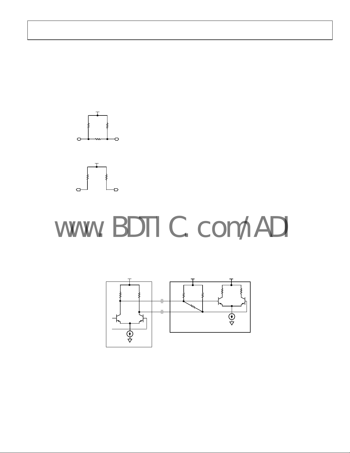
TERMINATION STRUCTURES
To determine the best strategy for connecting to the high speed
ins of the AD8159, the user must first be familiar with the on-
p
chip termination structures. The AD8159 contains two types of
these structures (see
and bidirectional ports and one type for output ports.
Figure 41. Termination Structure: Input and Bidirectional Ports
Figure 41 and Figure 42): one type for input
TTI/VTTIO/VTTOI
54.5Ω 54.5Ω
1173Ω
NP
05611-040
TTO
For output ports, there are two 50 Ω resistors connected to the
termination supply. Note that the differential input resistance
for both structures is the same, 100 Ω.
INPUT COMPLIANCE
The range of allowable input voltages is determined by the
damental limitations of the active input circuitry. This range
fun
of signals is normally a function of the common-mode level of
the input signal, the signal swing, and the supply voltage. For a
given input signal swing, there is a range of common-mode
voltages that keeps the high and low voltage excursions within
acceptable limits. Similarly, for a given common-mode input
voltage there is a maximum acceptable input signal swing.
There is also a minimum signal swing that the active input
circuitry can resolve reliably.
50Ω
PN
Figure 42. Output Ports
50Ω
05611-041
For input and bidirectional ports, the termination structure
consists of two 54.5 Ω resistors connected to a termination
supply and an 1173 Ω resistor connected across the differential
inputs, the latter being a result of the finite differential input
impedance of the equalizer.
CC
50Ω 50Ω
C
P
C
N
IP
1173Ω
IN
AD8159
Figure 22 and Figure 25 summarize the input voltage ranges for
all ports. Note that the input range is different when comparing
bidirectional ports to strictly input ports. This is a consequence
of the additional circuitry required to support the bidirectional
feature on Port C.
AC Coupling
One way to simplify the input circuit and make it compatible
with a wide variety of driving devices is to use ac coupling. This
has the effect of isolating the dc common-mode levels of the
driver and the AD8159 input circuitry. AC coupling requires a
capacitor in series with each single-ended input signal, as shown
in
Figure 43. This should be done in a manner that does not
in
terfere with the high speed signal integrity of the PCB.
V
TTI/VTTIO
54.5Ω
54.5Ω
V
VEE
CC
DRIVER
Figure 43. AC-Coupling Input Signal of AD8159
Rev. A | Page 19 of 24
05611-042
AD8159
V
www.BDTIC.com/ADI
When ac coupling is used, the common-mode level at the input
of the device is equal to V
swings above and below V
. The single-ended input signal
TTI
equally. The user can then use
TTI
Figure 22 and Figure 25 to determine the acceptable range of
c
ommon-mode levels and signal swing levels that satisfy the
input range of the AD8159.
If dc coupling is required, determining the input commonm
ode level is less straightforward because the configuration of
the driver must be also be considered. In most cases, the user
would set V
output termination voltage, V
on the AD8159 to the same level as the driver
TTI
. This prevents a continuous
TTOD
dc current from flowing between the two supply nets. As a
practical matter, both devices can be terminated to the same
physical supply net.
Consider the following example: A driver is dc-coupled to the
in
put of the AD8159. The AD8159 input termination voltage
(V
) and the driver output termination voltage (V
TTI
set to the same level; that is, V
TTI
= V
TTOD
= 3.3 V. If an 800 mV
) are both
TTOD
differential p-p swing is desired, the total output current of the
driver is 16 mA. At balance, the output current is divided evenly
between the two sides of the differential signal path, 8 mA to each
side. This 8 mA of current flows through the parallel combination of the 54.5 Ω input termination resistor on the AD8159
and the 50 Ω output termination resistor on the driver, resulting
in a common-mode level of
DC Coupling
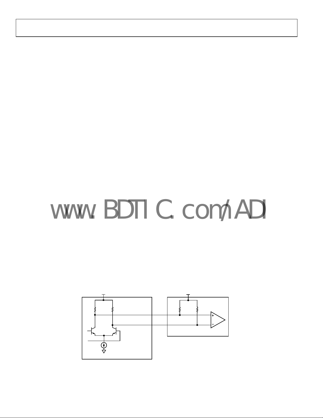
First, consider the dc-coupled case (see Figure 44). A lane on
utput Port A or Output Port B on the AD8159 is dc-coupled
O
to a receiving device. In this example, the output termination
voltage (V
input termination voltage (V
this level sets the high value (V
) on the AD8159 is set to the same level as the
TTO
) on the receiving device, and
TTIR
) of the single-ended output
HI
voltage. With pre-emphasis low (PE = 0), the maximum singleended current is 16 mA
1
, which flows through the parallel
combination of the 50 on-chip resistor and the 50 Ω far end
termination. Therefore, the low value (V
) of the output
LO
voltage is equal to
V
− 16 mA × (50 Ω || 50 Ω) = V
TTO
− 400 mV
TTO
Because the minimum allowed voltage at the output is
− 1.6 V, the lowest acceptable value for V
V
CC
V
− 1.6 V + 0.4 V = VCC − 1.2 V
CC
TTO
is
Increasing pre-emphasis to its highest level (PE = 3) results in
imum, single-ended current of 28 mA. In this case
a max
= V
V
LO
− 28 mA × (50 Ω || 50 Ω) = V
TTO
As a result, the lowest acceptable value for V
− 1.6 V + 0.7 V = VCC − 0.9 V
V
CC
2
− 700 mV
TTO
is
TTO
− 8 mA × (50 Ω || 54.5 Ω) = V
V
TTI
− 209 mV
TTI
The user can then use Figure 25 to determine the allowable
ra
nge of values for V
that meets the input compliance range
TTI
based on an 800 mV p-p differential swing.
OUTPUT COMPLIANCE
Not surprisingly, there is also a range of voltages that satisfies
the requirements of the output devices. This range is specified
as the minimum and maximum voltage (with respect to V
allowed at an output pin.
TTO
50Ω 50Ω
PORT A/B: ( 16 + 4 × PE) mA
PORT C: (20 + 4 × PE) mA
V
EE
Figure 44. DC-Coupling Output Signal from AD8159
)
CC
AD8159
OP
ON
It is expected that the minimum V
is 300 mV higher than the
TTO
case when PE = 0, because increasing the pre-emphasis level
results in a 300 mV lower voltage excursion at the output.
1
The output current for Port C when PE_C = 0 is slightly higher, 20 mA. The
extra 4 mA of current (compared to Port A/Port B) is needed to support the
bidirectional feature.
2
The output current for Port C when PE_C = 3 is 32 mA, for the same reason
as stated in Endnote 1.
V
TTIR
RECEIVING DE VICE
05611-043
Rev. A | Page 20 of 24

AD8159
www.BDTIC.com/ADI
AC Coupling
In general, more V
supply headroom is required with ac-
TTO
coupled outputs. When the outputs are ac-coupled, the average
single-ended current does not see the far end 50 Ω termination
because the capacitor acts as a dc block. For example, with
PE = 0, the single-ended output current alternates from 0 mA
to 16 mA, or 8 mA on average. This 8 mA current flows entirely
through the on-chip 50 Ω termination resistor due to the dc
block.
The single-ended output voltage has an average value of
V
− 8 mA × 50 Ω = V
TTO
For appropriate data patterns,
− 400 mV
TTO
1
the capacitor acts as a short and
the voltage swing is 400 mV p-p, identical to the dc-coupled case.
The low output voltage is, therefore,
− 400 mV − 200 mV = V
V
TTO
− 600 mV
TTO
1
AC coupling requires that the signal pattern have no long term dc
component. Codes such as 8b/10b, for example, ensure that the data
pattern is benign in an ac-coupled link.
The lowest acceptable value for V
V
− 1.6 V + 0.6 V = VCC − 1.0 V
CC
TTO
is
The same exercise can be repeated for other pre-emphasis
ttings.
se
Output Compliance Table
To simplify the task of interfacing to the AD8159 output,
Tabl e 13 is useful as a quick-reference. It provides the minimum
nd maximum values for output termination voltage for both
a
ac and dc coupling. The values in the table are valid for any preemphasis setting.
Table 13. Output Compliance
AC-Coupled DC-Coupled
V
TTO VCC
V
TTOI VCC
Minimum
(V)
– 0.5 VCC + 0.6 VCC – 0.9 VCC + 0.6
– 0.4 VCC + 0.6 VCC – 0.8 VCC + 0.6
Maximum
(V)
Minimum
(V)
Maximum
(V)
Rev. A | Page 21 of 24
AD8159
www.BDTIC.com/ADI
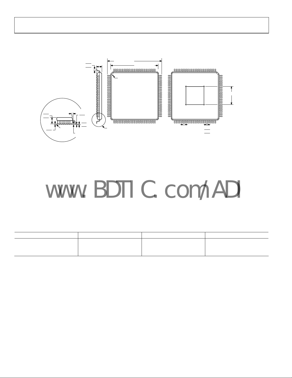
OUTLINE DIMENSIONS
1.05
1.00
0.95
0.15
SEATING
0.05
PLANE
VIEW A
ROTATED 90° CCW
1.20
0.75
MAX
0.60
0.45
0° MIN
0.20
0.09
7°
3.5°
0°
0.08 MAX
COPLANARIT Y
NOTES
1. CENTER FI GURES ARE TYPICAL UNL ESS OTHERWI SE NOTED.
2. THE AD8159 HAS A CONDUCTIVE HEAT SLUG TO HELP DISS IPATE HEAT AND ENSURE RELIABLE OPERATION OF
THE DEVICE O VER THE FULL INDUSTRIAL T EMPERATURE RANGE. THE SLUG IS EXPOSED ON T HE BOTTOM OF
THE PACKAGE AND ELECTRICALLY CONNECTED TO V
TRACES OR VIAS BE LOCATED UNDER THE PACKAGE THAT COULD COME IN CONTACT WITH THE CONDUCT IVE
SLUG. ATTACHING THE SLUG TO A V
DEVICE WHICH MAY BE BENEFICIAL IN HIG H TEMPERATURE ENVIRONME NTS.
Figure 45. 100-Lead Thin Quad Flat Packag
16.00 BSC SQ
1
PIN 1
25
26 50
VIEW A
COMPLIANT TO JEDEC STANDARDS MS-026-AED-HD
PLANE WILL REDUCE T HE JUNCTION T EMPERATURE OF THE
EE
14.00 BSC SQ
TOP VIEW
(PINS DOWN)
76100
. IT IS RECOMMENDED THAT NO PCB SIG NAL
EE
76 100
75
75
51
51
e, Exposed Pad [TQFP_EP]
EXPOSED
BOTTOM VIEW
0.50 BSC
LEAD PITCH
PAD
(PINS UP)
0.27
0.22
0.17
2650
(SV-100-4)
Dimensions shown in millimeters
1
5.00 SQ
25
040506-A
ORDERING GUIDE
Model Temperature Range Package Description Package Option
AD8159ASVZ −40°C to +85°C 100-Lead TQFP_EP SV-100-4
AD8159-EVAL-DC −40°C to +85°C DC-Coupled Evaluation Board
AD8159-EVAL-AC −40°C to +85°C AC-
1
Z = Pb-free part.
1
Coupled Evaluation Board
Rev. A | Page 22 of 24

AD8159
www.BDTIC.com/ADI
NOTES
Rev. A | Page 23 of 24

AD8159
www.BDTIC.com/ADI
NOTES
©2006 Analog Devices, Inc. All rights reserved. Trademarks and
registered trademarks are the property of their respective owners.
D05611-0-4/06(A)
Rev. A | Page 24 of 24
 Loading...