

6.25 Gbps, 4 × 4,
www.BDTIC.com/ADI
FEATURES
4 × 4, fully differential, nonblocking array
Configurable for dual 2 × 2 operation
DC to 6.25 Gbps per channel, NRZ data rate
Programmable input equalization compensates for over 40”
of FR-4 a
Multicast and broadcast modes of operation
Programmable output swing
100 mV p-p to 1.6 V p-p differential
Power supply: 3.3 V (±10%)
Low power
No EQ: 400 mW typical
Maximum EQ: 700 mW typical
Inputs: ac-coupled or dc-coupled
Wide set of dc-coupled input standards
3.3 V/2.5 V/1.8 V CML or 3.3 V LVPECL
Control: LVTTL- or LVCMOS-compatible
Low additive jitter: 25 ps p-p typical
Low random jitter: 0.8 ps rms
Integrated 50 Ω termination impedance at inputs/outputs
Individual output disable for power savings
49-ball, 8 mm × 8 mm BGA, 1 mm pitch
t 6.25 Gbps
Digital Crosspoint Switch with EQ
AD8156
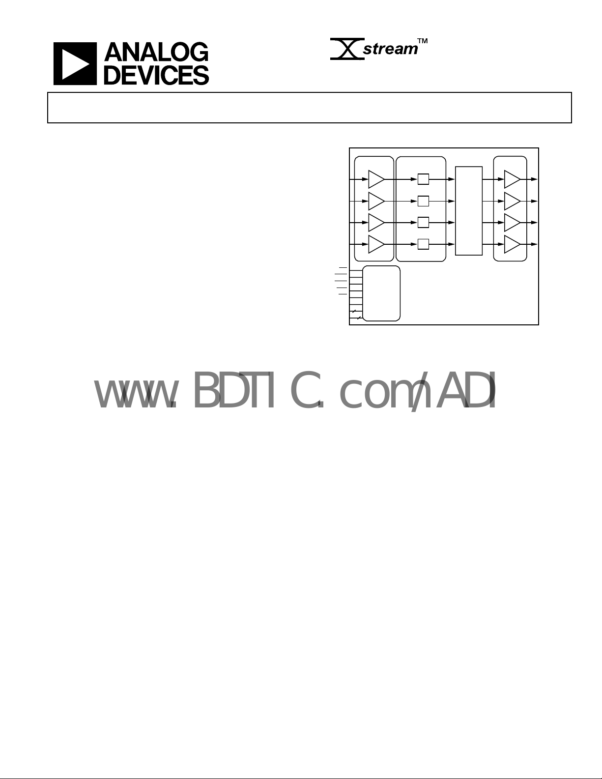
FUNCTIONAL BLOCK DIAGRAM
IN0P/N
IN1P/N
IN2P/N
IN3P/N
CS
RST
UPD
WE
RE
MODE
D[3:0]
A[3:0]
INPUT
RECEIVE RS
CONTROL
4
4
LOGIC
INPUT
EQUALIZATION
EQ
EQ
EQ
EQ
Figure 1.
AD8156
4 × 4
SWITCH
OUTPUT
DRIVERS
OUT0P/N
OUT1P/N
OUT2P/N
OUT3P/N
06305-001
APPLICATIONS
Backplane equalization
SONET/SDH
Gigabit Ethernet
XAUI
Fibre Channel
GENERAL DESCRIPTION
The AD8156, a member of the Xstream line of products, is a
high speed, fully differential, digital crosspoint switch. The part
can function as a 4 × 4 crosspoint switch with double-latched
memory, allowing simultaneous updates, or as a dual 2 × 2 with
direct output control. The AD8156 has low power dissipation,
typically 700 mW on 3.3 V with all outputs and input equalizers
active. It operates at any data rate from dc to 6.25 Gbps per port.
Each input channel on the AD8156 has a programmable input
qualizer to compensate for signal loss over a backplane.
e
The AD8156 high speed inputs are compatible with both ac-
upled and dc-coupled 3.3 V, 2.5 V, or 1.8 V CML, as well as
co
3.3 V LVPECL data levels. The control interface is LVTTL- and
LVCMOS-compatible at 3.3 V. All input and output termination
resistors are integrated for ease of layout and to minimize
impedance mismatch. Input equalization and unused outputs
can be individually disabled to minimize power dissipation.
The AD8156 is packaged in a 49-ball, 8 mm × 8 mm, BGA
ackage with a 1 mm ball pitch. It operates over the industrial
p
temperature range of −40°C to 85°C.
Rev. 0
Information furnished by Analog Devices is believed to be accurate and reliable. However, no
responsibility is assumed by Anal og Devices for its use, nor for any infringements of patents or ot her
rights of third parties that may result from its use. Specifications subject to change without notice. No
license is granted by implication or otherwise under any patent or patent rights of Analog Devices.
Trademarks and registered trademarks are the property of their respective owners.
One Technology Way, P.O. Box 9106, Norwood, MA 02062-9106, U.S.A.
Tel: 781.329.4700 www.analog.com
Fax: 781.461.3113 ©2007 Analog Devices, Inc. All rights reserved.

AD8156
www.BDTIC.com/ADI
TABLE OF CONTENTS
Features .............................................................................................. 1
Applications....................................................................................... 1
Functional Block Diagram .............................................................. 1
General Description......................................................................... 1
Revision History ............................................................................... 2
Specifications..................................................................................... 3
Electrical Specifications............................................................... 3
Timing Specifications .................................................................. 4
Timing Diagrams.............................................................................. 5
Absolute Maximum Ratings............................................................ 7
Thermal Resistance ...................................................................... 7
ESD Caution.................................................................................. 7
Pin Configurations and Function Descriptions ........................... 8
Typical Performance Characteristics ............................................. 9
Test Cir c ui t ...................................................................................... 12
Theory of Operation ...................................................................... 13
4 × 4 Mode................................................................................... 13
Dual 2 × 2 Mode......................................................................... 13
Input Equalization...................................................................... 14
Control Interface Description....................................................... 15
Control Pins................................................................................ 15
Address Pins, A[3:0] Inputs...................................................... 16
Data Pins, D[3:0] Inputs/Outputs............................................ 16
Control Interface Levels ............................................................ 16
Programming Examples ................................................................ 17
Dual 2 × 2 Mode (MODE Pin = 1)
Programming Examples............................................................ 17
4 × 4 Mode (MODE Pin = 0) Programming Examples ........ 17
Outline Dimensions ....................................................................... 19
Ordering Guide .......................................................................... 19
REVISION HISTORY
5/07—Revision 0: Initial Version
Rev. 0 | Page 2 of 20

AD8156
www.BDTIC.com/ADI
SPECIFICATIONS
ELECTRICAL SPECIFICATIONS
V
= V
TTI
V
= 1 V p-p differential, TA = 25°C, unless otherwise noted.
IN
Table 1.
Parameter Symbol Conditions Min Typ Max Unit
DYNAMIC PERFORMANCE
Maximum Data Rate NRZ data 6.25 Gbps
Deterministic Jitter Data date < 6.25 Gbps 25 ps p-p
Random Jitter 0.8 ps rms
Propagation Delay t
Propagation Delay Match 50 ps
Output Fall Time t
Output Rise Time tR Differential, 20% to 80% 75 ps
INPUT CHARACTERISTICS
Input Voltage Swing V
Input Voltage Range Single-ended VEE + 1.5 V
Input Voltage Range V
Input Termination R
OUTPUT CHARACTERISTICS
Output Voltage Swing V
Output Voltage Range Common-mode VEE + 1.6 V
Output Termination R
POWER SUPPLY
VCC Operating Range V
Supply Current I
I
I
I
I
Power Dissipation
All outputs on, no equalization 400 mW
All outputs and equalizers on 700 mW
THERMAL CHARACTERISTICS
Operating Temperature Range −40 85 °C
LOGIC INPUT CHARACTERISTICS VCC = 3.3 V dc
Input V
Input V
1
ICC supply current excludes input and output termination currents. Currents at V
output structure with separate termination supplies, all of the output and input current is drawn from V
2
Power dissipation includes power due to 800 mV p-p differential input and output voltages; this is the true representation of power dissipated on and used by the
chip at an 800 mV p-p differential signal level.
= VCC = 3.3 V, VEE = 0 V, RL = 50 Ω, differential output swing = 800 mV, ac-coupled, data rate = 6.25 Gbps, PRBS 223−1,
TTO
PD
F
IN
CM
IN
OUT
OUT
CC
1
CC
1
CC
1
CC
TTI
2
High 2.0 V
IN
Low 0 0.8 V
IN
TTO
All disabled 60 mW
Input to output 1000 ps
Differential, 20% to 80% 75 ps
Differential 200 2000 mV p-p
V
V
Common-mode VEE + 1.6 V
CC
CC
Single-ended 50 Ω
Differential, programmable 50 800 1850 mV p-p
CC
V
Single-ended 50 Ω
VEE = 0 V 3.0 3.3 3.6 V
All disabled 19 mA
All outputs on, no equalization 67 mA
All outputs and equalizers on 141 mA
800 mV differential swing 32 mA
800 mV differential swing 32 mA
V
and V
TTI
CC
count in power dissipation, but are not included in ICC. Note that in a CML
TTO
and the termination resistors, not from Vcc.
TTI
Rev. 0 | Page 3 of 20
AD8156
www.BDTIC.com/ADI
TIMING SPECIFICATIONS
V
= V
TTI
V
= 1 V p-p differential, TA = 25°C, unless otherwise noted.
IN
Table 2.
Parameter Symbol Min Typ Max Unit
FIRST RANK WRITE CYCLE
CS to WE Setup Time
Address Setup Time t
Data Setup Time t
WE to CS Hold Time
Address Hold Time t
Data Hold Time t
WE Pulse Width
SECOND RANK UPDATE CYCLE
CS to UPD Setup Time
UPD to CS Hold Time
Output Enable t
Output Switch t
Output Disable t
UPD Pulse Width
TRANSPARENT WRITE AND UPDATE CYCLE
Output Enable t
Output Toggle t
Output Disable t
SECOND RANK READBACK CYCLE
CS to RE Setup Time
RE to CS Hold Time
ADDR from RE
DATA from RE
Access Time t
RE to Read Disable
ASYNCHRONOUS RESET
Output Disable t
RST Pulse Width
= VCC = 3.3 V, VEE = 0 V, RL = 50 Ω, differential output swing = 800 mV, ac-coupled, data rate = 6.25 Gbps, PRBS 223 − 1,
TTO
t
t
t
t
t
t
t
t
t
t
t
t
CSW
ASW
DSW
CHW
AHW
DHW
WP
CSU
CHU
UOE
UOT
UOD
UW
WOE
WOT
WOD
CSR
CHR
RHA
RDE
AA
RDD
TOD
TW
0 ns
0 ns
1 ns
0 ns
0 ns
0 ns
10 ns
0 ns
0 ns
20 ns
10 ns
20 ns
10 ns
35 50 ns
25 45 ns
25 45 ns
0 ns
0 ns
5 ns
15 ns
15 30 ns
50 ns
10 25 ns
10 ns
Rev. 0 | Page 4 of 20
AD8156
A
www.BDTIC.com/ADI
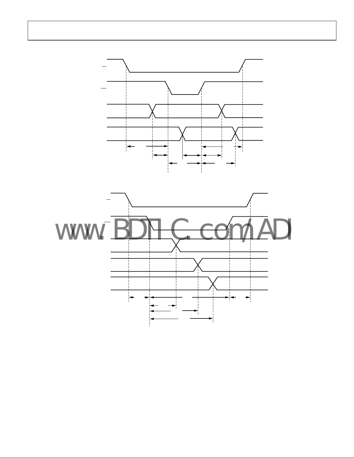
TIMING DIAGRAMS
CS
WE
[3:0]
D[3:0]
t
CSW
t
ASW
t
DSW
t
WP
t
AHW
t
DHW
t
CHW
06305-002
Figure 2. First Rank Write Cycle
CS
UPD
OUTxN/P
ENABLE
OUTxN/P
DISABLE
OUTxN/P
TOGGLE
t
UOD
t
UOT
t
UW
t
CHU
06305-003
t
CSU
t
UOE
Figure 3. Second Rank Update Cycle
Rev. 0 | Page 5 of 20
AD8156
www.BDTIC.com/ADI
CS
UPD
WE
OUTxN/P
ENABLE
OUTxN/P
DISABLE
OUTxN/P
TOGGLE
t
WOE
t
WOD
t
WOT
Figure 4. Transparent Write and Update Cycle
t
WHU
06305-004
CS
RE
ADDR[3:0]
DATA[3:0]
ADDR1 ADDR2
t
CSR
t
RDE
t
AA
DATA2DATA1
t
RHA
t
CHR
t
RDD
06305-005
Figure 5. Second Rank Readback Cycle
RST
OUTxN/P
DISABLE
t
TOD
t
TW
06305-006
Figure 6. Asynchronous Reset
Rev. 0 | Page 6 of 20

AD8156
www.BDTIC.com/ADI
ABSOLUTE MAXIMUM RATINGS
Table 3.
Parameter Rating
VCC to V
EE
V
TTI
V
TTO
Internal Power Dissipation
Input Voltage VCC + 0.6 V
Logic Input Voltage VEE − 0.3 V < VIN < VCC + 0.6 V
Storage Temperature Range −65°C to +125°C
Junction Temperature 150°C
Lead Temperature Range 300°C
1
Specification for TA = 25°C.
Stresses above those listed under Absolute Maximum Ratings
may cause permanent damage to the device. This is a stress
rating only; functional operation of the device at these or any
other conditions above those indicated in the operational
section of this specification is not implied. Exposure to absolute
maximum rating conditions for extended periods may affect
device reliability.
1
3.6 V
VCC + 0.6 V
VCC + 0.6 V
1.92 W
THERMAL RESISTANCE
θJA is specified for the worst-case conditions, that is, a device
soldered in a circuit board for surface-mount packages.
Table 4. Thermal Resistance
Package Type θ
49-Ball CSP_BGA 65 28 °C/W
JA
θ
JC
Unit
ESD CAUTION
Rev. 0 | Page 7 of 20

AD8156
www.BDTIC.com/ADI
PIN CONFIGURATIONS AND FUNCTION DESCRIPTIONS
7654321
A
CC
OUT0P
IN0NIN0PV
MODEV
CC
TTI
EE
IN1NIN1PV
D3V
V
EE
B
IN2PV
EE
C
IN2ND0D2RSTWECSOUT0N
V
TTO
OUT1P
OUT1N
EE
V
UPDV
CC
CC
V
EE
EE
OUT2NOUT2PV
Figure 7. Pin Configuration (Bottom View)
Table 5. Pin Function Descriptions
Pin No. Mnemonic Description
A1 V
EE
Negative Supply.
A2 IN1N High Speed Input Complement.
A3 IN1P High Speed Input.
A4 V
TTI
Input Termination Supply.
A5 IN0N High Speed Input Complement.
A6 IN0P High Speed Input.
A7 V
CC
Positive Supply.
B1 IN2P High Speed Input.
B2 V
EE
Negative Supply.
B3 D3 Input Address Pin (MSB).
B4 V
EE
Negative Supply.
B5 MODE Mode Select Pin.
B6 V
CC
Positive Supply.
B7 OUT0P High Speed Output.
C1 IN2N High Speed Input Complement.
C2 D0 Input Address Pin (LSB).
C3 D2 Input Address Pin.
C4
C5
C6
RST
WE
CS
Reset/Disable Outputs.
First Bank Write Enable.
Chip Select Enable.
C7 OUT0N High Speed Output Complement.
D1 V
D2 V
TTI
EE
Input Termination Supply.
Negative Supply.
D3 D1 Input Address Pin.
D4 V
EE
Negative Supply.
EE
EE
TTO
V
D1V
A2V
OUT3NOUT3PV
V
D
EE
CC
TTI
IN3PA0A1A3REV
E
IN3NV
F
V
G
CC
06305-007
Pin No. Mnemonic Description
D5
D6 V
D7 V
UPD
CC
TTO
Second Bank Write Enable.
Positive Supply.
Output Termination Supply.
E1 IN3P High Speed Input.
E2 A0 Address Pin (LSB).
E3 A1 Address Pin.
E4 A3 Address Pin (MSB).
E5
E6 V
RE
CC
Second Bank Read Enable.
Positive Supply.
E7 OUT1P High Speed Output.
F1 IN3N
F2 V
CC
High Speed Input Complement.
Positive Supply.
F3 A2 Address Pin.
F4 V
F5 V
F6 V
EE
EE
EE
Negative Supply.
Negative Supply.
Negative Supply.
F7 OUT1N High Speed Output Complement.
G1 V
CC
Positive Supply.
G2 OUT3N High Speed Output Complement.
G3 OUT3P High Speed Output.
G4 V
TTO
Output Termination Supply.
G5 OUT2N High Speed Output Complement.
G6 OUT2P High Speed Output.
G7 V
EE
Negative Supply.
Rev. 0 | Page 8 of 20

AD8156
V
V
V
V
V
V
www.BDTIC.com/ADI
TYPICAL PERFORMANCE CHARACTERISTICS
V
= V
TTI
V
= 1 V p-p differential, TA = 25°C, unless otherwise noted.
IN
= VCC = 3.3 V, VEE = 0 V, RL = 50 Ω, differential output swing = 800 mV, ac-coupled, data rate = 6.25 Gbps, PRBS 223 − 1,
TTO
200mV/DI
50ps/DIV
Figure 8. Input Eye Diagram at 3.2 Gbps,10” FR4
200mV/DI
50ps/DIV
Figure 9. Input Eye Diagram at 3.2 Gbps, 40” FR4
200mV/DI
06305-008
Figure 11. Output Eye Diagram at 3.2 Gbps, 10” FR4, Optimal EQ
200mV/DI
06305-009
Figure 12. Output Eye Diagram at 3.2 Gbps, 40” FR4, Optimal EQ
50ps/DIV
50ps/DIV
06305-011
06305-012
200mV/DI
06305-010
25ps/DIV
Figure 10. Input Eye Diagram at 6.25 Gbps, 10” FR4
Rev. 0 | Page 9 of 20
200mV/DI
Figure 13. Output Eye Diagram at 6.25 Gbps, 10” FR4, Optimal EQ
25ps/DIV
06305-013

AD8156
V
V
www.BDTIC.com/ADI
200mV/DI
25ps/DIV
Figure 14. Input Eye Diagram at 6.25 Gbps, 40” FR4
35
30
25
20
15
10
DETERMINI STIC JIT TER (ps p -p)
5
0
0
6.25Gbp s
3.2Gbps
1.00.5 2.01.5 2.5
DIFFERENTIAL INPUT (V p-p)
Figure 15. Deterministic Jitter vs. Input Si
gnal Level (No EQ)
200mV/DI
06305-014
25ps/DIV
06305-017
Figure 17. Output Eye Diagram at 6.25Gbps, 40” FR4, Optimal EQ
35
30
25
20
15
10
DETERMINISTIC JITTER (ps)
5
06305-015
0
–40 80
Figure 18. Deterministic Jitter vs. Te
6.25Gbp s
–20 604020
0
TEMPERATURE ( °C)
06305-019
mperature (Optimal EQ, 20” FR4)
35
30
25
20
15
10
DETERMINISTIC JITTER (ps p-p)
5
0
06
21543
INPUT DATA RATE (Gbps)
DETERMINISTIC
JITTER
06305-016
7
Figure 16. Deterministic Jitter vs. Data Rate (No EQ)
35
30
25
20
15
EQ GAIN (dB)
10
5
0
0.1 10
1
FREQUENCY (GHz)
Figure 19. Input EQ Gain vs. Frequency
06305-020
Rev. 0 | Page 10 of 20

AD8156
www.BDTIC.com/ADI
50
45
40
35
30
25
20
15
10
DETERMINISTIC JITTER (ps p-p)
5
0
3.0 3.1 3.2 3.3 3.4 3.5 3.6
VCC (V)
Figure 20. Deterministic Jitter vs. V
50
45
40
35
30
25
20
15
10
DETERMINISTIC JITTER (ps p-p)
5
0
0 0.5 1.0 1.5 2.0 2.5 3.0 3.5 4.0
OUTPUT TERMINATIO N VOLTAG E (V)
Figure 21. Deterministic Jitter vs. Output Termination Voltage
06305-022
CC
06305-023
800
700
600
500
400
300
EYE HEIGHT (mV)
200
100
0
01234567 98
DATA RATE (Gb ps)
06305-024
Figure 22. Eye Height vs. Data Rate
Rev. 0 | Page 11 of 20

AD8156
www.BDTIC.com/ADI
TEST CIRCUIT
AD8156
50Ω
CABLES
DATA OUT
PATTERN
GENERATOR
*SINGLE-ENDED REPRESENTATIO N
2 2 2 2
DIFFERENTIAL ST RIPLINE TRACES
8mils WIDE, 8mils SPACE,
AND 8mils DIELECTRIC HEIGHT
TRACE LENGTHS = 10", 20" , 30", AND 40"
FR4 TEST
BACKPLANE
50Ω
CABLES
AC-COUPLED
EVALUATIO N BOARD
IN0P/N
IN1P/N
IN2P/N
IN3P/N
OUT0P/N
OUT1P/N
OUT2P/N
OUT3P/N
Figure 23. AD8156 Test Circuit
2
2
2
2
50Ω
CABLES
2
50Ω
HIGH SPEED
SAMPLING
OSCILLOSCOPE
50Ω
50Ω50Ω
06305-021
Rev. 0 | Page 12 of 20

AD8156
www.BDTIC.com/ADI
THEORY OF OPERATION
The AD8156 is a 4 × 4 crosspoint switch with programmable
input equalization and programmable output current levels. It
can be used as a nonblocking and fully programmable 4 × 4
crosspoint switch, or as a dual 2 × 2 protection switch with fast
channel switching. Each lane can run at any rate from dc to
6.25 Gbps independent of the other lanes.
In 4 × 4 mode, the user writes the control data to double-latched
m
emory cells through a simple CPU interface. Connectivity,
individual output disables, output current level, and input equalization are all individually programmable. Broadcast addresses
can be used to simultaneously program the functionality of all
channels. A global reset disables the part and resets all equalizers
and output current levels to their default states. A chip select
pin can be used in applications where a single bus is controlling
multiple switches.
When in dual 2 × 2 mode, the part functions as two individual
2 × 2 swi
by the D3 to D0 pins, and output enable is controlled by the A3
to A0 pins. The dual 2 × 2 mode allows for sub-10 ns output
channel switching or output enable. Output swing control and
input equalization cannot be controlled in dual 2 × 2 mode
because all the data and address pins are used as asynchronous
control pins. However, settings are retained when switching modes,
so the user can set the desired swing and input equalization settings
in 4 × 4 mode on startup and then switch to dual 2 × 2 mode.
The user can switch at will between 4 × 4 mode and dual 2 × 2
m
mode to dual 2 × 2 mode, EQ and output current settings are
retained, but the output connectivity control is instantly
switched to the asynchronous interface of A[3:0] and D[3:0].
To have uninterrupted data flow when switching from 4 × 4
mode to dual 2 × 2 mode, the address and data pins should be
set into the desired states for dual 2 × 2 mode before changing
the MODE pin. When switching from dual 2 × 2 mode to 4 × 4
mode, EQ and the output current settings are also retained, but
the connectivity specified by the values of A[3:0] and D[3:0]
when MODE went low are retained in memory. Until some
other connectivity is set using the 4 × 4 control interface, the
last dual 2 × 2 mode settings are stored in memory.
tches whose connectivity is asynchronously controlled
ode by toggling the MODE pin. When switching from 4 × 4
4 × 4 MODE
Pulling the MODE pin low puts the AD8156 in 4 × 4 mode. In
this mode, the chip is controlled by the values stored in the onchip memory. This memory is organized as two banks of latches;
the second bank controls the chip, and the first bank allows the
next set of configuration data to be written while the chip is operating based on the second bank data. To write to the first bank of
memory, the user sets data and address to the desired states and
WE
pulls
configuration data is stored in the first bank of latches, and then the
chip configuration is simultaneously updated by pulling
low. This writing process is repeated until all desired
UPD
low.
Rev. 0 | Page 13 of 20
If desired for verification, the value of the second bank of
tches can be read back by pulling
la
Data Pin D3 to Data Pin D0 are driven by the chip. The timing
of this operation is shown in
ntirely asynchronous, the only limitation on the timing of the
e
read cycle is that each period must be a minimum of 15 ns.
RE
low. When RE is low,
Figure 5. Because the interface is
Connectivity Control
Connection between an output and an input is set by addressing
a specific output and connecting it to an input. Each output has
a disable bit. Tabl e 10 shows how to set the crosspoint
co
nnectivity.
Output Current Control
Output current is controlled by addressing a specific output and
choosing the output current. The output current is equal to
2 mA + (2 mA × D[3:
For example, the default code for D[3:0] is b0111. Therefore, the
utput current level is 2 mA + (2 mA × 7) = 16 mA. Table 1 1 and
o
Tabl e 13 show how to set the output current levels.
0])
Input Equalization Control
Input equalization is set per input lane. The equalization is
set in ~1.53 dB steps, from 0 dB to 23 dB of equalization at
3.125 GHz (roughly corresponding to a 6.25 Gbps bit rate).
The amount of equalization is
D[3:0]
15
×=
log40
fgain
)(
A value of 0000 disables the equalizer, saving power.
f
10
GHz83.0
Global Setting
By writing to one of three broadcast addresses, the user can set
all connectivity, output current, or input equalization settings to
the same value. Broadcast addresses are controlled similarly to
other control addresses. See
roadcast mode programming.
b
Tabl e 12 , Ta ble 1 3, and Tabl e 14 for
DUAL 2 × 2 MODE
Pulling the MODE pin high puts the AD8156 in dual 2 × 2
mode. In this mode, the part is asynchronously controlled by
the address and data pins, A[3:0] and D[3:0], respectively. In
dual 2 × 2 mode, the switch is configured as two individual 2 × 2
switches, and each output can be individually disabled. OUT0
and OUT1 can be connected to either IN0 or IN1, and OUT2
and OUT3 can connect to either IN2 or IN3. There are no
connectivity options in dual 2 × 2 mode to connect OUT0/OUT1
to IN2/IN3, or OUT2/OUT3 to IN0/IN1.
In dual 2 × 2 mode, input equalization and output level settings
a
re not accessible. If these functions are needed, the user should
program these functions in 4 × 4 mode and then return to dual
2 × 2 mode. Output swing and equalization settings are retained
from 4 × 4 mode to dual 2 × 2 mode. Readback is not available
in dual 2 × 2 mode.

AD8156
www.BDTIC.com/ADI
When in dual 2 × 2 mode, the A[3:0] and D[3:0] pins set the
AD8156 configuration state when
CS
is low. This configuration
method allows the user to have multiple AD8156s share the control
bus while each device has its own dedicated
AD8156
2 × 2
SWITCH
2 × 2
SWITCH
IN0P/N
IN1P/N
IN2P/N
IN3P/N
VCC
INPUT
RECEIVERS
MODE
INPUT
EQUALIZATION
EQ
EQ
EQ
EQ
Figure 24. AD8156 in Dual 2 × 2 Mode
CS
control signal.
OUTPUT
DRIVERS
OUT0P/N
OUT1P/N
OUT2P/N
OUT3P/N
INPUT EQUALIZATION
The AD8156 input equalization is an active scheme that is fully
linear over all operating ranges. The useful range of equalization
covers dc to 3.125 GHz frequencies or dc to 6.25 Gbps data
rates. Other key features include:
• 15 s
• Ga
teps of gain, linear in dB, programmable through the
4 × 4 control interface
in has a 40 dB per decade slope
6305-008
• P
eak gain of 23 dB at 3.125 GHz (~6.25 Gbps)
• E
qualizes more than 40” of typical FR4 backplane with
associated connectors and vias at all speeds
• 0.10 UI p-p r
• 0.15 UI p-p r
esidual deterministic jitter typ @ 3.125 Gbps
esidual deterministic jitter typ @ 6.25 Gbps
As with all equalizers, the gain setting is the key. The ideal
m
ethod of choosing the proper gain setting is to run the equalizer
with the channel, and choose the setting with minimum jitter.
If this process is not possible or is too time consuming for the
number of channels required, the loss of the channel at
3.125 GHz should be measured. The best equalizer setting is
usually 2 dB to 4 dB more than the loss at 3.125 GHz. Using the
40 dB slope of the equalizer gain, the gain at other frequencies
can be calculated based on the peak gain at 3.125 GHz. The
formula to use is
f
10
GHz83.0
where f i
D[3:0]
15
×=
log40
fgain
)(
s the fundamental frequency of the data, or the data
rate divided by 2 (that is, 6.25 Gbps → f = 3.125 GHz).
Performance of the equalizer is heavily dependent on the channel
us
ed. Operation at high speeds depends on features such as
dielectric used (for example, FR4, Nelco3000, or Rogers), connector
quality, via stub length, and routing geometry and topology.
Rev. 0 | Page 14 of 20

AD8156
www.BDTIC.com/ADI
CONTROL INTERFACE DESCRIPTION
The control interface for the AD8156 consists of a set of
address, data, and several control pins. All control pins are
active low. The control interface is level sensitive.
CONTROL PINS
All control pins on the chip are level-sensitive, not edge-triggered.
The preferred programming method is to assert the data and
address pins to their desired configuration, wait one control bit
period, then pull
After one control bit period,
additional control bit period, the address and data pins can be
set to their next values, and the cycle repeats. Using this
method, each write takes three control bit periods.
After the first bank of registers is programmed,
which transfers the data from the first bank of latches to the second
bank of latches. When
regardless of the status of the address, data,
Writ i ng t o the p ar t whi l e
first bank of registers and into the second bank, immediately
affecting the connectivity and output current of the part. It is
recommended that the user write to the first bank with one data
bit cycle, and subsequently activate the
data and address pin skews presented to the part can lead to
errors when writing through both banks simultaneously. If
skews are properly controlled, a transparent write can allow a
very quick change of states in 4 × 4 mode.
Pin
RST
At any time, a reset pulse to
interface to globally reset all first and second bank latches to
their default values. The device has an internal power-on reset
circuit, but it is recommended that
power-up. The default values for the chip include disabling all
outputs, turning off equalization, and setting output current code to
the default, b0111 (16 mA). The default connection is the buffer
state, or IN0 → OUT0, IN1 → OUT1, IN2 → OUT2, IN3 → OUT3;
WE
low to write to the first bank of registers.
WE
is pulled high. After an
UPD
is pulled low,
UPD
is pulled low, the full chip updates,
WE
, or RE pins.
UPD
is pulled low writes through the
UPD
pin low, because
RST
can be applied to the control
RST
be held low during
all outputs are connected but disabled.
other control pins.
Pin
CS
The chip select pin, an active low signal, facilitates multiple chip
address decoding. All control signals, except the reset signal, are
ignored when
and does not affect operation of the chip.
any of the latches, preserving any data programmed in the latches.
CS
is pulled high. The pin disables the control signals
MODE Pin
The MODE pin sets the part in 4 × 4 mode or dual 2 × 2 mode.
Pulling MODE low sets the part in 4 × 4 mode, and pulling
MODE high sets the part in dual 2 × 2 mode. In dual 2 × 2
mode, the
WE
This pin is the write enable to the first bank of registers. Forcing
WE
in the first bank of latches for the function specified by A[3:0].
The
changing the other pins after a write cycle to avoid overwriting
the first bank data.
UPD
This pin is the write enable to the second bank of registers.
Forcing
bank latches to the second bank latches, which is the active set
of registers. The chip functions update during this operation.
RE
This pin is the read enable for the second bank of registers.
Forcing
bidirectional D[3:0] pins. The on-chip drivers are only intended
to drive high impedance loads, so any external drivers of D[3:0]
must be disabled when
WE
, RE, and
Pin
to logic low allows the data on the D[3:0] pins to be stored
WE
pin must be returned to logic high state before
Pin
UPD
to logic low transfers the data stored in all first
Pin
RE
to logic low enables the on-chip drivers to drive the
UPD
pins are unused.
RE
is low.
RST
overrides all of the
CS
does not power down
Table 6. Basic Control Pin Functions
RST CS
1 1 x x x x
0 x x x x x Global Reset. Disables all outputs and equalizers. Output current code set to 0111 (16 mA).
1 0 0 1 1 1
1 0 0 0 1 1 Write Enable. Writes to the first bank of registers.
1 0 0 1 0 1 Readback Enable. Reads back data on D[3:0] from the addressed latch (second bank of registers).
1 0 0 1 x 0
1 0 0 0 x 0
1 0 1 x x x Dual 2 × 2 Mode. Address and data pins asynchronously control the device.
MODE
WE
RE UPD
Functio n
Control Interface Disabled. Prior settings are stored, and the chip is run based on the
onfiguration data stored (in 4 × 4 mode) or set (in dual 2 × 2 mode) previously.
c
4 × 4 Mode. Address and data pins are ignored (values in the AD8156 memory control connectivity,
output curr
Global Update. Transfers data from first bank of registers to second bank of registers (active set).
Chip func
Transparent Write. Writes and updates simultaneously thr
registers. Chip functions update.
ent, and EQ setting).
tions update.
Rev. 0 | Page 15 of 20
ough first bank to the second bank of

AD8156
www.BDTIC.com/ADI
ADDRESS PINS, A[3:0] INPUTS
The AD8156 feature sets can be set port by port or globally.
A[3:2] specify what is being programmed or read back when
the part is being configured port by port. Connectivity, output
current, equalization, or global programming features are
chosen based on the values of A[3:2]. Similarly, A[1:0] address
the port that is being programmed or read back. In global
programming, A[1:0] serve a different function. Refer to
Tab l e 1 5 for programming examples.
to
Table 7. Dual 2 × 2 Mode Programming Table
Address A[3:0] Data D[3:0]
Input A3 to Input A0 enable Output 3 to Output 0, respectively. Input D3 to Input D0 control the connectivity of Output 3 to Output 0, respectively.
1 = Enables the output (for all A[3:0] inputs) 0 = Input 2, 1 = Input 3 (for D2 and D3)
0 = Disables the output (for all A[3:0] inputs) 0 = Input 0, 1 = Input 1 (for D0 and D1)
Table 8. 4 × 4 Mode Programming Table
Mode Address A[3:0] Data D[3:0]
Write/Read Connectivity
and Disable
Write/Read Output
Current Level
Broadcast
Connectivity/Disable
Broadcast Output
Current Level
Broadcast EQ Setting 1 0 1 1 D3 D2 D1 D0
Program EQ Setting 1 1 A1 A0 D3 D2 D1 D0
0 0 A1 A0 0 D2 D1 D0
A1 and A0 determine which
output is being pr
0 1 A1 A0 D3 D2 D1 D0
A1 and A0 determine which
output is being programmed.
1 0 0 0 0 D2 D1 D0
1 0 0 1 D3 D2 D1 D0
A1 and A0 determine which
put is being programmed.
in
ogrammed.
Tabl e 9
D1 and D0 determine which input is connected to which output;
D2 determines the enabled/disabled state of that output, with D2 = 1
(enable). When writing or reading, D3 is always 0.
D0 to D3 binarily program the output current level/voltage swing with the
output current = 2 mA + (2 mA × decimal (D[3:0])).
D1 and D0 determine which input is connected to all of the outputs.
D2 determines the enabled/disabled state of all outputs with D2 = 1 (enable).
When writing or reading, D3 is always 0.
D0 to D3 binarily program the output current level/voltage swing with the
utput current = 2 mA + (2 mA × decimal (D[3:0])). The value is written to
o
all outputs.
Data inputs D0 to D3 set the input
Gain(f) = D[3:0]/15 × 40 log
D0 to D3 set the input equalization level, where:
Gain(f) = D[3:0]⁄15 × 40 log
DATA PINS, D[3:0] INPUTS/OUTPUTS
In readback mode, the D[3:0] pins are low impedance outputs
indicating the stored values in the memory to be read. The
readback drivers are designed to drive high impedances only,
so external drivers connected to D[3:0] must be disabled during
readback mode.
CONTROL INTERFACE LEVELS
The AD8156 control interface shares the data path supply pins,
V
and VEE. The potential between the positive logic supply
CC
and the negative supply VEE must be at least 3.0 V and no
V
CC
more than 3.7 V. Regardless of supply, the logic threshold is
approximately one-half the supply range, allowing the interface
to be used with most LVCMOS- and LVTTL-logic drivers.
equalization level where:
(f/0.83 GHz).
10
(f⁄0.83 GHz).
10
Rev. 0 | Page 16 of 20

AD8156
www.BDTIC.com/ADI
PROGRAMMING EXAMPLES
A[3:0]
D[3:0]
WE
UPD
Figure 25. Sample Timing Diagram for 4x4 Mode Programming Examples
06305-009
DUAL 2 × 2 MODE (MODE PIN = 1) PROGRAMMING EXAMPLES
Table 9. Dual 2 × 2 Mode Programming
Address Pins Data Pins
A3 A2 A1 A0 D3 D2 D1 D0 Description
1 0 0 0 0 x x x A[3] = 1 enables OUT3. D[3] = 0 connects IN2 to OUT3.
1 0 0 0 1 x x x A[3] = 1 enables OUT3. D[3] = 1 connects IN3 to OUT3.
1 1 0 0 0 0 x x A[3:2] = b11 enables OUT2 and OUT3. D[3:2] = b00 connects IN2 to both OUT2 and OUT3.
1 1 0 0 1 0 x x
0 0 1 0 x x 0 x A[1] = 1 enables OUT1. D[1] = 0 connects IN0 to OUT1.
0 0 1 1 x x 1 1 D[1:0] = b11 enables OUT0 and OUT1. D[1:0] = b11 connects IN1 to both OUT0 and OUT1.
1 1 1 1 0 1 0 1
A[3:2] = b11 enables OUT2 and OUT3. D[3:2] = b10 connects IN2 to OUT2 and connects IN3
3.
to OUT
A[3:0] = b1111 enables all outputs. D[3:0] = b0101 c
OUT1, IN1 to OUT0.
onnects IN2 to OUT3, IN3 to OUT2, IN0 to
4 × 4 MODE (MODE PIN = 0) PROGRAMMING EXAMPLES
Table 10. Connectivity Programming, A[3:2] = b00
Address Pins Data Pins
A3 A2 A1 A0 D3 D2 D1 D0 Description
0 0 0 0 0 1 0 0 A[1:0] = 0 selects OUT0. D2 = 1 enables OUT0. D[1:0] = 0 connects IN0 to OUT0.
0 0 0 0 0 0 0 0 A[1:0] = 0 selects OUT0. D2 = 0 disables OUT0. D[1:0] = 0 connects IN0 to OUT0.
0 0 1 0 0 1 0 1 A[1:0] = b10 selects OUT2. D2 = 1 enables OUT2. D[1:0] = b01 connects IN1 to OUT2.
0 0 1 1 0 1 0 0 A[1:0] = b11 selects OUT3. D2 = 1 enables OUT3. D[1:0] = b00 connects IN0 to OUT3.
Table 11. Output Level Programming, A[3:2] = b01
Address Pins Data Pins
A3 A2 A1 A0 D3 D2 D1 D0 Description (Output Current = 2 mA + (2 mA × D[3:0])
0 1 0 0 0 1 0 0 A[1:0] = 0 selects OUT0. D[3:0] = b0100 sets OUT0 current to 2 mA + (2 mA × 4) = 10 mA.
0 1 0 0 1 0 0 0 A[1:0] = 0 selects OUT0. D[3:0] = b1000 sets OUT0 current to 2 mA + (2 mA × 8) = 18 mA.
0 1 1 0 1 1 0 1 A[1:0] = b10 selects OUT2. D[3:0] = b1101 sets OUT2 current to 2 mA + (2 mA × 13) = 28 mA.
0 1 1 1 0 0 0 0 A[1:0] = b11 selects OUT3. D[3:0] = b0000 sets OUT3 current to 2 mA + (2 mA × 0) = 2 mA.
Rev. 0 | Page 17 of 20

AD8156
www.BDTIC.com/ADI
Table 12. Broadcast Connectivity Programming, A[3:0] = b1000
Address Pins Data Pins
A3 A2 A1 A0 D3 D2 D1 D0 Description
1 0 0 0 0 1 0 0 D2 = 1 enables all outputs. D[1:0] = b00 connects IN0 to all outputs.
1 0 0 0 0 1 1 1 D2 = 1 enables all outputs. D[1:0] = b11 connects IN3 to all outputs.
1 0 0 0 0 0 1 0
D2 = 0 disables all outputs. D[1:0] = b10 c
outputs are disabled.
onnects IN2 to all outputs, but all
Table 13. Broadcast Output Level Program
Address Pins Data Pins
A3 A2 A1 A0 D3 D2 D1 D0 Description (Output Current = 2 mA + (2 mA × D[3:0])
1 0 0 1 0 1 0 0 D[3:0] = b0100 sets current of all outputs to 2 mA + (2 mA × 4) = 10 mA.
1 0 0 1 1 1 0 1 D[3:0] = b1101 sets current of all outputs to 2 mA + (2 mA × 13) = 28 mA.
1 0 0 1 0 0 0 0 D[3:0] = b0000 sets current of all outputs to 2 mA + (2 mA × 0) = 2 mA.
Table 14. Broadcast Equalization (EQ) Programming, A
Address Pins Data Pins
A3 A2 A1 A0 D3 D2 D1 D0 Description (Gain(f) = D[3:0]⁄15 × 40 log10(f⁄0.83 GHz)), assume f = 2.25 GHz
1 0 1 1 0 1 0 0 D[3:0] = b0100 sets all input EQ = (4/15 × 40 log10(2.25 GHz/0.83 GHz)) = 4.6 dB.
1 0 1 1 1 1 0 1 D[3:0] = b1101 sets all input EQ = (13/15 × 40 log10(2.25 GHz/0.83 GHz)) =14.95 dB.
1 0 1 1 0 0 0 0 D[3:0] = b0000 sets all input EQ = (0/15 × 40 log10(2.25 GHz/0.83 GHz)) = 0 dB.
Table 15. Individual Input EQ Programming, A[3:2] = b11
Address Pins Data Pins
A3 A2 A1 A0 D3 D2 D1 D0 Description (Gain(f) = D[3:0]⁄15 × 40log10(f⁄0.83 GHz)), assume f = 2.25 GHz
1 1 0 0 0 1 0 0
1 1 0 1 1 1 0 1
1 1 1 0 1 1 1 1
1 1 1 1 0 0 0 0
ming, A[3:0] = b1001
[3:0] = b1011
A[1:0] = b00 selects IN0.
D[3:0] = b0100 s
A[1:0] = b01 selects IN1.
D[3:0] = b1101 s
A[1:0] = b10 selects IN2.
D[3:0] = b1111 s
A[1:0] = b11 selects IN3.
D[3:0] = b0000 s
ets EQ = (4/15 × 40 log
ets EQ = (13/15 × 40 log
ets EQ = (15/15 × 40 log
ets EQ = (0/15 × 40 log
(2.25 GHz/0.83 GHz)) = 4.6 dB.
10
(2.25 GHz/0.83 GHz)) = 14.95 dB.
10
(2.25 GHz/0.83 GHz)) = 17.25 dB.
10
(2.25 GHz/0.83 GHz)) = 0 dB.
10
Rev. 0 | Page 18 of 20

AD8156
*
www.BDTIC.com/ADI
OUTLINE DIMENSIONS
1.85
1.71
1.50
8.20
8.00 SQ
7.80
BALL A1
PAD CORNER
TOP VIEW
DETAIL A
6.00
BSC SQ
0.25
MIN
63
745
1.00
BSC
0.70
0.60
0.50
BALL DIAMETER
A1 CORNER
INDEX AREA
BOTTOM
VIEW
DETAILA
2
1
SEATING
PLANE
A
B
C
D
E
F
G
*
1.31
1.21
1.10
COPLANARITY
0.20
*
COMPLIANT WITH JEDEC STANDARDS MO-192-ABB-1
WITH EXCEPTION TO PACKAGE HEIGHT AND THICKNESS.
Figure 26. 49-Ball Chip Scale Package Ball Grid Array [CSP_BGA]
(BC-49-3)
Dimensions shown in millimeters
012006-0
ORDERING GUIDE
Model Temperature Range Package Description Package Option
AD8156ABCZ
AD8156-EVALZ
1
Z = RoHS Compliant Part.
1
−40°C to +85°C 49-Ball Chip Scale Package Ball Grid Array [CSP_BGA] BC-49-3
1
Evaluation Board
Rev. 0 | Page 19 of 20

AD8156
www.BDTIC.com/ADI
NOTES
© 2007 Analog Devices, Inc. All rights reserved. Trademarks and
registered trademarks are the property of their respective owners.
D06305-0-5/07(0)
Rev. 0 | Page 20 of 20
 Loading...