

Page 1
www.BDTIC.com/ADI
3.2 Gbps
FEATURES
Single lane 2:1 mux/1:2 demux
3.2 Gbps to dc data rates
Compensates over 40 inches of FR4 at 3.2 Gbps through
Two levels of input equalization, or
Four levels of output pre-emphasis
Operates with ac- or dc-coupled differential I/O
Low deterministic jitter, typically 16 ps p-p
Low random jitter, typically 500 fs rms
On-chip terminations
Unicast or bicast on 1:2 demux function
Loopback capability on all ports
3.3 V core supply
Flexible I/O supply
Low power, typically 200 mW in basic configuration
32-lead LFCSP package
−40°C to +85°C operating temperature range
APPLICATIONS
Low cost redundancy switch
SONET OC48/SDH16 and lower data rates
Gigabit Ethernet over backplane
Fibre Channel 1.06 Gbps and 2.12 Gbps over backplane
Serial RapidIO
PCI Express Gen 1
Infiniband over backplane
1
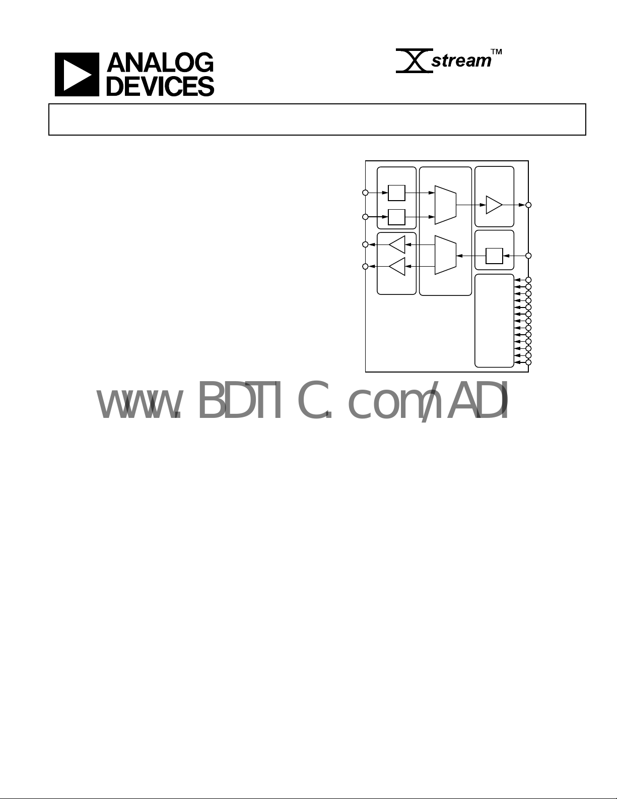
Single Buffered Mux/Demux Switch
AD8153
FUNCTIONAL BLOCK DIAGRAM
TRANSMIT
PRE-EMPHASIS
RECEIVE
EQUALIZATION
EQ
CONTROL
LOGIC
OUTPUT C
INPUT C
SEL
BICAST
LB_A
LB_B
LB_C
MODE
RESETB
EQ_A/(SCL)
EQ_B/(SDA)
EQ_C
PE_A/(I2C_A[0])
PE_B/(I2C_A[1])
PE_C/(I2C_A[2])
INPUT A
INPUT B
OUTPUT A
OUTPUT B
RECEIVE
EQUALIZATION
EQ
EQ
TRANSMIT
PRE-EMPHASIS
2:1 MULTIPLEXER/
1:2 DEMULTIPLEXE R
AD8153
Figure 1.
06393-001
GENERAL DESCRIPTION
The AD8153 is an asynchronous, protocol agnostic, single-lane
2:1 switch with three differential CML inputs and three differential
CML outputs. The AD8159, another member of the Xstream
line of products, is suitable for similar applications that require
more than one lane.
The AD8153 is optimized for NRZ signaling with data rates of
up to 3.2 Gbps per port. Each port offers two levels of input
equalization and four levels of output pre-emphasis.
The device consists of a 2:1 multiplexer and a 1:2 demultiplexer.
There are three operating modes: pin mode, serial mode, and
mixed mode. In pin mode, lane switching, equalization, and
pre-emphasis are controlled exclusively using external pins. In
serial mode, an I
Rev. 0
Information furnished by Analog Devices is believed to be accurate and reliable. However, no
responsibility is assumed by Anal og Devices for its use, nor for any infringements of patents or ot her
rights of third parties that may result from its use. Specifications subject to change without notice. No
license is granted by implication or otherwise under any patent or patent rights of Analog Devices.
Trademarks and registered trademarks are the property of their respective owners.
2
C interface is used to control the device and to
provide access to advanced features, such as additional preemphasis settings and output disable. In mixed mode, the user
2
accesses the advanced features using I
C, but controls lane
switching using the external pins.
The main application of the AD8153 is to support redundancy
on both the backplane side and the line interface side of a serial
link. The device has unicast and bicast capability, so it is capable
of supporting either 1 + 1 or 1:1 redundancy.
Using a mixture of bicast and loopback modes, the AD8153 can
also be used to test high speed serial links by duplicating the
incoming data and transmitting it to the destination port and
test equipment simultaneously.
1
Two ports active with no pre-emphasis.
One Technology Way, P.O. Box 9106, Norwood, MA 02062-9106, U.S.A.
Tel: 781.329.4700 www.analog.com
Fax: 781.461.3113 ©2007 Analog Devices, Inc. All rights reserved.
Page 2

AD8153
www.BDTIC.com/ADI
TABLE OF CONTENTS
Features.............................................................................................. 1
Applications....................................................................................... 1
Functional Block Diagram .............................................................. 1
General Description ......................................................................... 1
Revision History ............................................................................... 2
Specifications..................................................................................... 3
2
I
C Timing Specifications............................................................ 4
Absolute Maximum Ratings............................................................ 5
ESD Caution.................................................................................. 5
Pin Configuration and Function Descriptions............................. 6
Typical Performance Characteristics ............................................. 7
Theory of Operation ...................................................................... 13
Switch Configurations ............................................................... 13
Receive Equalization .................................................................. 14
Transmit Pre-Emphasis............................................................. 14
2
I
C Serial Control Interface........................................................... 15
Register Set.................................................................................. 15
General Functionality................................................................ 15
2
I
C Data Write............................................................................. 16
2
I
C Data Read.............................................................................. 17
Applications Information.............................................................. 18
PCB Design Guidelines ................................................................. 19
Interfacing to the AD8153............................................................. 20
Termination Structures.............................................................. 20
Input Compliance....................................................................... 20
Output Compliance ................................................................... 21
Outline Dimensions....................................................................... 22
Ordering Guide .......................................................................... 22
REVISION HISTORY
4/07—Revision 0: Initial Version.
Rev. 0 | Page 2 of 24
Page 3

AD8153
www.BDTIC.com/ADI
SPECIFICATIONS
VCC = V
pattern, V
Table 1.
Parameter Conditions Min Typ Max Unit
DYNAMIC PERFORMANCE
Data Rate/Channel (NRZ) DC 3.2 Gbps
Deterministic Jitter Data rate = 3.2 Gbps, high EQ 16 ps p-p
Random Jitter RMS, high EQ 500 fs
Propagation Delay Input to output 640 ps
Lane-to-Lane Skew 55 ps
Switching Time 5 ns
Output Rise/Fall Time 20% to 80% 85 ps
INPUT CHARACTERISTICS
Input Voltage Swing Differential 200 2000 mV p-p
Input Voltage Range Common mode, VID = 800 mV p-p VEE + 1.0 VCC + 0.3 V
Input Capacitance 2 pF
OUTPUT CHARACTERISTICS
Output Voltage Swing Differential, @ dc 700 800 900 mV p-p
Output Voltage Range Single-ended absolute voltage level Vcc − 1.6 Vcc + 0.6 V
Output Current No pre-emphasis 16 mA
Output Current Maximum pre-emphasis, all ports 28 mA
Output Capacitance 2 pF
TERMINATION CHARACTERISTICS
Resistance Differential 100 Ω
Temperature Coefficient 0.1 Ω/°C
POWER SUPPLY
Operating Range
Supply Current
Supply Current
THERMAL CHARACTERISTICS
Operating Temperature Range −40 +85 °C
θJA Still air 30.0 °C/W
LOGIC INPUT CHARACTERISTICS
Input High (VIH) 2.4 VCC V
Input Low (VIL) VEE 0.8 V
1
VID: Input differential voltage swing.
= V
TTI
V
CC
V
V
TTI
V
V
TTO
= 3.3 V, VEE = 0 V, RL = 50 Ω, two outputs active with no pre-emphasis, data rate = 3.2 Gbps, ac-coupled, PRBS7 test
TTO
= 800 mV p-p, TA = 25°C, unless otherwise noted.1
ID
VEE = 0 V 3.0 3.3 3.6 V
= 0 V VCC V
EE
= 0 V VCC V
EE
Two outputs active, no pre-emphasis, 400 mV I/O swings
I
CC
I
= I
+ I
I/O
TTO
TTI
(800 mV p-p differential)
Three outputs active, maximum pre-emphasis, 400 mV
I
CC
I
= I
+ I
I/O
TTO
TTI
I/O swings (800 mV p-p differential)
27 31 35 mA
26 32 39 mA
53 58 63 mA
74 84 95 mA
Rev. 0 | Page 3 of 24
Page 4
AD8153
www.BDTIC.com/ADI
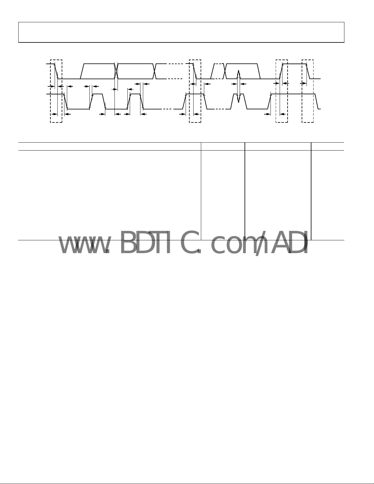
I2C TIMING SPECIFICATIONS
SDA
t
BUF
SPSrS
06393-006
SCL
SU;STO
t
r
t
HD;STA
HIGH
t
f
Figure 2. I
t
SU;STA
2
C Timing Diagram
t
t
HD;DAT
SU;DAT
t
t
f
t
LOW
t
HD;STA
t
r
t
SP
t
Table 2.
Parameter Symbol Min Max Unit
SCL Clock Frequency f
Hold Time for a Start Condition t
Set-up Time for a Repeated Start Condition t
Low Period of the SCL Clock t
High Period of the SCL Clock t
Data Hold Time t
Data Set-Up Time t
Rise Time for Both SDA and SCL t
Fall Time for Both SDA and SCL t
Set-Up Time for Stop Condition t
Bus Free Time Between a Stop Condition and a Start Condition t
Capacitance for Each I/O Pin C
0 400+ kHz
SCL
HD;STA
SU;STA
LOW
HIGH
HD;DAT
SU;DAT
r
f
SU;STO
BUF
i
0.6 – μs
0.6 – μs
1.3 – μs
0.6 – μs
0 – μs
10 – ns
1 300 ns
1 300 ns
0.6 – μs
1 – ns
5 7 pF
Rev. 0 | Page 4 of 24
Page 5
AD8153
www.BDTIC.com/ADI
ABSOLUTE MAXIMUM RATINGS
Table 3.
Parameter Rating
VCC to VEE 3.7 V
V
V
TTI
V
V
TTO
Internal Power Dissipation
Differential Input Voltage 2.0 V
Logic Input Voltage V
Storage Temperature Range
Lead Temperature
Junction Temperature
+ 0.6 V
CC
+ 0.6 V
CC
4.1 W
− 0.3V < V
EE
−65°C to +125°C
300°C
150°C
< VCC + 0.6 V
IN
Stresses above those listed under Absolute Maximum Ratings
y cause permanent damage to the device. This is a stress
ma
rating only; functional operation of the device at these or any
other conditions above those indicated in the operational
section of this specification is not implied. Exposure to absolute
maximum rating conditions for extended periods may affect
device reliability.
ESD CAUTION
Rev. 0 | Page 5 of 24
Page 6
AD8153
www.BDTIC.com/ADI
PIN CONFIGURATION AND FUNCTION DESCRIPTIONS
)
E_C/(I2C_A[2])
OPC
INC
PE_A/(I2C_A[0]
IPC
29
31
30
PIN 1
INDICATOR
AD8153
TOP VIEW
11
12
10
PB
VCC
O
ONB
ONC
PE_B/(I2C_A[1])
P
28
27
26
25
24 MODE
23 RESETB
22 SEL
21 BICAST
20 LB_A
19 LB_B
18 LB_C
17 EQ_A/(SCL )
15
16
14
13
IPB
INB
EQ_C
EQ_B/(SDA)
06393-002
VEE
32
1VCC
2VTTO
3ONA
4OPA
5VTTI
6INA
7IPA
8VEE
9
VCC
NOTE
EPAD NEEDS TO BE ELECTRICALLY
CONNECTED TO VEE.
Figure 3. Pin Configuration
Table 4. Pin Function Descriptions
Pin No. Mnemonic Type Description
1, 9, 12 VCC Power Positive Supply.
2 VTTO Power Output Termination Supply.
3 ONA I/O High Speed Output Complement.
4 OPA I/O High Speed Output.
5 VTTI Power Input Termination Supply.
6 INA I/O High Speed Input Complement.
7 IPA I/O High Speed Input.
8, 32, EPAD VEE Power Negative Supply.
10 ONB I/O High Speed Output Complement.
11 OPB I/O High Speed Output.
13 INB I/O High Speed Input Complement.
14 IPB I/O High Speed Input.
15 EQ_C Control Port C Input Equalization Control.
16 EQ_B/(SDA) Control Port B Input Equalization Control/(I2C Data when MODE = 1).
17 EQ_A/(SCL) Control Port A Input Equalization Control/(I2C Clock when MODE = 1).
18 LB_C Control Port C Loopback Enable.
19 LB_B Control Port B Loopback Enable.
20 LB_A Control Port A Loopback Enable.
21 BICAST Control Bicast Enable.
22 SEL Control A/B Select.
23 RESETB Control Configuration Registers Reset.
24 MODE Control Configuration Mode. 1 for Serial/Mixed Mode, 0 for Pin Mode.
25 PE_C/(I2C_A[2]) Control Port C Pre-Emphasis Control/(I2C Slave Address Bit 2 when MODE = 1).
26 PE_B/(I2C_A[1]) Control Port B Pre-Emphasis Control/(I2C Slave Address Bit 1 when MODE = 1).
27 ONC I/O High Speed Output Complement.
28 OPC I/O High Speed Output.
29 PE_A/(I2C_A[0]) Control Port A Pre-Emphasis Control/(I2C Slave Address Bit 0 when MODE = 1).
30 INC I/O High Speed Input Complement.
31 IPC I/O High Speed Output.
Rev. 0 | Page 6 of 24
Page 7
AD8153
V
V
www.BDTIC.com/ADI
TYPICAL PERFORMANCE CHARACTERISTICS
VCC = V
PRBS7 test pattern, V
TTI
= V
=3.3 V, VEE = 0 V, RL = 50 Ω, two outputs active with no pre-emphasis, high EQ, data rate = 3.2 Gbps, ac-coupled,
TTO
= 800 mV p-p, TA = 25°C, unless otherwise noted.
ID
DATA OUT
PATTERN
GENERATOR
50Ω CABLES
2 2
Figure 4. Standard Test Circuit (No Channel)
INPUT
PIN
AD8153
AC COUPLED
EVALUATION
OUTPUT
BOARD
50Ω CABLES
2 2
PIN
50Ω
TP2TP1
OSCILLOSCOPE
HIGH-SPEED
SAMPLING
06393-014
150mV/DI
40ps/DIV
Figure 5. 3.2 Gbps Input Eye
(TP1 from
Figure 4)
06393-021
150mV/DI
40ps/DIV
Figure 6. 3.2 Gbps Output Eye, No Channel
(TP2 from
Figure 4)
06393-022
Rev. 0 | Page 7 of 24
Page 8
AD8153
V
V
V
V
V
www.BDTIC.com/ADI
DATA OUT
PATTERN
150mV/DI
40ps/DIV
REFERENCE EYE DI AGRAM AT TP1
150mV/DI
GENERATOR
40ps/DIV
Figure 8. 3.2 Gbps Input Eye, 20 Inch FR4 Input Channel
(TP2 from
Figure 7)
50Ω CABLES
2 2
FR4 TEST BACKPLANE
DIFFERENTIAL
STRIPLINE TRACES
TP1
8mils WIDE, 8mils SPACE,
8mils DIELECTRIC HEIGHT
TRACE LENGT HS = 20 INCHES,
40 INCHES
Figure 7. Input Equalization Test Circuit
06393-024
50Ω CABLES
2 2
150mV/DI
TP2
INPUT
OUTPUT
PIN
AD8153
AC COUPLED
EVALUATION
BOARD
50Ω CABLES
2 2
PIN
40ps/DIV
50Ω
TP3
SAMPLING
OSCILLOSCOPE
HIGH-
SPEED
Figure 10. 3.2 Gbps Output Eye, 20 Inch FR4 Input Channel, High EQ
(TP3 from
Figure 7)
06393-015
06393-026
150mV/DI
40ps/DIV
Figure 9. 3.2 Gbps Input Eye, 40 Inch FR4 Input Channel
(TP2 from
Figure 7)
06393-025
150mV/DI
Figure 11. 3.2 Gbps Output Eye, 40 Inch FR4 Input Channel, High EQ
(TP3 from
Rev. 0 | Page 8 of 24
40ps/DIV
Figure 7)
06393-027
Page 9

AD8153
V
V
V
V
V
www.BDTIC.com/ADI
150mV/DI
40ps/DIV
REFERENCE EYE DI AGRAM AT TP 1
150mV/DI
Figure 13. 3.2 Gbps Output Eye, Pre-Channel, PE = 2
DATA OUT
PATTERN
GENERATOR
40ps/DIV
(TP2 from Figure 12)
50Ω CABLES
2 2
TP1
INPUT
OUTPUT
PIN
AD8153
AC COUPLED
EVALUATION
BOARD
50Ω CABLES
2 2
PIN
Figure 12. Output Pre-Emphasis Test Circuit
06393-017
50Ω CABLES
FR4 TEST BACKPLANE
DIFFERENTIAL
STRIPLINE TRACES
TP2
8mils WIDE, 8mils SPACE,
8mils DIELECTRIC HEIGHT
TRACE LENGT HS = 20 INCHES,
40 INCHES
150mV/DI
2 2
40ps/DIV
50Ω
TP3
SAMPLING
OSCILLOSCOPE
HIGH-
SPEED
Figure 15. 3.2 Gbps Output Eye, 20 Inch FR4 Output Channel, PE = 2
(TP3 from Figure 12)
06393-013
06393-019
150mV/DI
40ps/DIV
Figure 14. 3.2 Gbps Output Eye, Pre-Channel, PE = 3
06393-018
150mV/DI
Figure 16. 3.2 Gbps Output Eye, 40 Inch FR4 Output Channel, PE = 3
(TP2 from Figure 12)
Rev. 0 | Page 9 of 24
40ps/DIV
(TP3 from Figure 12)
06393-020
Page 10

AD8153
www.BDTIC.com/ADI
80
70
60
50
40
30
LOW EQ
HIGH EQ
80
70
PE = 0
60
50
40
30
PE = 1
PE = 2
PE = 3
20
DETERMINISTIC JITTER (ps)
10
0
01020
FR4 INPUT CHANNE L LENGT H (IN)
Figure 17. Deterministic Jitter vs. FR4
80
70
60
50
40
JITTER (ps)
30
20
10
0
1.0 1.5 2. 0 2.5 3.0 3.5 4. 0
DETERMINISTIC JIT TER
RANDOM JITTE R
DATA RATE (Gbps)
30 40
Input Channel Length
Figure 18. Jitter vs. Data Rate
80
70
60
50
40
JITTER (ps)
30
20
10
0
0 0.2 0.4 0. 6 0.8 1.0 1.2
DETERMINISTIC JITTER
RANDOM JITTER
DIFFERENTIAL INPUT SWING (V)
1.4 1.6 1.8 2.0
Figure 19. Jitter vs. Differential Input Swing
20
DETERMINI STIC JITTER (ps)
10
0
06393-028
0 1020304
FR4 OUTPUT CHANNEL LENGT H (IN)
0
06393-041
Figure 20. Deterministic Jitter vs. FR4 Output Channel Length
20
SAMPLES: 557k
15
10
5
0
06393-038
–2ps –1ps 0.0s 1ps 2ps
06393-039
Figure 21. Random Jitter Histogram, 3.2 Gbps
80
70
60
50
40
JITTER ( ps)
30
20
10
0
06393-032
0.8 1.3 1. 8 2.3 2.8 3.3 3.8
DETERMINISTIC JITTER
RANDOM JITTER
INPUT COMMON-MODE VOLTAGE (V)
06393-035
Figure 22. Jitter vs. Input Common-Mode Voltage
Rev. 0 | Page 10 of 24
Page 11

AD8153
A
A
A
A
www.BDTIC.com/ADI
80
80
70
60
50
40
JITTER (ps)
30
20
10
0
3.0 3.1 3. 2 3.3 3.4 3. 5 3.6
DETERMINISTIC JITTER
RANDOM JITTER
V
(V)
CC
Figure 23. Jitter vs. Core Supply Voltage
80
70
60
50
40
JITTER (ps)
30
20
10
0
–40 –20 0 20 40 60 80 100
DETERMINISTIC JIT TER
RANDOM JITT ER
TEMPERATURE (°C)
Figure 24. Jitter vs. Temperature
700
70
60
50
40
JITTER ( ps)
30
20
10
0
06393-033
2 2.2 2.4 2.6 2.8 3.0 3.2 3.4 3.6
DETERMINISTIC JITTER
RANDOM JITTER
VTTO (V)
06393-031
Figure 26. Jitter vs. Output Termination Voltage
100
95
90
85
RISE/FALL TIME (ps)
80
75
–40 –20 0 20 40 60 80 100
06393-037
TEMPERATURE (°C)
06393-029
Figure 27. Rise/Fall Time vs. Temperature
700
650
Y (ps)
600
TION DEL
550
PROPAG
500
3.0 3. 1 3.2 3.3 3.4
V
(V)
CC
Figure 25. Propagation Delay vs. Core Supply Voltage
3.5 3.6
06393-030
Rev. 0 | Page 11 of 24
650
Y (ps)
600
TION DEL
550
PROPAG
500
–40 –20 0 20 40 60 80 100
TEMPERATURE (°C)
Figure 28. Propagation Delay vs. Temperature
06393-040
Page 12

AD8153
www.BDTIC.com/ADI
1000
900
800
700
600
500
400
EYE HEIGHT (mV)
300
200
100
0
3.0 3.1 3. 2 3.3 3.4 3. 5 3. 6
V
(V)
CC
06393-034
Figure 29. Eye Height vs. Core Supply Voltage
1000
900
800
700
600
500
400
EYE HEIGHT (mV)
300
200
100
0
0 0.5 1.0 1.5 2.0 2.5 3.0 3.5 4.0
DATA RATE (Gbps)
Figure 30. Eye Height vs. Data Rate
06393-036
Rev. 0 | Page 12 of 24
Page 13

AD8153
www.BDTIC.com/ADI
THEORY OF OPERATION
The AD8153 consists of a 2:1 multiplexer and a 1:2 demultiplexer.
There are three operating modes: pin mode, serial mode, and
mixed mode. In pin mode, lane switching, equalization, and
pre-emphasis are controlled using external pins. In serial mode,
2
an I
C interface is used to control the device and to provide
access to advanced features, such as additional pre-emphasis
settings and output disable. In mixed mode, the user accesses
the advanced features using I
2
C but controls lane switching
using external pins.
SWITCH CONFIGURATIONS
On the demultiplexer side, the AD8153 relays received data on
Input Port C to Output Port A and/or Output Port B, depending
on the state of the BICAST and SEL bits. On the multiplexer
side, the device relays received data on either Input Port A or Input
Port B to Output Port C, depending on the state of the SEL bit.
When bicast mode is off, the outputs of either Port A or Port B
re in an idle state. In the idle state, the output tail current is set
a
to 0, and the P and N sides of the lane are pulled up to the output
termination voltage through the on-chip termination resistors.
The device also supports loopback on all ports, illustrated in
Figure 31. Enabling loopback on any port overrides configurations
s
et by the BICAST and SEL control bits. Tabl e 5 summarizes the
ossible switch configurations.
p
The AD8153 output disable feature can be used to force an
o
utput into the idle (powered-down) state. This feature is only
accessible through the serial control interface.
OUTPUT A
INPUT C
PORT C LOOPLOCK
OUTPUT C
1:2 DEMUX
2:1 MUX
Figure 31. Loopback Configurations
OUTPUT B
PORT A LOOPBACK
PORT B LOOPBACK
INPUT A
INPUT B
06393-003
Table 5. Switch Configurations
LB_A LB_B LB_C SEL BICAST Output A Output B Output C
0 0 0 0 0 Input C Idle Input A
0 0 0 0 1 Input C Input C Input A
0 0 0 1 0 Idle Input C Input B
0 0 0 1 1 Input C Input C Input B
0 0 1 0 0 Input C Idle Input C
0 0 1 X 1 Input C Input C Input C
0 0 1 1 0 Idle Input C Input C
0 1 0 0 X Input C Input B Input A
0 1 0 1 0 Idle Input B Input B
0 1 0 1 1 Input C Input B Input B
0 1 1 0 X Input C Input B Input C
0 1 1 1 0 Idle Input B Input C
0 1 1 X 1 Input C Input B Input C
1 0 0 0 0 Input A Idle Input A
1 0 0 0 1 Input A Input C Input A
1 0 0 1 X Input A Input C Input B
1 0 1 0 0 Input A Idle Input C
Rev. 0 | Page 13 of 24
Page 14

AD8153
www.BDTIC.com/ADI
LB_A LB_B LB_C SEL BICAST Output A Output B Output C
1 0 1 X 1 Input A Input C Input C
1 0 1 1 X Input A Input C Input C
1 1 0 0 X Input A Input B Input A
1 1 0 1 X Input A Input B Input B
1 1 1 X X Input A Input B Input C
RECEIVE EQUALIZATION
In backplane applications, the AD8153 needs to compensate for
signal degradation caused by long traces. The device supports
two levels of input equalization, configured on a per-port basis.
Tabl e 6 summarizes the high-frequency asymptotic gain boost
r each setting.
fo
Table 6. Receive Equalization Settings
EQ_A/B/C EQ Boost
0 6 dB
1 12 dB
TRANSMIT PRE-EMPHASIS
Transmitter pre-emphasis levels can be set by pin control or
through the control registers when using the I
control allows two settings of PE. The control registers provide
two additional settings.
Table 7. Pre-Emphasis Settings
Serial Mode Pin Mode
PE_A/B/C Setting PE_A/B/C PE Boost (%) PE Boost (dB)
0 0 0 0
1 N/A 25 1.9
2 1 50 3.5
3 N/A 75 4.9
2
C interface. Pin
Rev. 0 | Page 14 of 24
Page 15

AD8153
www.BDTIC.com/ADI
I2C SERIAL CONTROL INTERFACE
REGISTER SET
The AD8153 can be controlled in one of three modes: pin
mode, serial mode, and mixed mode. In pin mode, the AD8153
control is derived from the package pins, whereas in serial
mode a set of internal registers controls the AD8153. There is
also a mixed mode where switching is controlled via external
pins, and equalization and pre-emphasis are controlled via the
internal registers. The methods for writing data to and reading
data from the AD8153 are described in the
section and the I
The mode is controlled via the MODE pin. To set the part in
in mode, MODE should be driven low to VEE. When MODE
p
is driven high to VCC, the part is set to serial or mixed mode.
In pin mode, all controls are derived from the external pins. In
erial mode, each channel’s equalization and pre-emphasis are
s
controlled only through the registers, as described in Tabl e 8.
A
dditionally, further functionality is available in serial mode as
each channel’s output can be enabled/disabled with the Output
Enable control bits, which is not possible in pin mode. To
change the switching in the AD8153 to serial mode, the mask
bits (Register 0x00) must be set to 1 by writing the value 0x1F to
this register, as explained in the following sections. Once all the
mask bits are set to 1, switching is controlled via the LB_A,
LB_B, LB_C, SEL, and BICAST bits in the register set.
In mixed mode, each channel’s equalization and pre-emphasis
re controlled through the registers as described above. The
a
switching, however, can be controlled using either the external
2
C Data Read section.
2
I
C Data Write
pins or the internal register set. The source of the control is
selected using the mask bits (Register 0x00). If a mask bit is set
to 0, the external pin acts as the source for that specific control.
If a mask bit is set to 1, the associated internal register acts as
the source for that specific control. As an example, if Register 0x00
were set to the value 0x0C, the SEL and LB_C controls would
come from the internal register set (Bit 0 of Register 0x04 and Bit
3 of Register 0x03, respectively), and the BICAST, LB_A, and
LB_B controls would come from the external pins.
GENERAL FUNCTIONALITY
The AD8153 register set is controlled through a 2-wire I2C
interface. The AD8153 acts only as an I
2
the I
C bus in the system needs to include an I2C master to
configure the AD8153 and other I
bus. When the MODE pin is set to a Logic 1, data transfers are
controlled through the use of the two I
pin, SCL, and the bidirectional data pin, SDA.
The AD8153 I
and fast (400 kHz) modes. The SDA line only changes value
when the SCL pin is low with two exceptions. To indicate the
beginning or continuation of a transfer, the SDA pin is driven
low while the SCL pin is high, and to indicate the end of a
transfer, the SDA line is driven high while the SCL line is high.
Therefore, it is important to control the SCL clock to only
toggle when the SDA line is stable unless indicating a start,
repeated start, or stop condition.
2
C interface can be run in the standard (100 kHz)
2
C slave device. Therefore,
2
C devices that may be on the
2
C wires: the input clock
Table 8. Register Map
Address Bit 7 Bit 6 Bit 5 Bit 4 Bit 3 Bit 2 Bit 1 Bit 0 Default
00000000
(0x00)
00000001
(0x01)
00000010
(0x02)
00000011
(0x03)
0000100
(0x04)
BICAST MASK SEL MASK LB_C MASK LB_B MASK LB_A MASK
OUTPUT DISABLE A LB_A EQ_A PE_A [1] PE_A [0]
OUTPUT DISABLE B LB_B EQ_B PE_B [1] PE_B [0]
OUTPUT DISABLE C LB_C EQ_C PE_C [1] PE_C [0]
BICAST SEL
Rev. 0 | Page 15 of 24
00000000
(0x00)
00000000
(0x00)
00000000
(0x00)
00000000
(0x00)
00000000
(0x00)
Page 16

AD8153
www.BDTIC.com/ADI
end a repeated start condition (while holding the SCL line
I2C DATA WRITE
To write data to the AD8153 register set, a microcontroller, or
any other I
signals to the AD8153 slave device. The steps that need to be
followed are listed below, where the signals are controlled by the
2
I
C master unless otherwise specified. A diagram of the procedure
is shown in Figure 32.
1. S
2. S
3. S
4. W
5. S
6. W
7. S
8. W
9. S
2
C master, needs to send the appropriate control
end a start condition (while holding the SCL line high, pull
the SDA line low).
end the AD8153 part address (seven bits) whose upper
four bits are the static value b1001 and whose lower three
bits are controlled by the input pins I2C_A[2:0]. This
transfer should be MSB first.
end the write indicator bit (0).
ait for the AD8153 to acknowledge the request.
end the register address (eight bits) to which data is to be
written. This transfer should be MSB first.
ait for the AD8153 to acknowledge the request.
end the data (eight bits) to be written to the register whose
address was set in Step 5. This transfer should be MSB first.
ait for the AD8153 to acknowledge the request.
end a stop condition (while holding the SCL line high, pull
the SDA line high) and release control of the bus.
SCL
10. S
high, pull the SDA line low) and continue with Step 2 in this
procedure to perform another write.
11. S
end a repeated start condition (while holding the SCL line
high, pull the SDA line low) and continue with Step 2 of the
read procedure (in the
2
C Data Read section) to perform a
I
read from another address.
12. S
end a repeated start condition (while holding the SCL line
high, pull the SDA line low) and continue with step 8 of the
read procedure (in the I
2
C Data Read section) to perform a
read from the same address set in Step 5.
The AD8153 write process is shown in Figure 32. The SCL
sig
nal is shown along with a general write operation and a
specific example. In the example, data 0x92 is written to
Address 0x6D of an AD8153 part with a part address of 0x4B.
The part address is seven bits wide and is composed of the
AD8153 static upper four bits (b1001) and the pin
programmable lower three bits (I2C_ADDR[2:0]). In this
example, the I2C_ADDR bits are set to b011. In
rresponding step number is visible in the circle under the
co
waveform. The SCL line is driven by the I
Figure 32, the
2
C master and never
by the AD8153 slave. As for the SDA line, the data in the shaded
polygons is driven by the AD8153, whereas the data in the nonshaded polygons is driven by the I
2
C master. The end phase case
shown is that of 9a.
It is important to note that the SDA line only changes when the
S
CL line is low, except for the case of sending a start, stop, or
repeated start condition, Step 1 and Step 9 in this case.
(GENERAL CASE)
SDA
SDA
(EXAMPLE)
START F IXED PART ADDR
12 342567
ADDR
[2:0]
RW
ACK
Figure 32. I
REGISTER ADDR ACK DATA ACK STOP
2
C Write Diagram
Rev. 0 | Page 16 of 24
89a
06393-004
Page 17

AD8153
www.BDTIC.com/ADI
cknowledge the data.
I2C DATA READ
To read data from the AD8153 register set, a microcontroller, or
any other I
signals to the AD8153 slave device. The steps to be followed are
listed below, where the signals are controlled by the I
unless otherwise specified. A diagram of the procedure can be
seen in Figure 33.
1. S
2. S
3. S
4. W
5. S
6. W
7. S
8. S
9. S
10. W
11. The AD8153
2
C master, needs to send the appropriate control
2
C master
end a start condition (while holding the SCL line high, pull
the SDA line low).
end the AD8153 part address (seven bits) whose upper
four bits are the static value b1001 and whose lower three
bits are controlled by the input pins I2C_ADDR[2:0]. This
transfer should be MSB first.
end the write indicator bit (0).
ait for the AD8153 to acknowledge the request.
end the register address (eight bits) from which data is to
be read. This transfer should be MSB first. The register
address is kept in memory in the AD8153 until the part is
reset or the register address is written over with the same
procedure (Step 1 to Step 6).
ait for the AD8153 to acknowledge the request.
end a repeated start condition (while holding the SCL line
high, pull the SDA line low).
end the AD8153 part address (seven bits) whose upper
four bits are the static value b1001 and whose lower three
bits are controlled by the input pins I2C_ADDR[1:0]. This
transfer should be MSB first.
end the read indicator bit (1).
ait for the AD8153 to acknowledge the request.
then serially transfers the data (eight bits) held
in the register indicated by the address set in Step 5.
12. A
end a stop condition (while holding the SCL line high, pull
13. S
the SDA line high) and release control of the bus.
14. S
end a repeated start condition (while holding the SCL line
high, pull the SDA line low) and continue with Step 2 of the
write procedure (see the
2
C Data Write section) to perform
I
a write.
15. S
end a repeated start condition (while holding the SCL line
high, pull the SDA line low) and continue with Step 2 of this
procedure to perform a read from another address.
16. S
end a repeated start condition (while holding the SCL line
high, pull the SDA line low) and continue with Step 8 of this
procedure to perform a read from the same address.
The AD8153 read process is shown in Figure 33. The SCL signal
wn along with a general read operation and a specific
is sho
example. In the example, Data 0x49 is read from Address 0x6D
of an AD8153 part with a part address of 0x4B. The part address is
seven bits wide and is composed of the AD8153 static upper
four bits (b1001) and the pin programmable lower three bits
(I2C_ADDR[2:0]). In this example, the I2C_ADDR bits are set
to b011. In
in t
2
I
C master and never by the AD8153 slave. As for the SDA line,
Figure 33, the corresponding step number is visible
he circle under the waveform. The SCL line is driven by the
the data in the shaded polygons is driven by the AD8153,
whereas the data in the nonshaded polygons is driven by the I
2
master. The end phase case shown is that of 13a.
It is important to note that the SDA line only changes when the
S
CL line is low, except for the case of sending a start, stop, or
repeated start condition, as in Step 1, Step 7, and Step 13. In
Figure 33, A is the same as ACK in Figure 32. Equally, Sr
r
epresents a repeated start where the SDA line is brought high
before SCL is raised. SDA is then dropped while SCL is still high.
C
SCL
(GENERAL CASE)
SDA
SDA
(EXAMPLE)
ADDR
FIXED PART
START
ADDR
12 34256789
[2:0]
R
A
REGISTER ADDR A DATA A STOP
W
Figure 33. I
2
C Read Diagram
FIXED PART
Sr
ADDR
ADDR
[2:0]
R
W
Rev. 0 | Page 17 of 24
A
10 11 12 13a8
06393-005
Page 18

AD8153
www.BDTIC.com/ADI
APPLICATIONS INFORMATION
The main application of the AD8153 is to support redundancy
on both the backplane side and the line interface side of a serial
link.
Figure 34 illustrates redundancy in a typical backplane
ystem. Each line card is connected to two switch fabrics
s
(primary and redundant). The device can be configured to
support either 1 + 1 or 1:1 redundancy.
Another application for the AD8153 is in test equipment for
uating high speed serial links. Figure 36 illustrates a
eval
p
ossible application of the AD8153 in a simple link tester.
PHYSICAL
INTERFACE
PHYSICAL
INTERFACE
DIGITAL ENGINE
AD8153
LINE CARDS
DIGITAL ENGINE
AD8153
BACKPLANE
Figure 34. Switch Redundancy Application
PRIMARY
SWITCH
FABRIC
REDUNDANT
SWITCH
FABRIC
FABRIC CARDS
06393-007
SFP
SFP
CDR
CDR
AD8153
Figure 35. Line Interface Redundancy Application
PROCESSING
ENGINE/CROSSBAR/
BACKPLANE
06393-008
DUT
CONNECT OR
AD8153
PROTOCOL
ANALYZER
Figure 36. Test Equipment Application
CONNECTOR
Rev. 0 | Page 18 of 24
FPGA
06393-009
Page 19

AD8153
www.BDTIC.com/ADI
PCB DESIGN GUIDELINES
Proper RF PCB design techniques must be used for optimal
performance.
Power Supply Connections and Ground Planes
Use of one low impedance ground plane is recommended. The
VEE pins should be soldered directly to the ground plane to
reduce series inductance. If the ground plane is an internal
plane and connections to the ground plane are made through
vias, multiple vias can be used in parallel to reduce the series
inductance. The exposed pad should be connected to the VEE
plane using plugged vias so that solder does not leak through
the vias during reflow.
Use of a 10 μF electrolytic capacitor between VCC and VEE is
ecommended at the location where the 3.3 V supply enters the
r
PCB. It is recommended that 0.1 μF and 1 nF ceramic chip
capacitors be placed in parallel at each supply pin for high
frequency power supply decoupling. When using 0.1 μF and 1 nF
ceramic chip capacitors, they should be placed between the IC
power supply pins (VCC, VTTI, VTTO) and VEE, as close as
possible to the supply pins.
By using adjacent power supply and GND planes, excellent high
f
requency decoupling can be realized by using close spacing
between the planes. This capacitance is given by
= 0.88εr A/d (pF)
C
PLANE
where:
Transmission Lines
Use of 50 Ω transmission lines is required for all high frequency
input and output signals to minimize reflections. It is also
necessary for the high speed pairs of differential input traces to
be matched in length, as well as the high speed pairs of differential
output traces, to avoid skew between the differential traces.
Soldering Guidelines for Chip Scale Package
The lands on the 32-lead LFCSP are rectangular. The printed
circuit board pad for these should be 0.1 mm longer than the
package land length and 0.05 mm wider than the package land
width. The land should be centered on the pad. This ensures
that the solder joint size is maximized. The bottom of the chip
scale package has a central exposed pad. The pad on the printed
circuit board should be at least as large as this exposed pad. The
user must connect the exposed pad to VEE using plugged vias
so that solder does not leak through the vias during reflow. This
ensures a solid connection from the exposed pad to VEE.
ε
is the dielectric constant of the PCB material.
r
A is the area of the overlap of power and GND planes (cm
d is the separation between planes (mm).
For FR4, ε
= 4.4 and 0.25 mm spacing, C ~15 pF/cm
r
2
.
2
).
Rev. 0 | Page 19 of 24
Page 20

AD8153
VCC
V
www.BDTIC.com/ADI
INTERFACING TO THE AD8153
TERMINATION STRUCTURES
To determine the best strategy for connecting to the high speed
pins of the AD8153, the user must first be familiar with the onchip termination structures. The AD8153 contains two types of
these structures: one type for input ports and one type for output
ports (see
Figure 37 and Figure 38).
VTTI
AC Coupling
One way to simplify the input circuit and make it compatible
with a wide variety of driving devices is to use ac coupling. This
has the effect of isolating the dc common-mode levels of the
driver and the AD8153 input circuitry. AC coupling requires a
capacitor in series with each single-ended input signal, as shown
in
Figure 39. This should be done in a manner that does not
terfere with the high speed signal integrity of the PCB.
in
CC
V
TTI
V
CC
55Ω 55Ω
IPX
INX
VEE
Figure 37. Receiver Simplified Diagram
50Ω
V
IP
V
IN
I
Figure 38. Transmitter Simplified Diagram
1173Ω
06393-010
VCC
VTTO
50Ω
T
OPX
ONX
VEE
06393-011
For input ports, the termination structure consists of two 55 Ω
resistors connected to a termination supply and an 1173 Ω
resistor connected across the differential inputs, the latter being
a result of the finite differential input impedance of the equalizer.
For output ports, there are two 50 Ω resistors connected to the
t
ermination supply. Note that the differential input resistance
for both structures is the same, 100 Ω.
INPUT COMPLIANCE
The range of allowable input voltages is determined by the
fundamental limitations of the active input circuitry. This range
of signals is normally a function of the common-mode level of
the input signal, the signal swing, and the supply voltage. For a
given input signal swing, there is a range of common-mode
voltages that keeps the high and low voltage excursions within
acceptable limits. Similarly, for a given common-mode input
voltage, there is a maximum acceptable input signal swing.
There is also a minimum signal swing that the active input
circuitry can resolve reliably. The specifications are found in
Tabl e 1 .
Rev. 0 | Page 20 of 24
50Ω 50Ω
DRIVER
Figure 39. AC-Coupling Input Signal of AD8153
IP
1173Ω
IN
AD8153
55Ω
C
P
C
N
55Ω
VEE
When ac coupling is used, the common-mode level at the input
of the device is equal to V
swings above and below V
. The single-ended input signal
TTI
equally. The user can then use
TTI
the specifications in Table 1 to determine the input signal swing
lev
els that satisfy the input range of the AD8153.
If dc coupling is required, determining the input commonm
ode level is less straightforward because the configuration of
the driver must also be considered. In most cases, the user
would set V
on the AD8153 to the same level as the driver
TTI
output termination voltage. This prevents a continuous dc
current from flowing between the two supply nets. As a
practical matter, both devices can be terminated to the same
physical supply net.
Consider the following example: a driver is dc-coupled to the
put of the AD8153. The AD8153 input termination voltage
in
(V
) and the driver output termination voltage (V
TTI
set to the same level; that is, V
TTI
= V
TTOD
= 3.3 V. If an 800 mV
) are both
TTOD
differential p-p swing is desired, the total output current of the
driver is 16 mA. At balance, the output current is divided evenly
between the two sides of the differential signal path, 8 mA to each
side. This 8 mA of current flows through the parallel combination of the 55 Ω input termination resistor on the AD8153 and
the 50 Ω output termination resistor on the driver, resulting in a
common-mode level of
− 8 mA × (50 Ω || 55 Ω) = V
V
TTI
The user can then determine the allowable range of values for V
− 209 mV
TTI
TTI
that meets the input compliance range based on an 800 mV p-p
differential swing.
06393-042
Page 21

AD8153
V
www.BDTIC.com/ADI
OUTPUT COMPLIANCE
Figure 40 is a graphical depiction of the single-ended waveform
at the output of the AD8153. The common-mode level (V
and the amplitude (V
output tail current (I
), the topology of the far-end receiver, and whether ac- or
(V
TTO
) of this waveform are a function of the
OSE
), the output termination supply voltage
T
dc-coupling is used. Keep in mind that the output tail current
varies with the pre-emphasis level. The user must ensure that
the high (V
) and low (VL) voltage excursions at the output are
H
within the single-ended absolute voltage range limits as
specified in
output
Tabl e 1. Failure to understand the implications of
signal levels and the choice of ac- or dc-coupling may
lead to transistor saturation and poor transmitter performance.
Table 9. Output Voltage Levels
DC-Coupled AC-Coupled
PE Setting IT (mA) V
(mV p-p) V
OSE-DC
OSE-BOOST
0 16 400 400 3.1 3.3 2.9 2.9 3.1 2.7
1 20 400 500 3.05 3.3 2.8 2.8 3.05 2.55
2 24 400 600 3 3.3 2.7 2.7 3 2.4
3 28 400 700 2.95 3.3 2.6 2.6 2.95 2.25
)
OCM
(mV p-p) V
Tabl e 9 shows an example calculation of the output levels for the
typ
ical case, where V
CC
= V
= 3.3 V, with 50 Ω far-end
TTO
terminations to a 3.3 V supply.
V
TTO
OCM
V
OSE-DC
~320ps
Figure 40. Single-Ended Output Waveform
V
OSE-BOOST
V
H
V
L
06393-012
(V) VH (V) VL (V) V
OCM
(V) VH (V) VL (V)
OCM
Table 10. Symbol Definitions
Symbol Formula Definition
V
OSE-DC
V
OSE-BOOST
V
(dc-coupled)
OCM
V
(ac-coupled)
OCM
V
H
V
L
=250PE
Ω× 25
+ V
- V
Ω×
I
T
2
I
T
2
OSE-BOOST
OSE-BOOST
Ω×− 25
Ω×− 50
/2
/2
I
T
I
T
V
TTO
V
TTO
V
OCM
V
OCM
Single-ended output voltage swing after settling
Boosted single-ended output voltage swing
Common-mode voltage when the output is dc-coupled
Common-mode voltage when the output is ac-coupled
High single-ended output voltage excursion
Low single-ended output voltage excursion
Rev. 0 | Page 21 of 24
Page 22

AD8153
www.BDTIC.com/ADI
OUTLINE DIMENSIONS
INDICATOR
1.00
0.85
0.80
SEATING
PLANE
PIN 1
12° MAX
5.00
BSC SQ
TOP
VIEW
0.80 MAX
0.65 TYP
0.30
0.25
0.18
4.75
BSC SQ
0.20 REF
0.05 MAX
0.02 NOM
0.60 MAX
0.50
BSC
0.50
0.40
0.30
COPLANARITY
0.08
0.60 MAX
25
24
*
EXPOSED
(BOT TOM VIEW)
17
16
3.50 REF
PAD
PIN 1
32
9
INDICATOR
1
2.85
2.70 SQ
2.55
8
0.20 MIN
*
THE AD8153 HAS A CONDUCTIVE HEAT SLUG TO HELP DISSIPATE HEAT AND ENSURE RELIABLE OPE RATION OF
THE DEVICE OVER THE FULL INDUSTRIAL TEMPERATURE RANGE. THE SLUG IS EXPOSED ON THE BOTTOM OF
THE PACKAGE AND ELECTRICAL LY CONNECTED TO V
TRACES OR VIAS BE LOCATED UNDER THE PACKAGE THAT COULD COME IN CONTACT WITH THE CONDUCTIVE
SLUG.
COMPLIANT TO JEDEC STANDARDS MO-220-VHHD-2
. IT IS RECOMMENDED THAT NO PCB SIG NAL
EE
032807-A
Figure 41. 32-Lead Lead Frame Chip Scale Package [LFCSP_VQ]
5
mm × 5 mm Body, Very Thin Quad
(CP-32-8)
Dimensions shown in millimeters
ORDERING GUIDE
Model Temperature Range Package Description Package Option
AD8153ACPZ
AD8153ACPZ-RL71−40°C to +85°C 32-Lead Lead Frame Chip Scale Package [LFCSP_VQ] CP-32-8
AD8153-EVALZ
1
Z = RoHS Compliant Part.
1
−40°C to +85°C 32-Lead Lead Frame Chip Scale Package [LFCSP_VQ] CP-32-8
1
Evaluation Board
Rev. 0 | Page 22 of 24
Page 23

AD8153
www.BDTIC.com/ADI
NOTES
Rev. 0 | Page 23 of 24
Page 24

AD8153
www.BDTIC.com/ADI
NOTES
©2007 Analog Devices, Inc. All rights reserved. Trademarks and
registered trademarks are the property of their respective owners.
D06393-0-4/07(0)
Rev. 0 | Page 24 of 24
 Loading...