

stream
ª
33 17, 3.2 Gb/s
a
FEATURES
Low Cost
33 17, Fully Differential, Nonblocking Array
3.2 Gb/s per Port NRZ Data Rate
Wide Power Supply Range: +3.3 V, –3.3 V
Low Power
425 mA (Outputs Enabled)
35 mA (Outputs Disabled)
LV PECL and LV ECL Compatible
CMOS/TTL-Level Control Inputs: 3 V to 5 V
Low Jitter
No Heat Sinks Required
Drives a Backplane Directly
Programmable Output Current
Optimize Termination Impedance
User-Controlled Voltage at the Load
Minimize Power Dissipation
Individual Output Disable for Busing and Reducing
Power
Double Row Latch
Buffered Inputs
Available in 184-Lead LQFP
CS
RE
WE
UPDATE
RESET
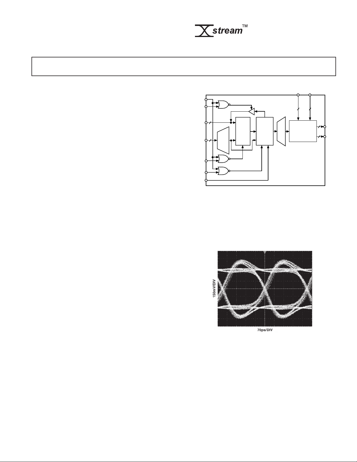
Digital Crosspoint Switch
AD8151*
FUNCTIONAL BLOCK DIAGRAM
INP INN
33
7
D
5
A
OUTPUT
ADDRESS
DECODER
FIRST
RANK
17
7-BIT
LATCH
SECOND
RANK
17
7-BIT
LATCH
DIFFERENTIAL
INPUT
DECODERS
AD8151
33 17
SWITCH
MATRIX
33
17
OUTP
17
OUTN
APPLICATIONS
High-Speed Serial Backplane Routing to OC-48 with FEC
Fiber Optic Network Switching
Fiber Channel
LVDS
PRODUCT DESCRIPTION
AD8151 is a member of the X
stream
line of products and is
a breakthrough in digital switching, offering a large switch array
(33 × 17) on very little power, typically less than 1.5 W. Additionally, it operates at data rates in excess of 3.2 Gb/s per port,
making it suitable for Sonet OC-48 with 8b/10b Forward Error
Correction (FEC). Further, the pricing of the AD8151 makes
it affordable enough to be used for lower data rates as well.
The AD8151’s flexible supply voltages allow the user to operate
with either PECL or ECL data levels and will operate down to
3.3 V for further power reduction. The control interface is CMOS/
TTL compatible (3 V to 5 V).
Its fully differential signal path reduces jitter and crosstalk while
allowing the use of smaller single-ended voltage swings.
The AD8151 is offered in a 184-lead LQFP package that operates
over the extended commercial temperature range of 0°C to 85°C.
*Patent Pending.
X
stream
is a trademark of Analog Devices, Inc.
Figure 1. Eye Pattern, 3.2 Gb/s, PRBS 23
REV. 0
Information furnished by Analog Devices is believed to be accurate and
reliable. However, no responsibility is assumed by Analog Devices for its
use, nor for any infringements of patents or other rights of third parties that
may result from its use. No license is granted by implication or otherwise
under any patent or patent rights of Analog Devices.
One Technology Way, P.O. Box 9106, Norwood, MA 02062-9106, U.S.A.
Tel: 781/329-4700 www.analog.com
Fax: 781/326-8703 © Analog Devices, Inc., 2001

AD8151–SPECIFICATIONS
(@ 25C, VCC = 3.3 V to 5 V, VEE = 0 V, RL = 50 (see TPC 22), I
otherwise noted.)
= 16 mA, unless
OUT
Parameter Conditions Min Typ Max Unit
DYNAMIC PERFORMANCE
Max Data Rate/Channel (NRZ) 2.5 3.2 Gb/s
Channel Jitter Data Rate = 3.2 Gb/s 52 ps p-p
RMS Channel Jitter 8ps
Propagation Delay Input to Output 650 ps
Propagation Delay Match ±50 ±100 ps
Output Rise/Fall Time 20% to 80% 100 ps
INPUT CHARACTERISTICS
Input Voltage Swing Single-Ended 200 1000 mV p-p
Input Bias Current 2 µA
Input Capacitance 2pF
Input V
High VCC – 1.2 V
IN
CC
V
Input VIN Low VCC – 2.4 VCC – 1.4 V
OUTPUT CHARACTERISTICS
Output Voltage Swing Differential (See TPC 22) 800 mV p-p
Output Voltage Range V
– 1.8 V
CC
CC
V
Output Current 5 25 mA
Output Capacitance 2pF
Output V
Output V
High VCC – 1.8 V
OUT
Low V
OUT
CC
V
POWER SUPPLY
Operating Range
PECL, V
ECL, V
V
V
EE
DD
SS
CC
VEE = 0 V 3.0 5.25 V
VCC = 0 V –5.25 –3.0 V
35V
0V
Quiescent Current
V
DD
V
EE
All Outputs Enabled, I
to T
T
MIN
MAX
= 16 mA 425 mA
OUT
2mA
450 mA
All Outputs Disabled 35 mA
THERMAL CHARACTERISTICS
Operating Temperature Range 0 85 °C
θ
JA
LOGIC INPUT CHARACTERISTICS V
Input V
High 1.9 V
IN
= 3 V dc to 5 V dc
DD
30 °C/W
DD
V
Input VIN Low 0 0.9 V
–2–
REV. 0
AD8151
WARNING!
ESD SENSITIVE DEVICE
ABSOLUTE MAXIMUM RATINGS
1
Supply Voltage
V
DD–VEE
V
CC
V
DD
V
SS
V
SS
V
DD
Internal Power Dissipation
. . . . . . . . . . . . . . . . . . . . . . . . . . . . . . . . . . 10.5 V
– VEE . . . . . . . . . . . . . . . . . . . . . . . . . . . . . . . . . . . 5.5 V
– VSS . . . . . . . . . . . . . . . . . . . . . . . . . . . . . . . . . . . 5.5 V
– VEE . . . . . . . . . . . . . . . . . . . . . . . . . . . . . . . . . . . 5.5 V
– VCC . . . . . . . . . . . . . . . . . . . . . . . . . . . . . . . . . . . 5.5 V
– VCC . . . . . . . . . . . . . . . . . . . . . . . . . . . . . . . . . . 5.5 V
2
AD8151 184-Lead Plastic LQFP (ST) . . . . . . . . . . . . 4.2 W
Differential Input Voltage . . . . . . . . . . . . . . . . . . . . . . . . 2.0 V
Storage Temperature Range . . . . . . . . . . . . –65°C to +125°C
Lead Temperature Range (Soldering 10 sec) . . . . . . . . . 300°C
NOTES
1
Stresses above those listed under Absolute Maximum Ratings may cause perma-
nent damage to the device. This is a stress rating only; functional operation of the
device at these or any other conditions above those indicated in the operational
section of this specification is not implied. Exposure to absolute maximum rating
conditions for extended periods may affect device reliability.
2
Specification is for device in free air (TA = 25°C):
184-lead plastic LQFP (ST): θJA = 30°C/W.
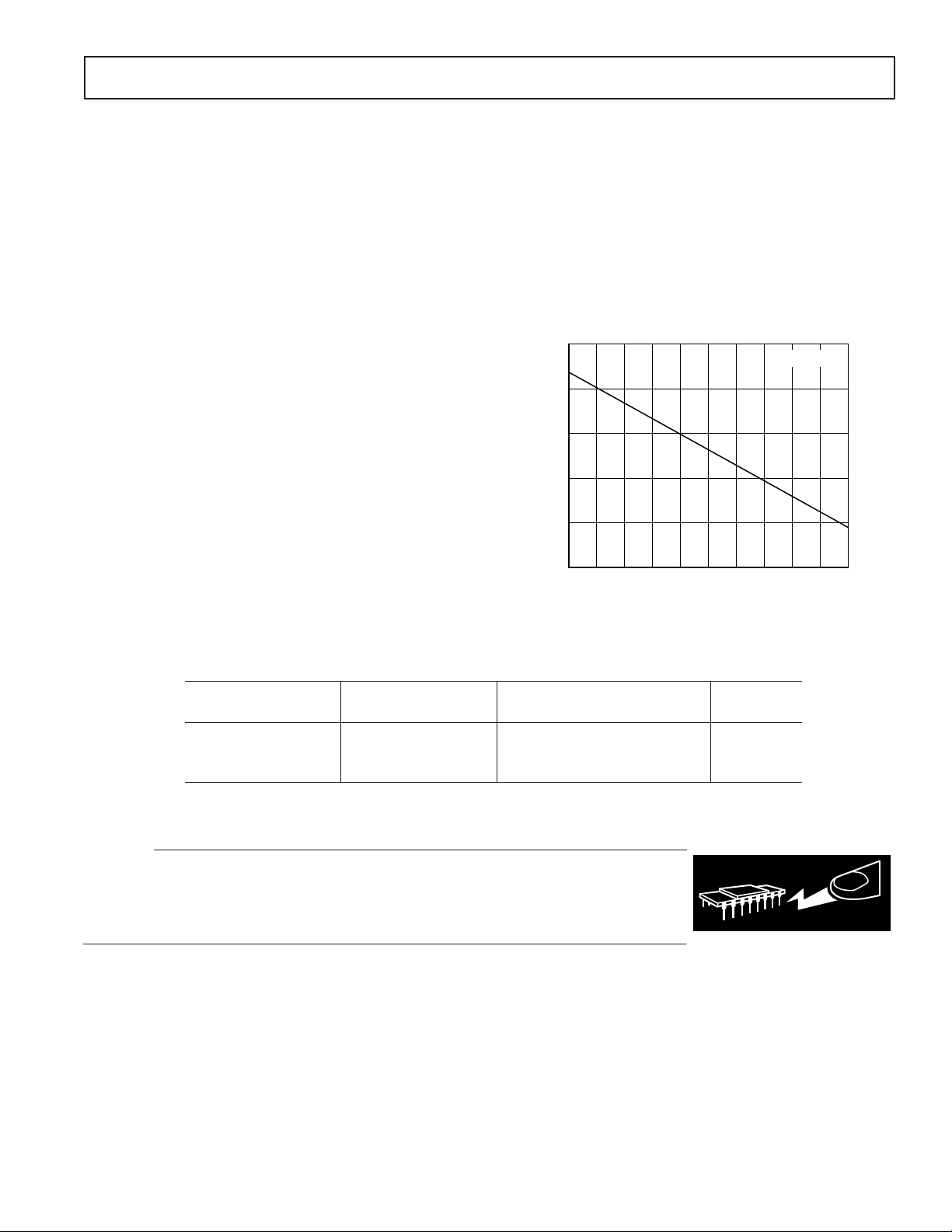
MAXIMUM POWER DISSIPATION
The maximum power that can be safely dissipated by the AD8151
is limited by the associated rise in junction temperature. The
maximum safe junction temperature for plastic encapsulated
devices is determined by the glass transition temperature of
the plastic, approximately 150°C. Temporarily exceeding this
limit may cause a shift in parametric performance due to a change
in the stresses exerted on the die by the package. Exceeding a
junction temperature of 175°C for an extended period can result in
device failure.
To ensure proper operation, it is necessary to observe the maximum power derating curves shown in Figure 2.
6.0
5.0
4.0
3.0
2.0
MAXIMUM POWER DISSIPATION – Watts
1.0
–10 0 10 2030405060708090
AMBIENT TEMPERATURE – C
TJ = 150C
Figure 2. Maximum Power Dissipation vs. Temperature
ORDERING GUIDE
Temperature Package Package
Model Range Description Option
AD8151AST 0°C to 85°C 184-Lead Plastic LQFP ST-184
(20 mm × 20 mm)
AD8151-EVAL Evaluation Board
CAUTION
ESD (electrostatic discharge) sensitive device. Electrostatic charges as high as 4000 V readily
accumulate on the human body and test equipment and can discharge without detection. Although
the AD8151 features proprietary ESD protection circuitry, permanent damage may occur on
devices subjected to high-energy electrostatic discharges. Therefore, proper ESD precautions are
recommended to avoid performance degradation or loss of functionality.
REV. 0
–3–

AD8151
OUT16N
OUT16P
VEEA16
V
IN20P
IN20N
V
IN21P
IN21N
V
IN22P
IN22N
V
IN23P
IN23N
V
IN24P
IN24N
V
IN25P
IN25N
V
IN26P
IN26N
V
IN27P
IN27N
V
IN28P
IN28N
V
IN29P
IN29N
V
IN30P
IN30N
V
IN31P
IN31N
V
IN32P
IN32N
V
V
V
V
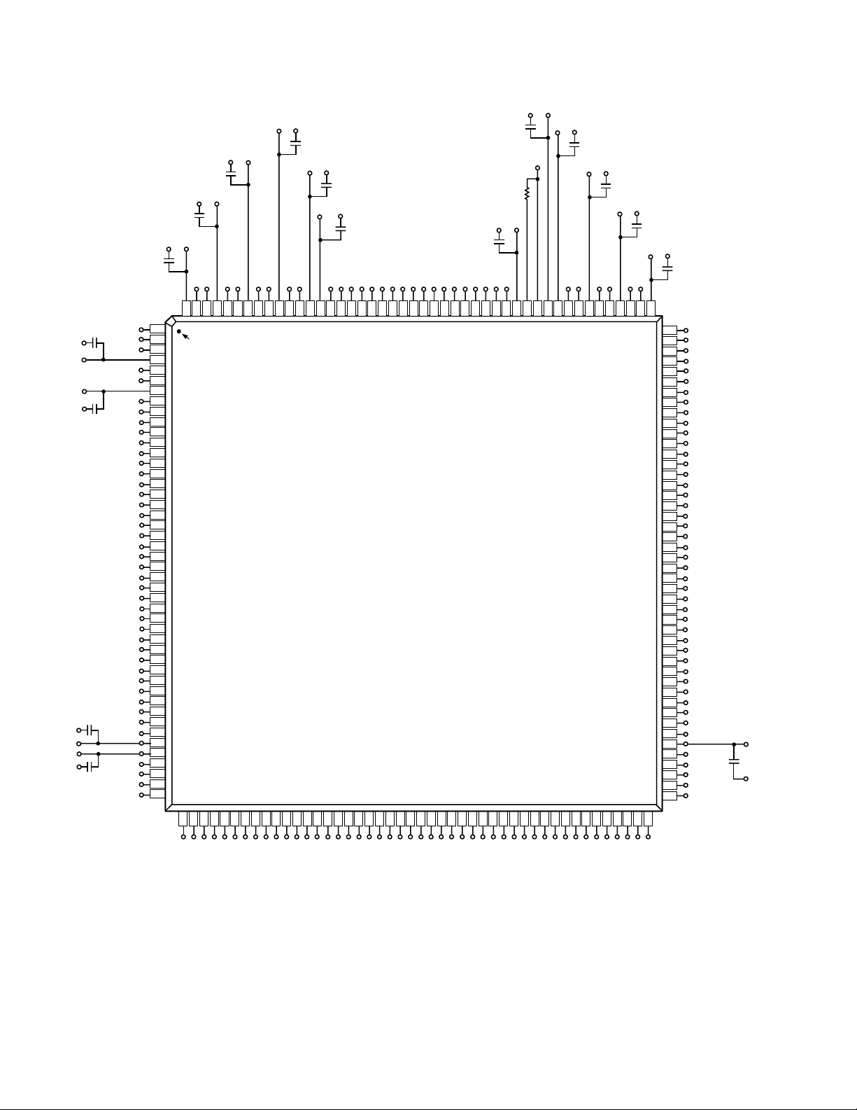
PIN CONFIGURATION
REF
EE
VEEIN19N
IN19P
VEEIN18N
IN18P
VEEIN17N
IN17P
VEEIN16N
IN16P
VEEVCCVDDRESETCSREWEUPDATEA0A1A2A3A4D0D1D2D3D4D5D6
184
183
182
181
180
179
178
177
176
175
174
173
170
169
168
167
166
165
164
AD8151
184L LQFP
TOP VIEW
(Not to Scale)
A10
EE
V
OUT09P
OUT09N
163
160
159
157
156
155
154
OUT06P
OUT06N
A6
EE
V
OUT05N
153
161
A8
EE
V
OUT08P
158
A7
V
OUT07P
OUT07N
EE
162
68
6970717274757677787379808182848586
A9
EE
V
OUT08N
172
171
1
EE
EE
EE
EE
EE
EE
EE
EE
EE
EE
EE
EE
EE
EE
CC
EE
EE
PIN 1
2
IDENTIFIER
3
4
5
6
7
8
9
10
11
12
13
14
15
16
17
18
19
20
21
22
23
24
25
26
27
28
29
30
31
32
33
34
35
36
37
38
39
40
41
42
43
44
45
46
4748495051525354555657
EE
V
A15
EE
V
OUT15P
OUT15N
OUT14P
OUT14N
A14
EE
V
OUT13N
A13
EE
V
OUT13P
OUT12N
596061626364656667
58
A12
A11
EE
EE
V
OUT11P
OUT11N
V
OUT10N
OUT10P
OUT12P
VSSREF
152
151
A5
EE
V
OUT05P
CCVEE
V
V
150
149
A4
V
OUT04P
OUT04N
IN15N
147
148
EE
OUT03N
IN15P
VEEIN14N
146
145
144
87838889909192
A3
EE
V
OUT03P
OUT02N
IN14P
143
OUT02P
VEEIN13N
142
141
A2
EE
V
OUT01N
EE
IN13P
V
140
139
EE
V
OUT01P
138
137
136
135
134
133
132
131
130
129
128
127
126
125
124
123
122
121
120
119
118
117
116
115
114
113
112
111
110
109
108
107
106
105
104
103
102
101
100
99
98
97
96
95
94
93
V
EE
IN12N
IN12P
V
EE
IN11N
IN11P
V
EE
IN10N
IN10P
V
EE
IN09N
IN09P
V
EE
IN08N
IN08P
V
EE
IN07N
IN07P
V
EE
IN06N
IN06P
V
EE
IN05N
IN05P
V
EE
IN04N
IN04P
V
EE
IN03N
IN03P
V
EE
IN02N
IN02P
V
EE
IN01N
IN01P
V
EE
IN00N
IN00P
V
EE
V
CC
VEEA0
OUT00P
OUT00N
VEEA1
V
EE
–4–
REV. 0
PIN FUNCTION DESCRIPTIONS
Pin No. Signal Type Description
1, 4, 7, 10, 13, 16, 19, 22, 25, 28, 31, V
EE
34, 37, 40, 42, 46, 47, 92, 93, 99, 102, Points Labeled V
Power Supply Most Negative PECL Supply (Common with Other
)
EE
105, 108, 111, 114, 117, 120, 123,
126, 129, 132, 135, 138, 139, 142,
145, 148, 172, 175, 178, 181, 184
2 IN20P PECL/ECL High-Speed Input
3 IN20N PECL/ECL High-Speed Input Complement
5 IN21P PECL/ECL High-Speed Input
6 IN21N PECL/ECL High-Speed Input Complement
8 IN22P PECL/ECL High-Speed Input
9 IN22N PECL/ECL High-Speed Input Complement
11 IN23P PECL/ECL High-Speed Input
12 IN23N PECL/ECL High-Speed Input Complement
14 IN24P PECL/ECL High-Speed Input
15 IN24N PECL/ECL High-Speed Input Complement
17 IN25P PECL/ECL High-Speed Input
18 IN25N PECL/ECL High-Speed Input Complement
20 IN26P PECL/ECL High-Speed Input
21 IN26N PECL/ECL High-Speed Input Complement
23 IN27P PECL/ECL High-Speed Input
24 IN27N PECL/ECL High-Speed Input Complement
26 IN28P PECL/ECL High-Speed Input
27 IN28N PECL/ECL High-Speed Input Complement
29 IN29P PECL/ECL High-Speed Input
30 IN29N PECL/ECL High-Speed Input Complement
32 IN30P PECL/ECL High-Speed Input
33 IN30N PECL/ECL High-Speed Input Complement
35 IN31P PECL/ECL High-Speed Input
36 IN31N PECL/ECL High-Speed Input Complement
38 IN32P PECL/ECL High-Speed Input
39 IN32N PECL/ECL High-Speed Input Complement
41, 98, 149, 171 V
CC
Power Supply Most Positive PECL Supply (Common with Other
Points Labeled V
CC
)
43 OUT16N PECL/ECL High-Speed Output Complement
44 OUT16P PECL/ECL High-Speed Output
45 V
A16 Power Supply Most Negative PECL Supply (Unique to This Output)
EE
48 OUT15N PECL/ECL High-Speed Output Complement
49 OUT15P PECL/ECL High-Speed Output
50 V
A15 Power Supply Most Negative PECL Supply (Unique to this Output)
EE
51 OUT14N PECL/ECL High-Speed Output Complement
52 OUT14P PECL/ECL High-Speed Output
53 V
A14 Power Supply Most Negative PECL Supply (Unique to this Output)
EE
54 OUT13N PECL/ECL High-Speed Output Complement
55 OUT13P PECL/ECL High-Speed Output
56 V
A13 Power Supply Most Negative PECL Supply (Unique to this Output)
EE
57 OUT12N PECL/ECL High-Speed Output Complement
58 OUT12P PECL/ECL High-Speed Output
59 V
A12 Power Supply Most Negative PECL Supply (Unique to this Output)
EE
60 OUT11N PECL/ECL High-Speed Output Complement
61 OUT11P PECL/ECL High-Speed Output
AD8151
REV. 0
–5–

AD8151
Pin No. Signal Type Description
62 V
63 OUT10N PECL/ECL High-Speed Output Complement
64 OUT10P PECL/ECL High-Speed Output
65 V
66 OUT09N PECL/ECL High-Speed Output Complement
67 OUT09P PECL/ECL High-Speed Output
68 V
69 OUT08N PECL/ECL High-Speed Output Complement
70 OUT08P PECL/ECL High-Speed Output
71 V
72 OUT07N PECL/ECL High-Speed Output Complement
73 OUT07P PECL/ECL High-Speed Output
74 V
75 OUT06N PECL/ECL High-Speed Output Complement
76 OUT06P PECL/ECL High-Speed Output
77 V
78 OUT05N PECL/ECL High-Speed Output Complement
79 OUT05P PECL/ECL High-Speed Output
80 V
81 OUT04N PECL/ECL High-Speed Output Complement
82 OUT04P PECL/ECL High-Speed Output
83 V
84 OUT03N PECL/ECL High-Speed Output Complement
85 OUT03P PECL/ECL High-Speed Output
86 V
87 OUT02N PECL/ECL High-Speed Output Complement
88 OUT02P PECL/ECL High-Speed Output
89 V
90 OUT01N PECL/ECL High-Speed Output Complement
91 OUT01P PECL/ECL High-Speed Output
94 V
95 OUT00N PECL/ECL High-Speed Output Complement
96 OUT00P PECL/ECL High-Speed Output
97 V
100 IN00P PECL/ECL High-Speed Input
101 IN00N PECL/ECL High-Speed Input Complement
103 IN01P PECL/ECL High-Speed Input
104 IN01N PECL/ECL High-Speed Input Complement
106 IN02P PECL/ECL High-Speed Input
107 IN02N PECL/ECL High-Speed Input Complement
109 IN03P PECL/ECL High-Speed Input
110 IN03N PECL/ECL High-Speed Input Complement
112 IN04P PECL/ECL High-Speed Input
113 IN04N PECL/ECL High-Speed Input Complement
115 IN05P PECL/ECL High-Speed Input
116 IN05N PECL/ECL High-Speed Input Complement
118 IN06P PECL/ECL High-Speed Input
119 IN06N PECL/ECL High-Speed Input Complement
121 IN07P PECL/ECL High-Speed Input
122 IN07N PECL/ECL High-Speed Input Complement
A11 Power Supply Most Negative PECL Supply (Unique to this Output)
EE
A10 Power Supply Most Negative PECL Supply (Unique to this Output)
EE
A9 Power Supply Most Negative PECL Supply (Unique to this Output)
EE
A8 Power Supply Most Negative PECL Supply (Unique to this Output)
EE
A7 Power Supply Most Negative PECL Supply (Unique to this Output)
EE
A6 Power Supply Most Negative PECL Supply (Unique to this Output)
EE
A5 Power Supply Most Negative PECL Supply (Unique to this Output)
EE
A4 Power Supply Most Negative PECL Supply (Unique to this Output)
EE
A3 Power Supply Most Negative PECL Supply (Unique to this Output)
EE
A2 Power Supply Most Negative PECL Supply (Unique to this Output)
EE
A1 Power Supply Most Negative PECL Supply (Unique to this Output)
EE
A0 Power Supply Most Negative PECL Supply (Unique to this Output)
EE
–6–
REV. 0
AD8151
Pin No. Signal Type Description
124 IN08P PECL/ECL High-Speed Input
125 IN08N PECL/ECL High-Speed Input Complement
127 IN09P PECL/ECL High-Speed Input
128 IN09N PECL/ECL High-Speed Input Complement
130 IN10P PECL/ECL High-Speed Input
131 IN10N PECL/ECL High-Speed Input Complement
133 IN11P PECL/ECL High-Speed Input
134 IN11N PECL/ECL High-Speed Input Complement
136 IN12P PECL/ECL High-Speed Input
137 IN12N PECL/ECL High-Speed Input Complement
140 IN13P PECL/ECL High-Speed Input
141 IN13N PECL/ECL High-Speed Input Complement
143 IN14P PECL/ECL High-Speed Input
144 IN14N PECL/ECL High-Speed Input Complement
146 IN15P PECL/ECL High-Speed Input
147 IN15N PECL/ECL High-Speed Input Complement
150 V
151 REF R-Program Connection Point for Output Logic Pull-Down
152 V
153 D6 TTL Enable/Disable Output
154 D5 TTL (32) MSB Input Select
155 D4 TTL (16)
156 D3 TTL (8)
157 D2 TTL (4)
158 D1 TTL (2)
159 D0 TTL (1) LSB Input Select
160 A4 TTL (16) MSB Output Select
161 A3 TTL (8)
162 A2 TTL (4)
163 A1 TTL (2)
164 A0 TTL (1) LSB Output Select
165 UPDATE TTL Second Rank Program
166 WE TTL First Rank Program
167 RE TTL Enable Readback
168 CS TTL Enable Chip to Accept Programming
169 RESET TTL Disable All Outputs (Hi-Z)
170 V
173 IN16P PECL/ECL High-Speed Input
174 IN16N PECL/ECL High-Speed Input Complement
176 IN17P PECL/ECL High-Speed Input
177 IN17N PECL/ECL High-Speed Input Complement
179 IN18P PECL/ECL High-Speed Input
180 IN18N PECL/ECL High-Speed Input Complement
182 IN19P PECL/ECL High-Speed Input
183 IN19N PECL/ECL High-Speed Input Complement
REF R-Program Connection Point for Output Logic Pull-Down
EE
Programming Resistor (Must be Connected to V
Programming Resistor
SS
DD
Power Supply Most Negative Control Logic Supply
Power Supply Most Positive Control Logic Supply
EE
)
REV. 0
–7–
AD8151
–Typical Performance Characteristics
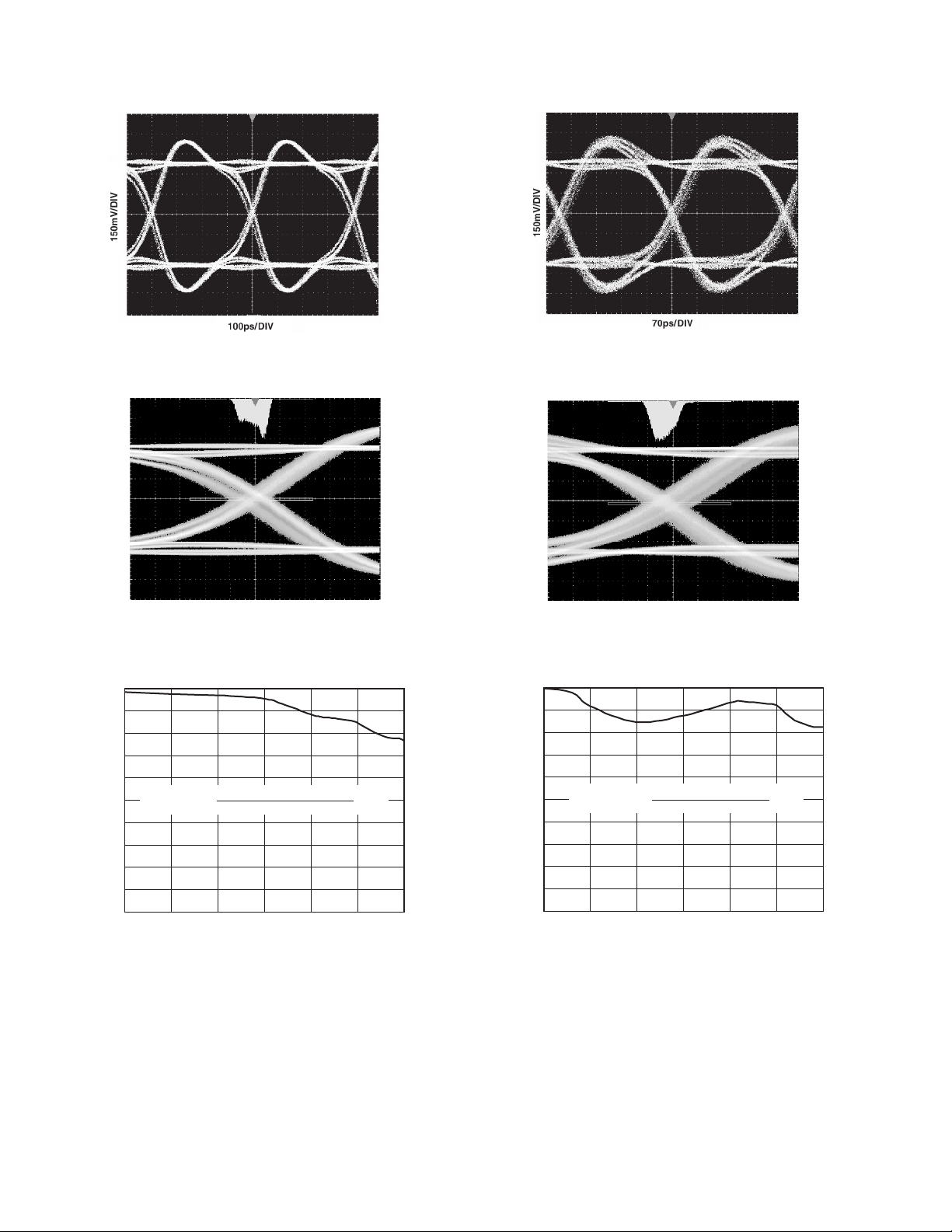
TPC 1. Eye Pattern 2.5 Gb/s, PRBS 23
p-p = 43ps
STD DEV = 8ps
150mV/DIV
20ps/DIV
TPC 2. Jitter @ 2.5 Gb/s, PRBS 23
100
90
80
70
60
50
40
EYE WIDTH – %
30
20
10
0
% EYE WIDTH =
1.0 1.5 2.0 2.5 3.0 3.5
0.5
(CLOCK PERIOD – JITTER p-p)
CLOCK PERIOD
DATA RATE – Gb/s
TPC 3. Eye Width vs. Data Rate, PRBS 23
100
TPC 4. Eye Pattern 3.2 Gb/s, PRBS 23
p-p = 53ps
STD DEV = 8ps
150mV/DIV
20ps/DIV
TPC 5. Jitter @ 3.2 Gb/s, PRBS 23
100
90
80
70
60
% EYE HEIGHT =
50
40
EYE HEIGHT – %
30
20
10
0
1.0 1.5 2.0 2.5 3.0 3.5
0.5
@ DATA RATE)
(V
OUT
V
@ 0.5Gb/s
OUT
DATA RATE – Gb/s
100
TPC 6. Eye Height vs. Data Rate, PRBS 23
–8–
REV. 0
AD8151
100
90
80
70
60
50
40
JITTER – ps
30
20
10
STANDARD DEVIATION
0
1.0
PEAK-PEAK
JITTER
1.5 2.0 2.5 3.0 3.5
DATA RATE – Gb/s
TPC 7. Jitter vs. Data Rate, PRBS 23
150mV/DIV
p-p = 38ps
STD DEV = 7.7ps
100
90
80
70
60
50
JITTER – ps
40
30
20
10
0
3.2Gb/s STD DEV
0 102030405060708090
3.2Gb/s JITTER
2.5Gb/s JITTER
2.5Gb/s STD DEV
TEMPERATURE – C
TPC 10. Jitter vs. Temperature, PRBS 23
150mV/DIV
100ps/DIV
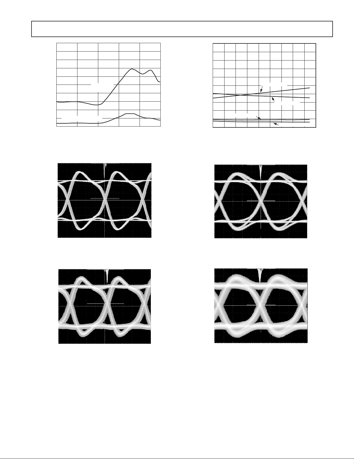
TPC 8. Crosstalk, 2.5 Gb/s, PRBS 23, Attack Signal is OFF
p-p = 70ps
STD DEV = 8ps
150mV/DIV
100ps/DIV
TPC 9. Crosstalk, 2.5 Gb/s, PRBS 23, Attack Signal is ON
p-p = 32ps
STD DEV = 4.7ps
75ps/DIV
TPC 11. Crosstalk, 3.2 Gb/s, PRBS 23, Attack Signal is OFF
150mV/DIV
p-p = 70ps
STD DEV = 9ps
75ps/DIV
TPC 12. Crosstalk, 3.2 Gb/s, PRBS 23, Attack Signal is ON
REV. 0
–9–
AD8151
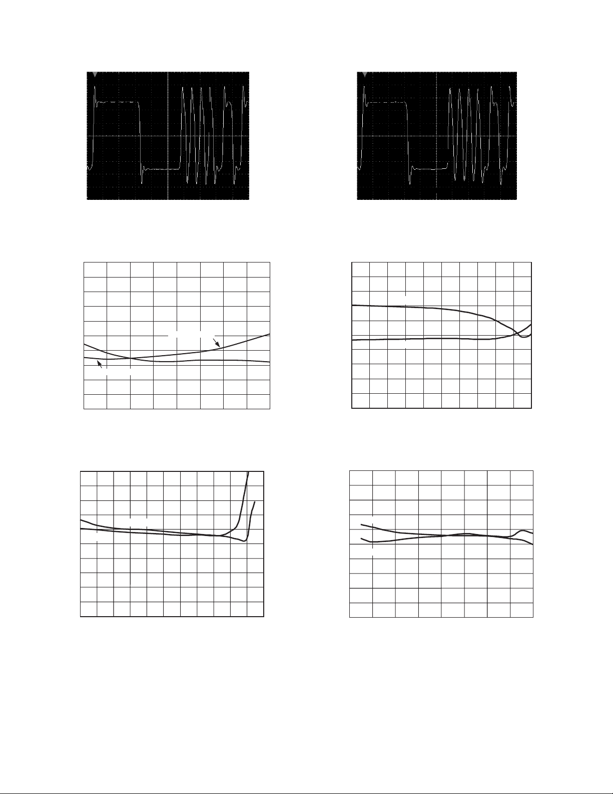
150mV/DIV
1.4ns/DIV
TPC 13. Response, 2.5 Gb/s, 32-Bit Pattern
1111 1111 0000 0000 0101 0101 0011 0011
100
90
80
70
60
50
40
P-P JITTER – ps
30
3.2Gb/s JITTER
20
10
0
0.2 0.3 0.5 0.6 0.7 0.8 0.9 10.4
2.5Gb/s JITTER
INPUT AMPLITUDE – V
TPC 14. Jitter vs. Single-Ended Input Amplitude, PRBS 23
150mV/DIV
1.1ns/DIV
TPC 16. Response, 3.2 Gb/s, 32-Bit Pattern
1111 1111 0000 0000 0101 0101 0011 0011
100
90
80
70
60
50
40
P-P JITTER – ps
30
20
10
0
–5.0 –4.8 –4.6 –4.4 –4.2 –4.0 –3.8 –3.6 –3.4 –3.2 –3.0
3.2Gb/s
2.5Gb/s
– V
V
EE
TPC 17. Jitter vs. Supply, PRBS 23
100
90
80
70
60
3.2Gb/s
50
40
P-P JITTER – ps
30
20
10
0
–1.6 –1.4 –1.2 –1.0 –0.8 –0.6 –0.4 –0.2 0 0.2 0.4 0.6
2.5Gb/s
VIH – V
TPC 15. Jitter vs. VIH, PRBS 23
100
90
80
70
3.2Gb/s
60
50
2.5Gb/s
40
P-P JITTER – ps
30
20
10
0
–1.4 –1.2 –1.0 –0.8 –0.6 –0.4 –0.2 0 0.2
V
– V
OH
TPC 18. Jitter vs. VOH, PRBS 23, Output Amplitude = 0.4 V
Single-Ended
–10–
REV. 0
AD8151
100
90
80
70
60
50
40
FREQUENCY
30
20
10
0
550 570 590 610 630 650 670 690 710 730
PROPAGATION DELAY – ps
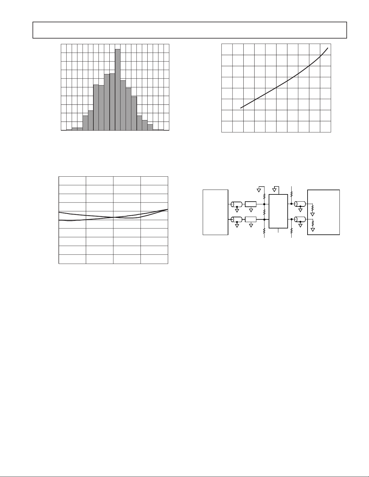
TPC 19. Variation in Channel-to-Channel Delay,
All 561 Points
100
90
80
70
2.5Gb/s
60
50
3.2Gb/s
40
P-P JITTER – ps
30
20
10
0
5
10 15 20 25
OUTPUT CURRENT – mA
TPC 20. Jitter vs. I
, PRBS 23
OUT
200
150
100
50
0
–50
–100
PROPAGATION DELAY – ps
–150
–200
–100 –80 –60 –40 –20 0 20 40 60 80 100
NORMALIZED TEMPERATURE – C
TPC 21. Propagation Delay, Normalized at 25°C vs.
Temperature
V
V
TT
CC
49.9
P
N
V
49.9
EE
V
TT
HIGH-SPEED
SAMPLING
OSCILLOSCOPE
50
50
PRBS
GENERATOR
DATA OUT
DATA OUT
V
CC
1.65k
–6dB
–6dB
1.65k
V
= 0V, VEE = –3.3V, VTT = –1.6V, VDD = 5V, VSS = 0V
CC
= 1.54k, I
R
SET
VIN = 0.8V p-p EXCEPT AS NOTED
OUT
AD8151
P
IN OUT
105
N
V
EE
= 16mA, VOH = –0.8V, VOL = –1.2V
TPC 22. Test Circuit
REV. 0
–11–
AD8151
Control Interface Truth Tables
The following are truth tables for the control interface.
Table I. Basic Control Functions
Control Pins
RESET CS WE RE UPDATE Function
0 X X X X Global Reset. Reset all second rank enable bits to zero (disable all outputs).
1 1 X X X Control Disable. Ignore all logic (but the signal matrix still functions as
programmed). D[6:0] are high-impedance.
1 0 0 X X Single Output Preprogram. Write input configuration data from data bus D[6:0].
into first rank of latches for the output selected by the output address bus A[4:0].
1 0 X 0 X Single Output Readback. Readback input configuration data from second rank of latches
onto data bus D[6:0] for the single output selected by the output address bus A[4:0].
1 0 X X 0 Global Update. Copy input configuration data from all 17 first rank latches into second
rank of latches, updating signal matrix connections for all outputs.
1 0 0 1 0 Transparent Write and Update. It is possible to write data directly onto rank two. This
simplifies logic when synchronous signal matrix updating is not necessary.
Table II. Address/Data Examples
Output Address Pins Enable Input Address Pins
MSB–LSB Bit MSB–LSB
A4 A3 A2 A1 A0 D6/E D5 D4 D3 D2 D1 D0 Function
00000X 000000Lower Address/Data Range. Connect Output #00
(A[4:0] = 00000) to Input #00 (D[5:0] = 000000).
10000X 100000Upper Address/Data Range. Connect Output #16
(A[4:0] = 10000) to Input #32 (D[5:0] = 100000).
<Binary Output Number*> 1 <Binary Input Number> Enable Output. Connect Selected Output (A[4:0] = 0
to 16) to Designated Input (D[5:0] = 0 to 32) and
Enable Output (D6 = 1).
<Binary Output Number*>0 XXXXXXDisable Output. Disable Specified Output (D6 = 0).
10001X <Binary Input Number> Broadcast Connection. Connect all 17 outputs to
same designated input and set all 17 enable bits to
the value of D6. Readback is not possible with the
broadcast address.
10010X 100001Reserved. Any address or data code greater or equal
to these are reserved for future expansion or factory
testing.
*The binary output number may also be the broadcast connection designator, 10001.
–12–
REV. 0
AD8151
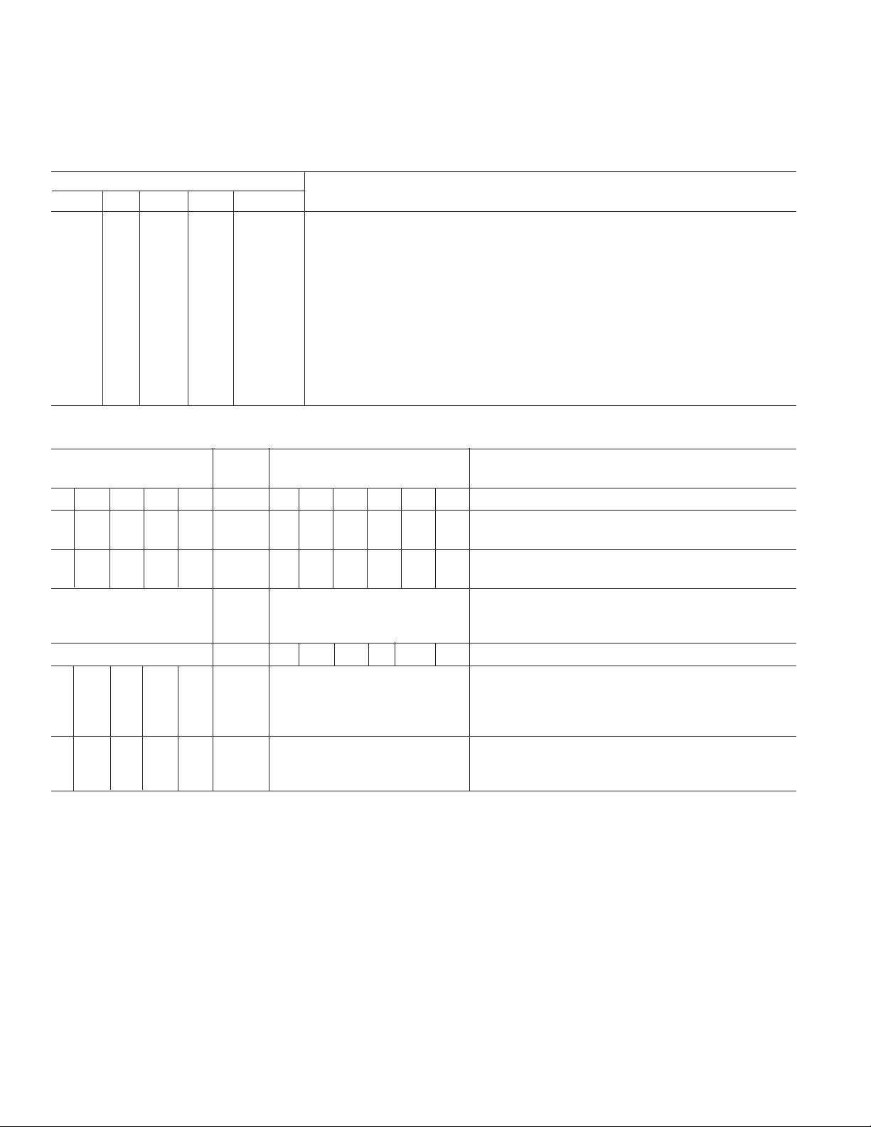
Control Interface Timing Diagrams
CS INPUT
WE INPUT
A[4:0] INPUTS
D[6:0] INPUTS
t
CSW
t
ASW
t
WP
t
DSW
Figure 3. First Rank Write Cycle
Table III. First Rank Write Cycle
Symbol Parameter Conditions Min Typ Max Unit
t
CSW
t
ASW
t
DSW
t
CHW
t
AHW
t
DHW
t
WP
Setup Time Chip Select to Write Enable TA = 25°C0 ns
Address to Write Enable VDD = 5 V 0 ns
Data to Write Enable VCC = 3.3 V 15 ns
Hold Time Chip Select from Write Enable 0 ns
Address from Write Enable 0 ns
Data from Write Enable 0 ns
Width of Write Enable Pulse 15 ns
t
AHW
t
DHW
t
CHW
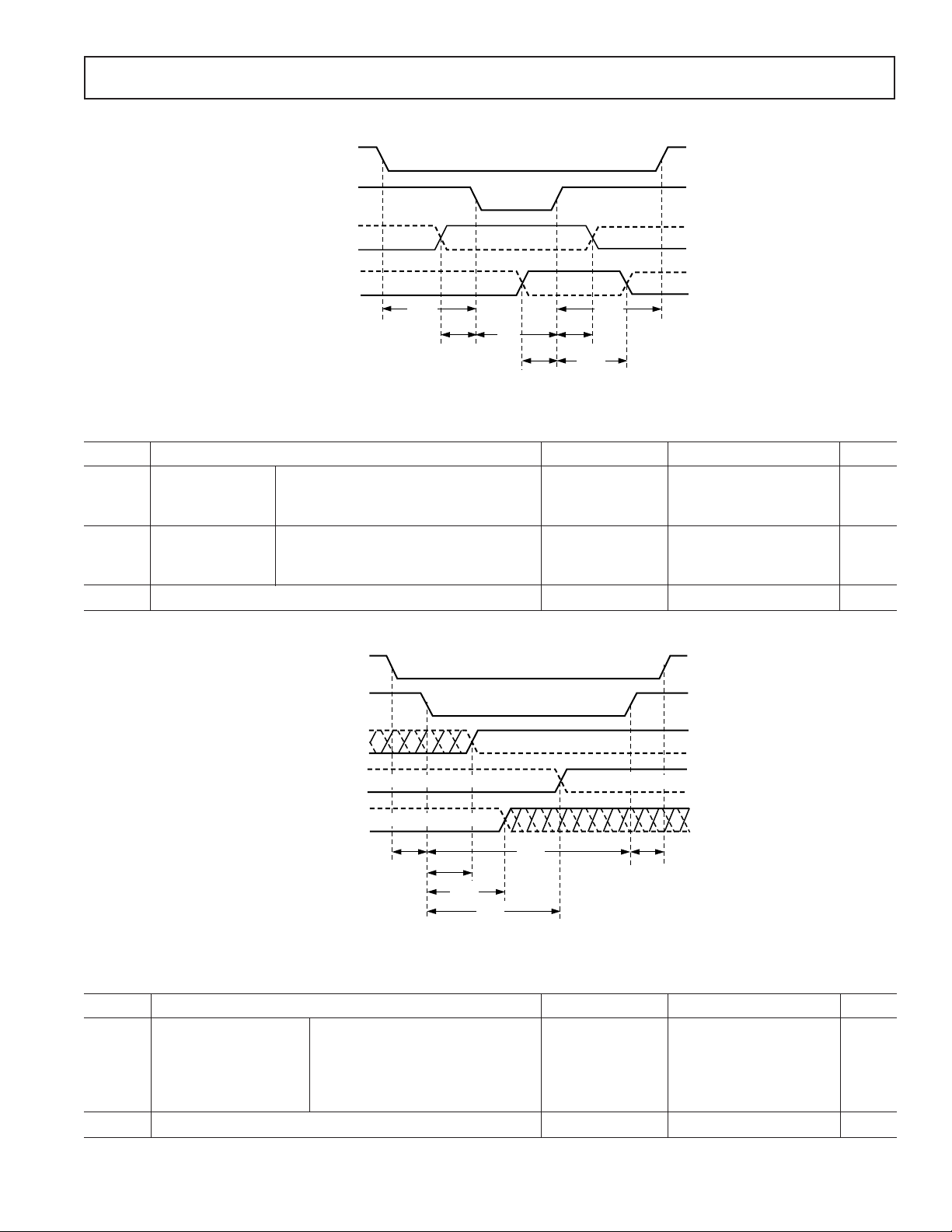
CS INPUT
UPDATE INPUT
ENABLING
OUT[0:16][N:P]
OUTPUTS
TOGGLE
OUT[0:16][N:P]
OUTPUTS
DISABLING
OUT[0:16][N:P]
OUTPUTS
PREVIOUS RANK 2 DATA
DATA FROM RANK 2
t
CSU
t
UOE
DATA FROM RANK 1
t
UOD
t
UOT
DATA FROM RANK 1
t
t
UW
CHU
Figure 4. Second Rank Update Cycle
Table IV. Second Rank Update Cycle
Symbol Parameter Conditions Min Typ Max Unit
t
CSU
t
CHU
t
UOE
t
UOT
t
UOD
t
UW
Setup Time Chip Select to Update TA = 25°C0 ns
Hold Time Chip Select from Update VDD = 5 V 0 ns
Output Enable Times Update to Output Enable VCC = 3.3 V 25 40 ns
Output Toggle Times Update to Output Reprogram 25 40 ns
Output Disable Times Update to Output Disabled 25 30 ns
Width of Update Pulse 15 ns
REV. 0
–13–
AD8151
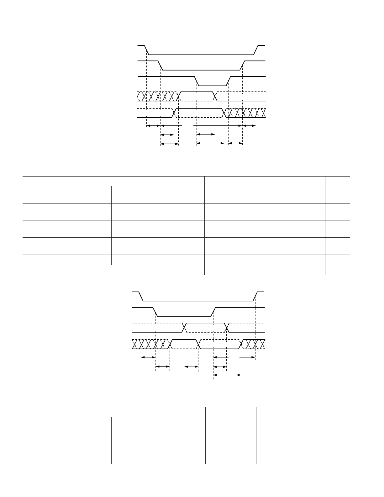
CS INPUT
UPDATE INPUT
WE INPUT
ENABLING
OUT[0:16][N:P]
OUTPUTS
DISABLING
OUT[0:16][N:P]
OUTPUTS
INPUT {DATA 0}
t
CSU
t
Figure 5. First Rank Write Cycle and Second Rank Update Cycle
Table V. First Rank Write Cycle and Second Rank Update Cycle
Symbol Parameter Conditions Min Typ Max Unit
t
CSU
t
CHU
t
UOE
t
WOE
t
UOT
t
WOT
t
UOD
t
WOD
t
WHU
t
UW
*Not Shown.
Setup Time Chip Select to Update TA = 25°C0 ns
Hold Time Chip Select from Update VDD = 5 V 0 ns
Output Enable Times Update to Output Enable VCC = 3.3 V 25 40 ns
* Write Enable to Output Enable 25 40 ns
Output Toggle Times Update to Output Reprogram 25 30 ns
Write Enable to Output Reprogram 25 30 ns
* Output Disable Times Update to Output Disabled 25 30 ns
Write Enable to Output Disabled 25 30 ns
Setup Time Write Enable to Update 10 ns
Width of Update Pulse 15 ns
UOT
t
UOE
INPUT {DATA 1}
INPUT {DATA 1}
t
UW
t
WOT
t
WOD
INPUT {DATA 2}
t
CHU
t
WHU
CS INPUT
RE INPUT
A[4:0]
INPUTS
D[6:0]
OUTPUTS
ADDR 1 ADDR 2
DATA
{ADDR1}
t
CSR
t
RDE
t
AA
DATA {ADDR2}
t
RHA
t
RDD
t
CHR
Figure 6. Second Rank Readback Cycle
Table VI. Second Rank Readback Cycle
Symbol Parameter Conditions Min Typ Max Unit
t
CSR
t
CHR
t
RHA
t
RDE
t
AA
t
RDD
Setup Time Chip Select to Read Enable TA = 25°C0 ns
Hold Time Chip Select from Read Enable VDD = 5 V 0 ns
Address from Read Enable VCC = 3.3 V 5 ns
Enable Time Data from Read Enable 10 kΩ 15 ns
Access Time Data from Address 20 pF on D[6:0] 15 ns
Release Time Data from Read Enable Bus 15 30 ns
–14–
REV. 0
AD8151
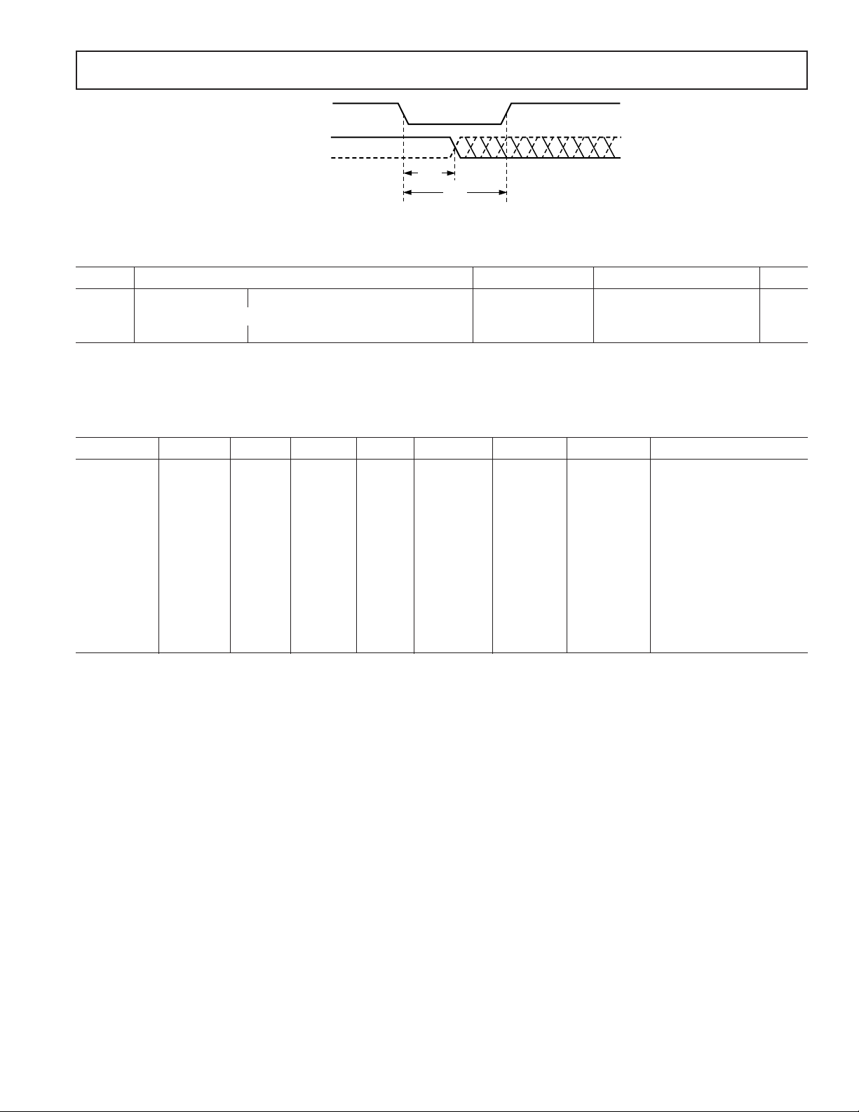
RESET INPUT
DISABLING
OUT[0:16][N:P]
OUTPUTS
t
TOD
t
TW
Figure 7. Asynchronous Reset
Table VII. Asynchronous Reset
Symbol Parameter Conditions Min Typ Max Unit
t
TOD
t
TW
Control Interface Programming Example
The following conservative pattern connects all outputs to input number 7, except output 16 which is connected to input number 32.
The vector clock period, T
Vector No. RESET CS WE RE UPDATE A[4:0] D[6:0] Comments
0 0 1 1 1 1 xxxxx xxxxxxx Disable All Outputs
1 1 1 1 1 1 xxxxx xxxxxxx
2 1 0 1 1 1 10001 1000111 All Outputs to Input #07
3 1 0 0 1 1 10001 1000111 Write to First Rank
4 1 0 1 1 1 10001 1000111
5 1 0 1 1 1 10000 1100000 Output #16 to Input #32
6 1 0 0 1 1 10000 1100000 Write to First Rank
7 1 0 1 1 1 10000 1100000
8 1 0 1 1 0 xxxxx xxxxxxx Transfer to Second Rank
9 1 0 1 1 1 xxxxx xxxxxxx
10 1 1 1 1 1 xxxxx xxxxxxx Disable Interface
Disable Time Output Disable from Reset TA = 25°C2530ns
Width of Reset Pulse VDD = 5 V 15 ns
VCC = 3.3 V
is 15 ns. It is possible to accelerate the execution of this pattern by deleting vectors 1, 4, 7, and 9.
0
Table VIII. Basic Test Pattern
REV. 0
–15–
AD8151
D[0:6]
WE
7
7
7
7
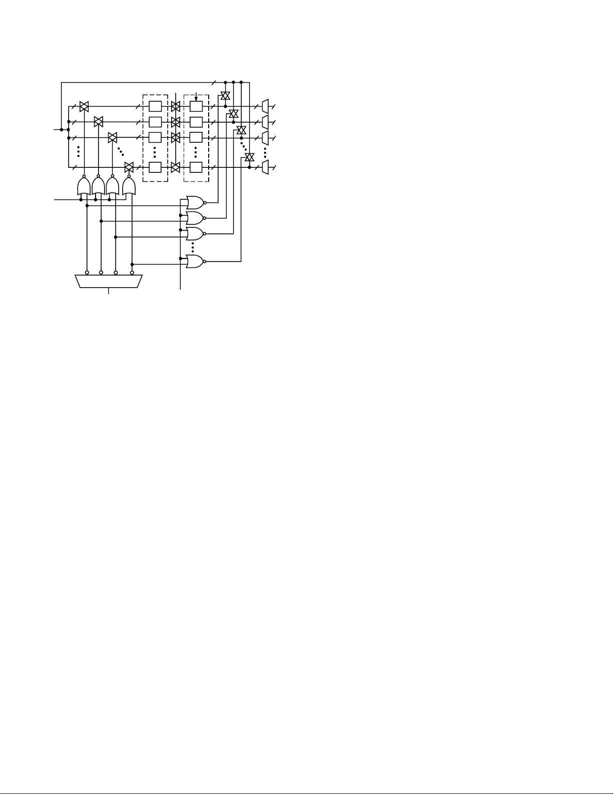
1 OF 17 DECODERS
A[0:4]
UPDATE
7
0
7
1
7
2
7
16
RANK 1
17 ROWS OF 7-BIT
LATCHES
RE
RESET
0
1
2
16
RANK 2
7
7
7
7
7
TO 1733
SWITCH
MATRIX
33
7
33
7
33
7
33
7
1 OF 33
DECODERS
Figure 8. Control Interface (Simplified Schematic)
AD8151 CONTROL INTERFACE
The AD8151 control interface receives and stores the desired
connection matrix for the 33 input and 17 output signal pairs.
The interface consists of 17 rows of double-rank 7-bit latches,
one row for each output. The 7-bit data word stored in each
of these latches indicates to which (if any) of the 33 inputs the
output will be connected.
One output at a time can be preprogrammed by addressing the
output and writing the desired connection data into the first
rank of latches. This process can be repeated until each of the
desired output changes has been preprogrammed. All output
connections can then be programmed at once by passing the
data from the first rank of latches into the second rank. The
output connections always reflect the data programmed into
the second rank of latches, and do not change until the first rank
of data is passed into the second rank.
If necessary for system verification, the data in the second rank
of latches can be read back from the control interface.
At any time, a reset pulse can be applied to the control interface
to globally reset the appropriate second rank data bits, disabling
all 17 signal output pairs. This feature can be used to avoid
output bus contention on system start-up. The contents of the
first rank remain unchanged.
The control interface pins are connected via logic-level translators. These translators allow programming and readback of the
control interface using logic levels different from those in the
signal matrix.
In order to facilitate multiple chip address decoding, there is a
chip-select pin. All logic signals except the reset pulse are ignored
unless the chip select pin is active. The chip select pin disables
only the control logic interface, and does not change the operation of the signal matrix. The chip select pin does not power
down any of the latches, so any data programmed in the latches
is preserved.
All control pins are level-sensitive, not edge-triggered.
CONTROL PIN DESCRIPTION
A[4:0] Inputs
Output address pins. The binary encoded address applied to
these five input pins determines which one of the seventeen
outputs is being programmed (or being read back). The most
significant bit is A4.
D[6:0] Inputs/Outputs
Input configuration data pins. In write mode, the binary encoded
data applied to pins D[6:0] determine which one of 33 inputs is
to be connected to the output specified with the A[4:0] pins.
The most significant bit is D5, and the least significant bit is
D0. Bit D6 is the enable bit, setting the specified output signal pair to an enabled state if D6 is logic HIGH, or disabled
to a high-impedance state if D6 is logic LOW.
In readback mode, pins D[6:0] are low-impedance outputs indicating the data word stored in the second rank for the output
specified with the A[4:0] pins. The readback drivers were designed
to drive high impedances only, so external drivers connected
to the D[6:0] should be disabled during readback mode.
WE Input
First Rank Write Enable. Forcing this pin to logic LOW allows
the data on pins D[6:0] to be stored in the first rank latch for
the output specified by pins A[4:0]. The WE pin must be returned
to a logic HIGH state after a write cycle to avoid overwriting
the first rank data.
UPDATE Input
Second Rank Write Enable. Forcing this pin to logic LOW allows
the data stored in all 17 first rank latches to be transferred to the
second rank latches. The signal connection matrix will be reprogrammed when the second rank data is changed. This is a global
pin, transferring all 17 rows of data at once. It is not necessary
to program the address pins. It should be noted that after initial
power-up of the device, the first rank data is undefined. It may
be desirable to preprogram all seventeen outputs before performing
the first update cycle.
RE Input
Second Rank Read-Enable. Forcing this pin to logic LOW enables
the output drivers on the bidirectional D[6:0] pins, entering the
readback mode of operation. By selecting an output address with
the A[4:0] pins and forcing RE to logic LOW, the 7-bit data
stored in the second rank latch for that output address will be
written to D[6:0] pins. Data should not be written to the D[6:0]
pins externally while in readback mode. The RE and WE pins
are not exclusive, and may be used at the same time, but data
should not be written to the D[6:0] pins from external sources
while in readback mode.
CS Input
Chip-Select. This pin must be forced to logic LOW in order
to program or receive data from the logic interface, with the
exception of the RESET pin, described below. This pin has
no effect on the signal pairs and does not alter any of the stored
control data.
RESET Input
Global Output Disable Pin. Forcing the RESET pin to logic
LOW will reset the enable bit, D6, in all 17 second rank
latches, regardless of the state of any other pins. This has the
effect of immediately disabling the 17 output signal pairs in the
–16–
REV. 0
AD8151
V
CC
INxxP
INxxN
Z
O
Z
O
Z
O
Z
O
ECL SOURCE
V
TT
= VCC – 2V
(a)
V
CC
INxxP
INxxN
Z
O
Z
O
R2 R2
R1
R1
V
EE
ECL SOURCE
V
CC
– 2V
(b)
V
CC
INxxP
INxxN
Z
O
R
L
Z
O
2Z
O
R
L
V
EE
ECL SOURCE
(c)
matrix. It is useful to momentarily hold RESET at a logic LOW
state when powering up the AD8151 in a system that has multiple output signal pairs connected together. Failure to do this
may result in several signal outputs contending after power-up.
The reset pin is not gated by the state of the chip-select pin, CS.
It should be noted that the RESET pin does not program the
first rank, which will contain undefined data after power-up.
CONTROL INTERFACE TRANSLATORS
The AD8151 control interface has two supply pins, VDD and
. The potential between the positive logic supply VDD and
V
SS
the negative logic supply V
must be at least 3 V and no more
SS
than 5 V. Regardless of supply, the logic threshold is approximately 1.6 V above V
, allowing the interface to be used with
SS
most CMOS and TTL logic drivers.
The signal matrix supplies, V
dent of the voltage on V
(V
) ≤ 10 V. These constraints will allow operation of
DD–VEE
DD
and VEE, can be set indepen-
CC
and VSS, with the constraints that
the control interface on 3 V or 5 V while the signal matrix is
operated on +3.3 V or +5 V PECL, or –3.3 V or –5 V ECL.
CIRCUIT DESCRIPTION
The AD8151 is a high-speed 33 × 17 differential crosspoint switch
designed for data rates up to 3.2 Gb/s per channel. The AD8151
supports PECL-compatible input and output levels when operated
from a 5 V supply (V
levels when operated from a –5 V supply (V
= 5 V, VEE = GND) or ECL-compatible
CC
= GND, VEE =
CC
–5 V). To save power, the AD8151 can run from a +3.3 V supply
to interface with low-voltage PECL circuits or a –3.3 V supply
to interface with low-voltage ECL circuits. The AD8151 utilizes
differential current mode outputs with individual disable control,
which facilitates busing together the outputs of multiple AD8151s
to assemble larger switch arrays. This feature also reduces system crosstalk and can greatly reduce power dissipation in a large
switch array. A single external resistor programs the current for
all enabled output stages, allowing for user control over output
levels with different output termination schemes and transmission line characteristic impedances.
High-Speed Data Inputs (INxxP, INxxN)
The AD8151 has 33 pairs of differential voltage-mode inputs.
The common-mode input range extends from the positive supply voltage (V
levels (V
) down to include standard ECL or PECL input
CC
– 2 V). The minimum differential input voltage is
CC
200 mV. Unused inputs may be connected directly to any level
within the allowed common-mode input range. A simplified
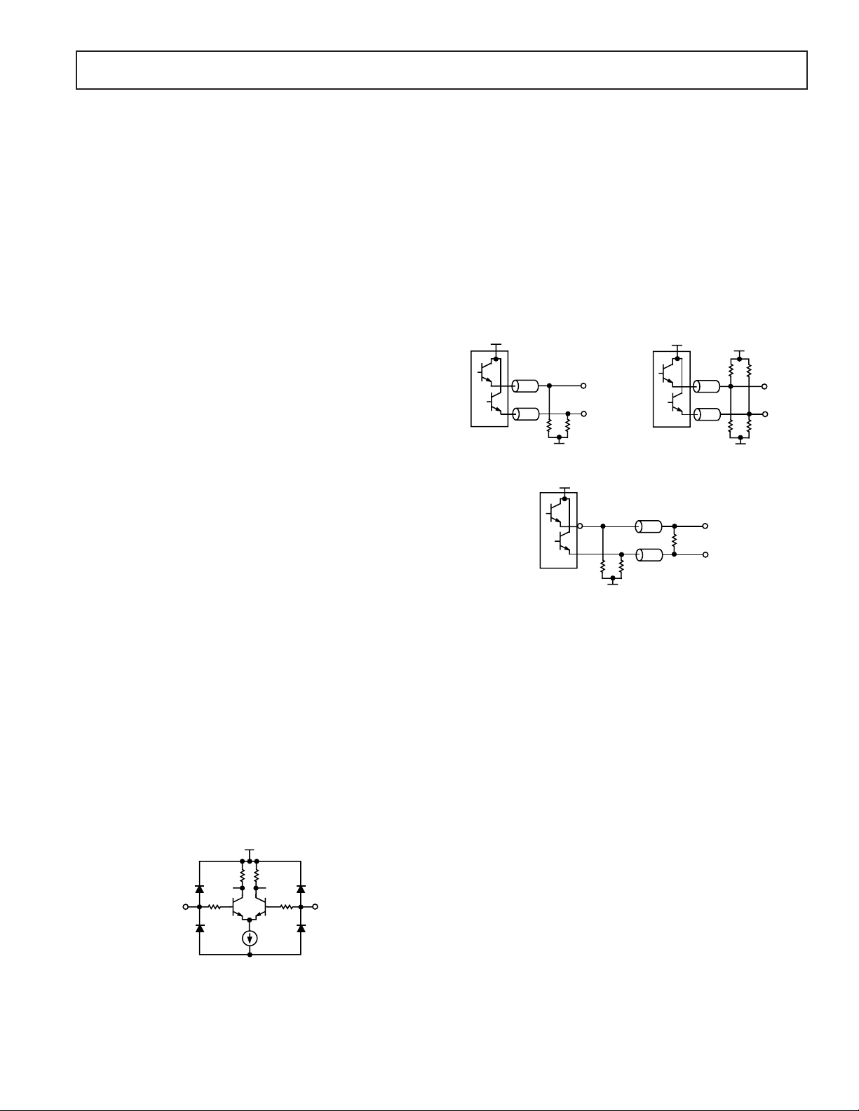
schematic of the input circuit is shown in Figure 9.
INxxP
Figure 9. Simplified Input Circuit
V
CC
V
EE
INxxN
In order to maintain signal fidelity at the high data rates supported
by the AD8151, the input transmission lines should be terminated
as close to the input pins as possible. The preferred input termination structure will depend primarily on the application and
the output circuit of the data source. Standard ECL components have open emitter outputs that require pull-down resistors.
Three input termination networks suitable for this type of source
are shown in Figure 10. The characteristic impedance of the transmission line is shown as Z
Thevenin termination are chosen to synthesize a V
with an output resistance of Z
age equal to V
– 2 V. The load resistors (RL) in the differential
CC
. The resistors, R1 and R2, in the
O
and an open-circuit output volt-
O
source
TT
termination scheme are needed to bias the emitter followers of
the ECL source.
Figure 10. AD8151 Input Termination from ECL/PECL
Sources: a) Parallel Termination Using V
Supply, b)
TT
Thevenin Equivalent Termination, c) Differential Termination
If the AD8151 is driven from a current mode output stage such
as another AD8151, the input termination should be chosen
to accommodate that type of source, as explained in the following section.
High-Speed Data Outputs (OUTyyP, OUTyyN)
The AD8151 has 17 pairs of differential current-mode outputs.
The output circuit, shown in Figure 11, is an open-collector
NPN current switch with resistor-programmable tail current and
output compliance extending from the positive supply voltage
) down to standard ECL or PECL output levels (VCC – 2 V).
(V
CC
The outputs may be disabled individually to permit outputs
from multiple AD8151s to be connected directly. Since the
output currents of multiple enabled output stages connected
in this way sum, care should be taken to ensure that the output compliance limit is not exceeded at any time; this can be
achieved by disabling the active output driver before enabling
any inactive driver.
REV. 0
–17–
AD8151
V
CC
V
– 2V
CC
V
EE
OUTyyP OUTyyN
DISABLE
I
OUT
V
EE
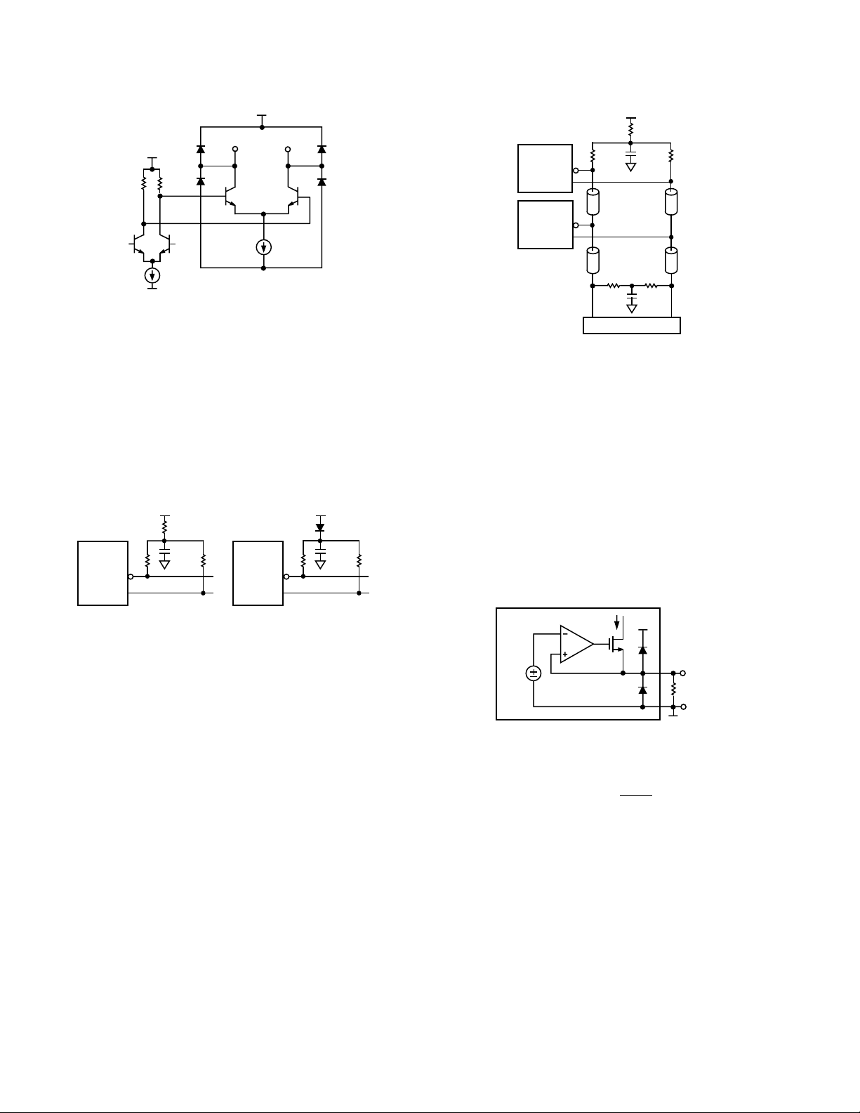
Figure 11. Simplified Output Circuit
To ensure proper operation, all outputs (including unused output)
must be pulled high using external pull-up networks to a level
within the output compliance range. If outputs from multiple
AD8151s are wired together, a single pull-up network may be
used for each output bus. The pull-up network should be chosen
to keep the output voltage levels within the output compliance
range at all times. Recommended pull-up networks to produce
PECL/ECL 100 kΩ and 10 kΩ compatible outputs are shown
in Figure 12. Alternatively, a separate supply can be used to
provide V
AD8151
OUTyyN
OUTyyP
; making R
COM
R
V
CC
L
and D
COM
R
COM
V
COM
R
L
unnecessary.
COM
AD8151
OUTyyN
OUTyyP
V
CC
D
COM
V
R
COM
L
R
L
V
CC
R
COM
AD8151 R
OUTyyN
OUTyyP
AD8151
OUTyyN
OUTyyP
L
Z
O
Z
O
R
L
RECEIVER
V
R
COM
L
Z
O
Z
O
R
L
Figure 13. Double Termination of AD8151 Outputs
In this case, the output levels are:
V
= V
OH
VOL = V
V
= VOH – VOL = (1/2) I
SWING
COM
COM
– (1/4) I
– (3/4) I
OUTRL
OUTRL
OUTRL
Output Current Set Pin (REF)
A simplified schematic of the reference circuit is shown in Figure 14. A single external resistor connected between the REF
pin and V
determines the output current for all output stages.
EE
This feature allows a choice of pull-up networks and transmission
line characteristic impedances while still achieving a nominal
output swing of 800 mV. At low data rates, substantial power
savings can be achieved by using lower output swings and higher
load resistances.
Figure 12. Output Pull-Up Networks: a) ECL 100 kΩ,
b) ECL 10 k
Ω
The output levels are simply:
V
= V
OH
COM
VOL = V
V
= VOH – VOL = I
SWING
V
= VCC – I
COM
V
= VCC – V (D
COM
The common-mode adjustment element (R
– I
COM
OUTRCOM
COM
OUTRL
OUTRL
(100 kΩ Mode)
) (10 kΩ Mode)
or D
COM
COM
) may
be omitted if the input range of the receiver includes the positive
supply voltage. The bypass capacitors reduce common-mode
perturbations by providing an ac short from the common nodes
) to ground.
(V
COM
When busing together the outputs of multiple AD8151s or when
running at high data rates, double termination of its outputs is
recommended to mitigate the impact of reflections due to open
transmission line stubs and the lumped capacitance of the
AD8151 output pins. A possible connection is shown in Figure
13; the bypass capacitors provide an ac short from the common
nodes of the termination resistors to ground. To maintain signal
fidelity at high data rates, the stubs connecting the output pins
to the output transmission lines or load resistors should be as
short as possible.
AD8151
1.2V
I
OUT
/20
V
CC
REF
R
SET
V
EE
Figure 14. Simplified Reference Circuit
The nominal output current is given by the following expression:
V
I
OUT
The minimum set resistor is R
I
OUT,MAX
4.8 kΩ resulting in I
= 25 mA. The maximum set resistor is R
OUT,MIN
tial output swing can be achieved in a 50 Ω load using R
1.5 kΩ (I
using R
= 16 mA), or in a doubly-terminated 75 Ω load
OUT
= 1.13 kΩ (I
SET
OUT
12.
=
20
R
SET
= 960 Ω resulting in
SET,MIN
SET,MAX
=
= 5 mA. Nominal 800 mV differen-
=
SET
= 21.3 mA).
To minimize stray capacitance and avoid the pickup of unwanted
signals, the external set resistor should be located close to the
REF pin. Bypassing the set resistor is not recommended.
–18–
REV. 0
AD8151
DATA
PATHS
CONTROL
LOGIC
+3.3V TO +5V
+3.3V TO +5V
V
SS
V
EE
GND GND
0.1F
(ONE FOR EACH V
CC
PIN,
4 REQUIRED)
0.1F
AD8151
V
DD
V
CC
Power Supplies
There are several options for the power supply voltages for the
AD8151, as there are two separate sections of the chip that require
power supplies. These are the control logic and the high-speed
data paths. Depending on the system architecture, the voltage
levels of these supplies can vary.
Logic Supplies
The control (programming) logic is CMOS and is designed to
interface with any of the various standard single-ended logic
families (CMOS or TTL). Its supply voltage pins are V
170, logic positive) and V
(Pin 152, logic ground). In all cases
SS
DD
(Pin
the logic ground should be connected to the system digital ground.
V
should be supplied at between 3.3 V to 5 V to match the
DD
supply voltage of the logic family that is used to drive the logic
inputs. V
capacitor. The absolute maximum voltage from V
should be bypassed to ground with a 0.1 µF ceramic
DD
DD
to V
SS
is 5.5 V.
Data Path Supplies
The data path supplies have more options for their voltage levels. The choices here will affect several other areas, like power
dissipation, bypassing, and common mode levels of the inputs
and outputs. The more positive voltage supply for the data paths
(Pins 41, 98, 149 and 171). The more negative supply is
is V
CC
, which appears on many pins that will not be listed here.
V
EE
The maximum allowable voltage across these supplies is 5.5 V.
The first choice in the data path power supplies is to decide
whether to run the device as ECL (Emitter-Coupled Logic) or
PECL (Positive ECL). For ECL operation, V
potential, while V
will be at a negative supply between –3.3 V
EE
will be at ground
CC
to –5 V. This will make the common-mode voltage of the inputs
and outputs at a negative voltage, see Figure 15.
+3.3V TO +5V
0.1F
AD8151
V
DD
CONTROL
LOGIC
V
SS
GND
GND
DATA
PATHS
V
CC
V
EE
0.1F
(ONE FOR EVERY TWO V
EE
PINS)
the part is to be ac-coupled, it is not necessary to have the input/
output common mode at the same level as the other system
circuits, but it will probably be more convenient to use the same
supply rails for all devices.
For PECL operation, V
will be at ground potential and V
EE
CC
will be a positive voltage from 3.3 V to 5 V. Thus, the common
mode of the inputs and outputs will be at a positive voltage.
These can then be dc-coupled to other PECL operated devices.
If the data paths are ac-coupled, then the common-mode levels
do not matter, see Figure 16.
Figure 16. Power Supplies and Bypassing for PECL
Operation
POWER DISSIPATION
For analysis, the power dissipation of the AD8151 can be divided
into three separate parts. These are the control logic, the data
path circuits and the (ECL or PECL) outputs, which are part of
the data path circuits, but can be dealt with separately. The first
of these, the control logic, is CMOS technology and does not
dissipate a significant amount of power. This power will, of
course, be greater when the logic supply is 5 V rather than 3 V,
but overall it is not a significant amount of power and can be
ignored for thermal analysis.
AD8151
V
DD
CONTROL
LOGIC
I, DATA PATH
LOGIC
V
SS
V
EE
V
CC
DATA
PATHS
I
OUT
V
OUT
R
OUT
LOW – V
EE
If the data paths are to be dc-coupled to other ECL logic devices
that run with ground as the most positive supply and a negative
voltage for V
REV. 0
–3.3V TO –5V
Figure 15. Power Supplies and Bypassing for ECL
Operation
, then this is the proper way to run. However, if
EE
GND GND
Figure 17. Major Power Consumption Paths
The data path circuits operate between the supplies VCC and
V
. As described in the power supply section, this voltage can
EE
range from 3.3 V to 5 V. The current consumed by this section
will be constant, so operating at a lower voltage can save about
35 percent in power dissipation.
–19–

AD8151
The power dissipated in the data path outputs is affected by several
factors. The first is whether the outputs are enabled or disabled.
The worst case occurs when all of the outputs are enabled.
The current consumed by the data path logic can be approximated by:
I
= 35 mA + [4.5 mA + (I
CC
/20 mA × 3 mA)]
OUT
× (# of outputs enabled)
This says that there will always be a minimum of 35 mA flowing. I
will increase by a factor that is proportional to both the
CC
number of enabled outputs and the programmed output current.
The power dissipated in this circuit section will simply be the
voltage of this section (V
case, assume that V
– VEE) times the current. For a worst
CC
– VEE is 5.0 V, all outputs are enabled
CC
and the programmed output current is 25 mA. The power dissipated by the data path logic will be:
P = 5.0 V {35 mA + [4.5 mA + (25 mA/20 mA × 3 mA)]
× 17} = 876 mW
The power dissipated by the output current depends on several
factors. These are the programmed output current, the voltage
drop from a logic low output to V
and the number of enabled
EE
outputs. A simplifying assumption is that one of each (enabled)
differential output pair will be low and draw the full output
current (and dissipate most of the power for that output), while
the complementary output of the pair will be high and draw
insignificant current. Thus, its power dissipation of the high
output can be ignored and the output power dissipation for each
output can be assumed to occur in a single static low output
that sinks the full output-programmed current.
The voltage across which this current flows can also vary, depending on the output circuit design and the supplies that are used
for the data path circuitry. In general, however, there will be a
voltage difference between a logic low signal and V
. This is
EE
the drop across which the output current flows. For a worst
case, this voltage can be as high as 3.5 V. Thus, for all outputs
enabled and the programmed output current set to 25 mA, the
power dissipated by the outputs:
P = 3.5 V (25 mA) × 17 = 1.49 W
HEAT SINKING
Depending on several factors in its operation, the AD8151 can
dissipate upwards of 2 W or more. The part is designed to operate without the need for an explicit external heatsink. However,
the package design offers enhanced heat removal via some of the
package pins to the PC board traces.
The V
pins on the input sides of the package (Pins 1 to 46 and
EE
Pins 93 to 138) have “finger” extensions inside the package
that connect to the “paddle” upon which the IC chip is mounted.
These pins provide a lower thermal resistance from the IC to
pins than other pins that just have a bond wire. As a
the V
EE
result these pins can be used to enhance the heat removal process from the IC to the circuit board and ultimately to the ambient.
The V
pins described above should be connected to a large area
EE
of circuit board trace material in order to take most advantage
their lower thermal resistance. If there is a large area available
on an inner layer that is at V
potential, then vias can be pro-
EE
vided from the package pin traces to this layer. There should be
no thermal-relief pattern when connecting the vias to the inner
layers for these V
pins. Additional vias in parallel and close to
EE
the pin leads can provide an even lower thermal resistive path. If
possible to use, 2 oz. copper foil will provide better heat removal
than 1 oz.
The AD8151 package has a specified thermal impedance θ
of
JA
30°C/W. This is the worst case, still-air value that can be expected
when the circuit board does not significantly enhance the heat
removal from the package. By using the concept described above
or by using forced-air circulation, the thermal impedance can be
lowered.
For an extreme worst case analysis, the junction rise above the
ambient can be calculated assuming 2 W of power dissipation
of 30°C/W to yield a 60°C rise above the ambient. There
and θ
JA
are many techniques described above that can mitigate this situation. Most actual circuits will not result in this high a rise of the
junction temperature above the ambient.
APPLICATIONS
AD8151 INPUT AND OUTPUT BUSING
Although the AD8151 is a digital part, in any application that
runs at high speed, analog design details will have to be given very
careful consideration. At high data rates, the design of the signal
channels will have a strong influence on the data integrity and
its associated jitter and ultimately bit error rate (BER).
While it might be considered very helpful to have a suggested
circuit board layout for any particular system configuration,
this is not something that can be practically realized. Systems
come in all shapes, sizes, speeds, performance criteria and cost
constraints. Therefore, some general design guidelines will be
presented that can be used for all systems and judiciously modified where appropriate.
High-speed signals travel best, i.e. maintain their integrity, when
they are carried by a uniform transmission line that is properly
terminated at either end. Any abrupt mismatches in impedance
or improper termination will create reflections that will add to
or subtract from parts of the desired signal. Small amounts of
this effect are unavoidable, but too much will distort the signal
to the point that the channel BER will increase. It is difficult to
fully quantify these effects, because they are influenced by many
factors in the overall system design.
A constant-impedance transmission line is characterized by
having a uniform cross-section profile over its entire length. In
particular, there should be no “stubs,” which are branches that
intersect the main run of the transmission line. These can have
an electrical “appearance” that is approximated by a lumped
element, such as a capacitor, or if long enough, as another transmission line. To the extent that stubs are unavoidable in a design,
their effect can be minimized by making them as short as possible and as high an impedance as possible.
Figure 13 shows a differential transmission line that connects
two differential outputs from AD8151s to a generic receiver. A
more generalized system can have more outputs bused, and
more receivers on the same bus, but all the same concepts apply.
The inputs of the AD8151 can also be considered as a receiver.
The transmission lines that bus all of the devices together are
shown with terminations at each end.
The individual outputs of the AD8151 are stubs that intersect
the main transmission line. Ideally, their current-source outputs
would be infinite impedance, and they would have no effect on
signals that propagate along the transmission line. In reality, each
–20–
REV. 0

AD8151
external pin of the AD8151 projects into the package, and has a
bond wire connected to the chip inside. On-chip wiring then
connects to the collectors of the output transistors and to ESD
protection diodes.
Unlike some other high-speed digital components, the AD8151
does not have on-chip terminations. While this location would
be closer to the actual end of the transmission line for some
architectures, this concept can limit system design options. In
particular, it is not possible to bus more than two inputs or
outputs on the same transmission line and it is also not possible
to change the value of these terminations to use for different
impedance transmission lines. The AD8151, with the added
ability to disable its outputs, is much more versatile in these
types of architectures.
If the external traces are kept to a bare minimum, then the
output will present a mostly lumped capacitive load of about
2 pF. A single stub of 2 pF will not seriously adversely affect
signal integrity for most transmission lines, but the more of
these stubs, the more adverse their influence will be.
One way to mitigate this effect is to locally reduce the capacitance
of the main transmission line near the point of stub intersection.
Some practical means for doing this are to narrow the PC board
traces in the region of the stub and/or to remove some of the
ground plane(s) near this intersection. The effect of these techniques will locally lower the capacitance of the main transmission
line at these points, while the added capacitance of the AD8151
outputs will “compensate” for this reduction in capacitance.
The overall intent is to create as uniform a transmission line as
possible.
In selecting the location of the termination resistors it is important to keep in mind that, as their name implies, they should be
placed at either end of the line. There should be no or minimal
projection of the transmission line beyond the point where the
termination resistors connect to it.
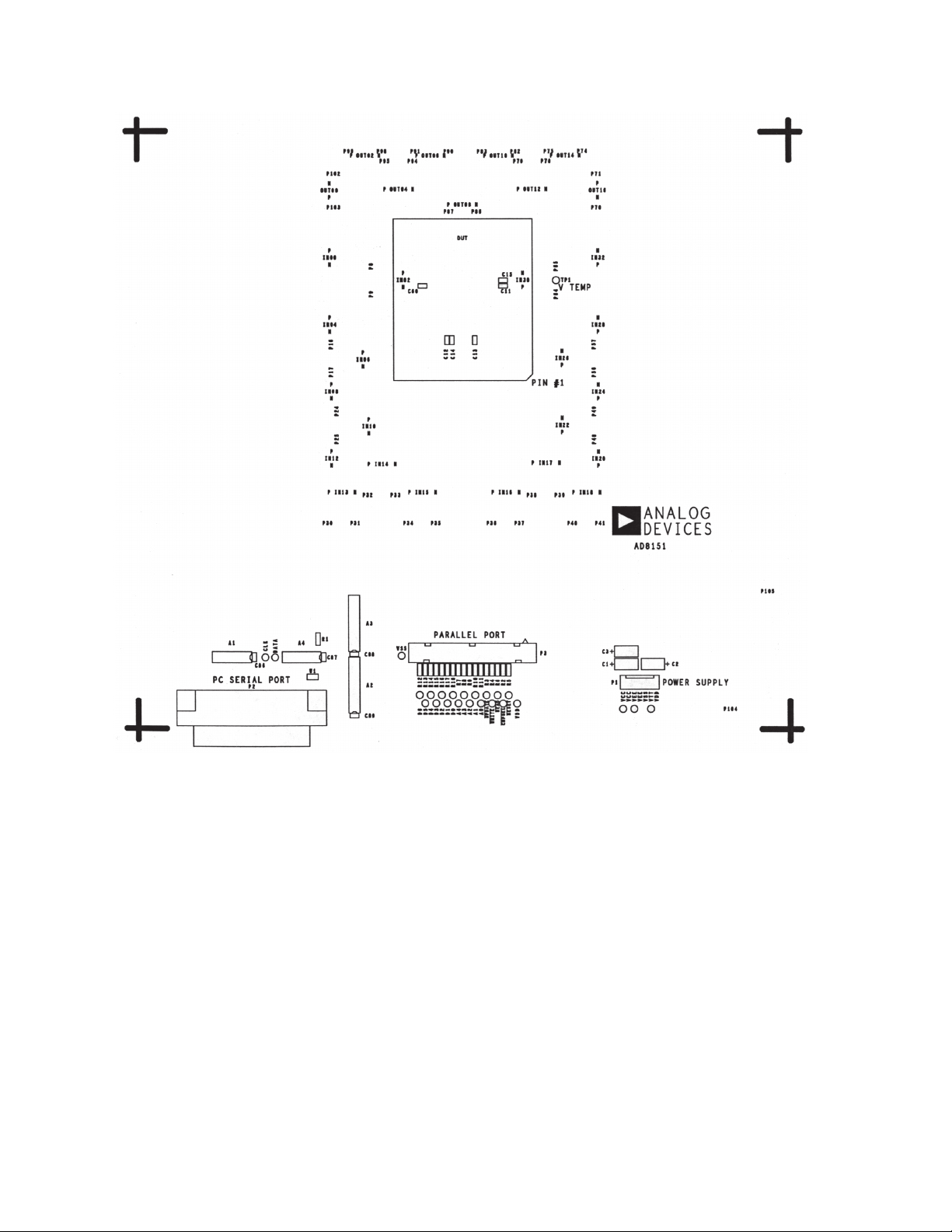
EVALUATION BOARD
An evaluation board has been designed and is available to rapidly
test the main features of the AD8151. This board lets the user
analyze the analog performance of the AD8151 channels and
easily control the configuration of the board by a standard PC.
The board has limited numbers of differential input/output
pairs. Each differential pair of microstrip is connected to either
top-mount or side-launch SMA connectors. The top-mount
SMA connectors are drilled and stubbed for superior performance. The FR4 type board contains a total of nine outputs (all
even numbered outputs) and 20 inputs (numbers 0, 2, 4, 6, 8,
10, 12, 13, 14, 15, 16, 17, 18, 20, 22, 24, 26, 28, 30, 32). It is
important to note that the shells of the SMA connectors are
attached to VCC. This makes only ECL or negative level swings
possible during testing.
Power Supplies
The AD8151 is designed to work with standard ECL logic levels.
This means that V
The shells of the I/O SMA connectors are at V
is at ground and VEE is at a negative supply.
CC
potential. Thus,
CC
when operating in the standard ECL configuration, test equipment
can be directly connected to the board, as the test equipment
will have its connector “shells” at ground potential also.
Operating in PECL mode requires V
age, while V
is at ground. Since this would make the shells of
EE
to be at a positive volt-
CC
the I/O connectors at a positive voltage, it can cause problems
when directly connecting to test equipment. Some equipment,
such as battery-operated oscilloscopes, can be “floated” from
ground, but care should be taken with line-powered equipment
to avoid creating a dangerous situation. Refer to the manual of
the test equipment that is being used.
The voltage difference from V
to VEE can range from 3 V to
CC
5 V. Power savings can be realized by operating at a lower voltage without any compromise in performance.
A separate connection is provided for V
potential of the outputs. This can be at a voltage as high as V
but power savings can be realized if V
, the termination
TT
is at a voltage that is
TT
CC
,
somewhat lower. Please consult elsewhere in the data sheet for
the specification for the limits of the V
supply.
TT
As a practical matter, current on the evaluation board will flow
from the V
multiple outputs of the AD8151, and on to the V
running in ECL mode, V
supply, through the termination resistors, into the
TT
will want to be at a negative supply.
TT
supply. When
EE
Most power supplies will not allow their ground connection to
V
and then the negative supply to VTT. This will require them
CC
to source current from their negative supply, which wants to
flow to the more-negative V
to the ground terminal of the V
referenced to V
when running in ECL mode or a true bipolar
EE
. This current will not then return
EE
supply. Thus, VTT should be
TT
supply should be used.
The digital supply is provided to the AD8151 by the V
V
pins. VSS should always be at ground potential to make it
SS
compatible with standard CMOS or TTL logic. V
DD
can range
DD
and
from 3 V to 5 V, and should be matched to the supply voltage of
the logic used to control the AD8151. However, since PCs use
5 V logic on their parallel port, V
should be at 5 V when using a
DD
PC to program the AD8151.
Bypassing
Most of the board’s bypass capacitors are opposite the DUT on
the solder side, connected between V
and VEE. This is where
CC
they will be most effective. These capacitors are 0.01 µF ceramic
chip capacitors for low inductance. There are additional higher
value capacitors elsewhere on the board for bypassing at lower
frequencies. The location of these is not as critical.
Input and Output Considerations
Each input contains a 100 Ω differential termination. Although
the differential termination eases board layout due to its compact
nature, it can cause problems with the driving generator. A typical
pulse or pattern generator wants to see 50 Ω to ground (or to
–2 V in some cases). High speed probing of the input showed if
this type of termination is not present then input amplitudes could
be slightly off. Even more affected can be the dc input levels.
Depending on the generator used, these levels can be off as much
as 800 mV in either direction. A correction for this problem is to
attach a 6 dB attenuator to each P and N input. Because the
AD8151 has a large common-mode voltage range on its input
stage, it will not be significantly affected by dc level errors.
REV. 0
–21–

AD8151
On this evaluation board all unused inputs are tied to VCC (GND).
All outputs, whether brought out to connectors or not, are tied
to V
through a 49.9 Ω resistor. The AD8151 device is on the
TT
component side of the board, while input terminations and output
back terminations are on the circuit side. The input signals from
the circuit side transit through via holes to the DUT’s pads. The
component-side output signals connect to via holes and to
circuit-side 49.9 Ω termination resistors.
Board Construction
For this board FR4 material was chosen over more exotic board
materials. Tests showed exotic materials to be unnecessary. This
is a 4-layer board. Power is bused on both external and internal
layers. Test structures showed microstrip performance to be
unaffected by the dc bias levels on the plane beneath it.
The manufacturing process should produce a controlledimpedance board. The board stack consists of a 5-mil-thick
layer between external and internal layers. This allows the use of
an 8-mil-wide microstrip trace running from SMA connector to
the DUT’s pads. The narrow trace avoids the need to neck down
the trace width as DUT’s pads are approached and it helps to
control the microstrip trace impedance. The thin 5-mil dielectric
also helps to control crosstalk by way of confining the electromagnetic fields more between the trace and the plane below.
Configuration Programming
The board is configurable by one of two methods. For ease of
use, custom software is provided that controls the AD8151
programming via the parallel port of a PC. This requires a usersupplied standard printer cable that has a DB-25 connector at
one end (parallel- or printer-port interface) and a Centronixtype connector at the other that connects to P2 of the AD8151
evaluation board. The programming with this scheme is done in
a serial fashion, so it is not the fastest way to configure the AD8151
matrix. However, the user interface makes it very convenient to
use this programming method.
If a high-speed programming interface is desired, the AD8151
address and data buses are directly available on P3. The source
of the program signals can be a piece of test equipment, like the
Tektronix HFS-9000 digital test generator, or some other usersupplied hardware that generates programming signals.
When using the PC interface, the jumper at W1 should be
installed and no connections should be made to P3. When using
the P3 interface, no jumper is installed at W1. There are locations for termination resistors for the address and data signals if
these are necessary.
Software Installation
The software to operate the AD8151 is provided on two 3.5"
floppy disks. The software is installed by inserting Disk 1 into
the floppy drive of a PC and running the “setup.exe” program.
This will routinely install the software and prompt the user
when to change to Disk 2. The setup program will also prompt
the user to select the directory for the program.
After running the software, the user will be prompted to identify
which (of three) software driver is used with the PC’s parallel
port. The default is LPT1, which is most commonly used. However, some laptops commonly use the PRN driver. It is also
possible that some systems are configured with the LPT2 driver.
If it is not known which driver is used, it is best to select LPT1
and proceed to the next screen. This will show a full array of
“buttons” that allows the connection of any input to output of
the AD8151. All of the outputs should be in the output “OFF”
state right after the program starts running. Any of the active
buttons can be selected with a mouse click, which will send out
one burst of programming data.
After this, the PC keyboard’s left or right arrow keyboard key
can be held down to generate a steady stream of programming
signals out of the parallel port. The CLOCK test point on the
AD8151 evaluation board can be monitored with an oscilloscope for any activity (user-supplied printer cable must be
connected). If there is a square-wave present, the proper software driver is selected for the PC’s parallel port.
If there is no signal present, another driver should be tried by
selecting the Parallel Port menu item under the “File” pulldown menu selection just under the title bar. Select a different
software driver and carry out the above test until signal activity
is present at the CLOCK test point.
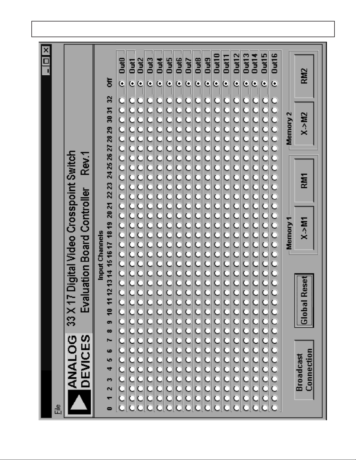
Software Operation
Any button can be clicked in the matrix to program the input to
output connection. This will send the proper programming
sequence out the PC parallel port. Since only one input can be
programmed to a given output at one time, clicking a button in
a horizontal row will cancel the other selection that is already
selected in that row. However, any number of outputs can share
the same input.
A shortcut for programming all outputs to the same input is to
use the broadcast feature. After clicking on the Broadcast Connection button, a screen will appear that will prompt for the
user to select which input should be connected to all outputs.
The user should type in an integer from 0 to 32 and then click
on OK. This will send out the proper program data and return
to the main screen with a full column of buttons selected under
the chosen input.
The Off column can be used to disable to whichever output one
chooses. To disable all outputs, the Global Reset button can be
clicked. This will select the full column of OFF buttons.
Two scratch-pad memories (Memory 1 and Memory 2) are
provided to conveniently save a particular configuration. However, these registers are erased when the program is terminated.
For long-term storage of configurations, the disk-storage memory
should be used. The Save and Load selections can be accessed
from the “File” pull-down menu under the title bar.
–22–
REV. 0
AD8151
AD8151
REV. 0
Figure 18. Evaluation Board Controller
–23–
AD8151
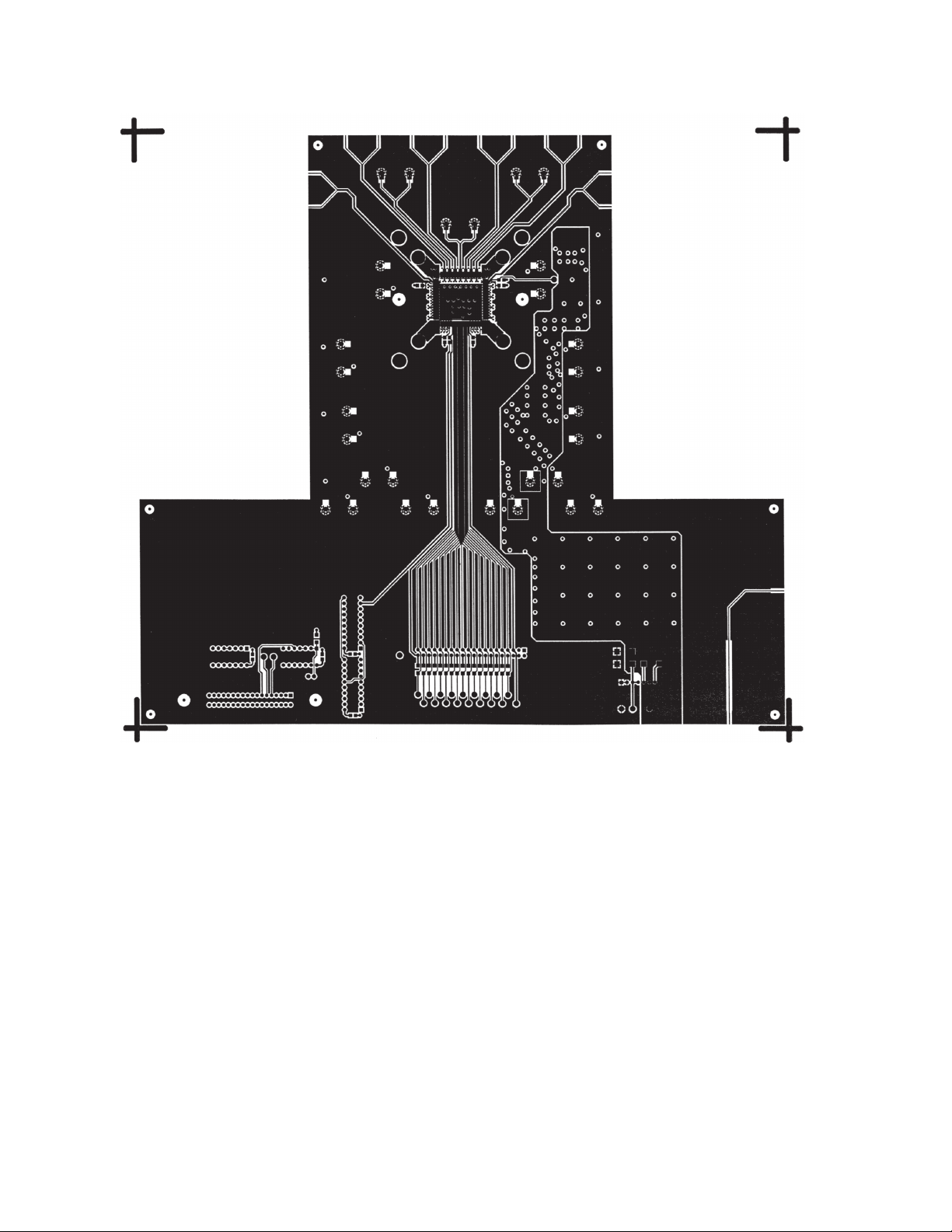
Figure 19. Component Side
–24–
REV. 0
AD8151
REV. 0
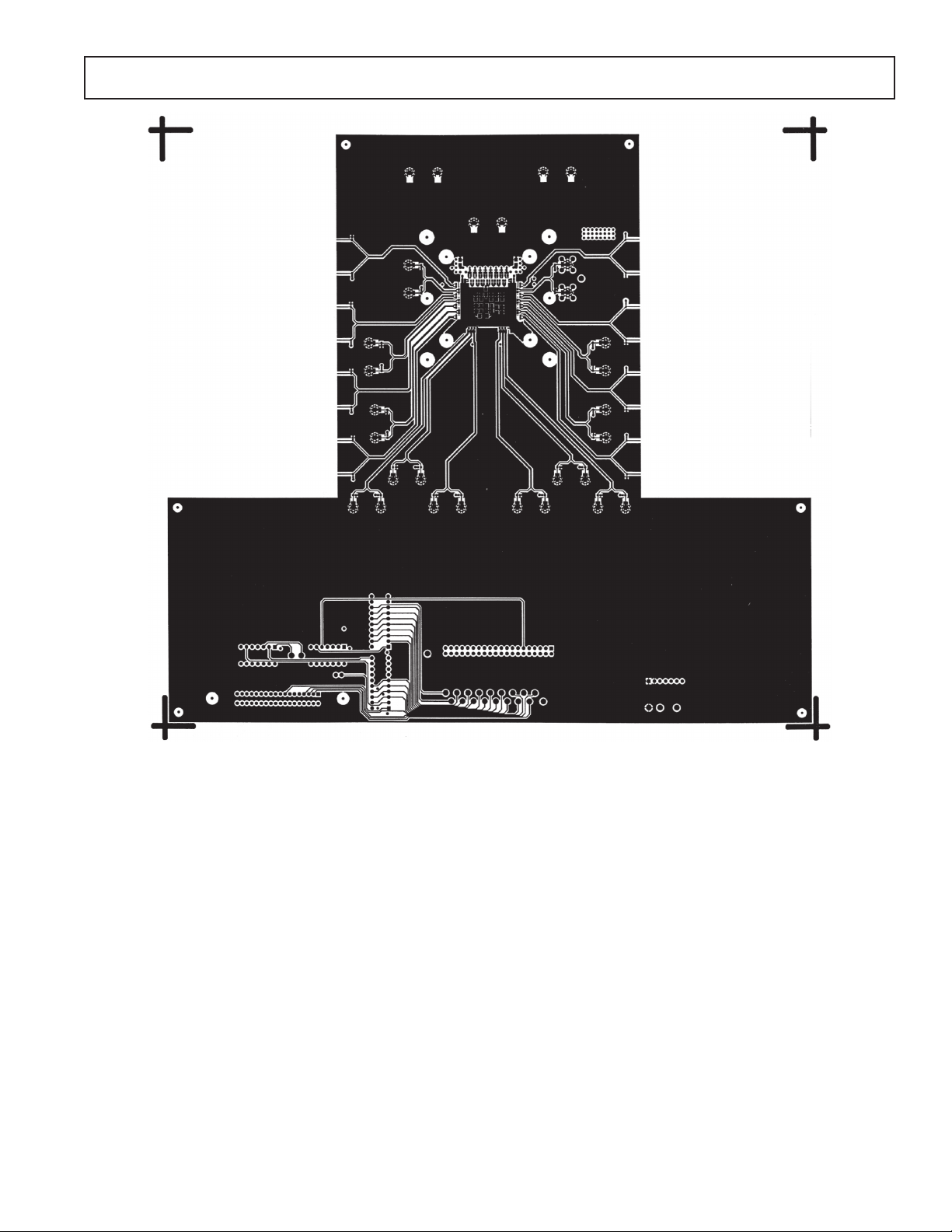
Figure 20. Circuit Side
–25–
AD8151
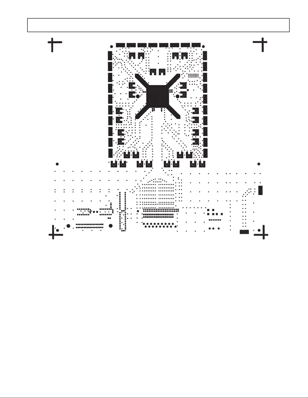
Figure 21. Silkscreen Top
–26–
REV. 0
AD8151
REV. 0
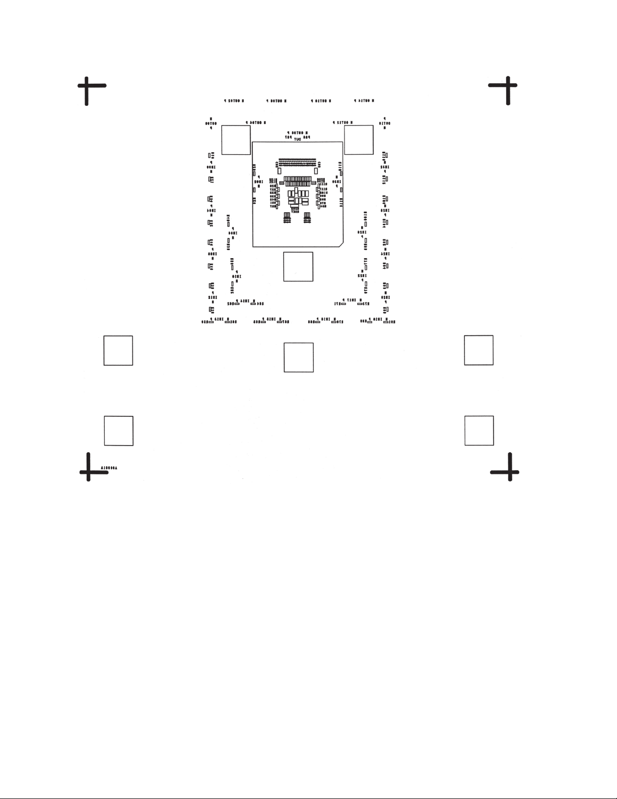
Figure 22. Soldermask Top
–27–
AD8151
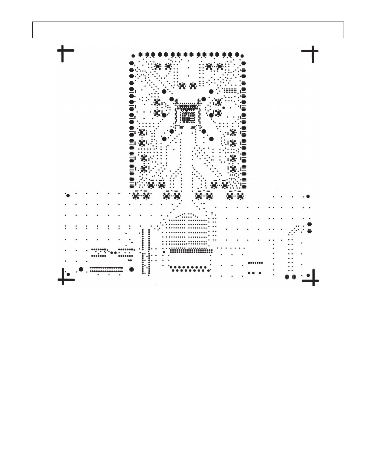
Figure 23. Silkscreen Bottom
–28–
REV. 0
AD8151
REV. 0
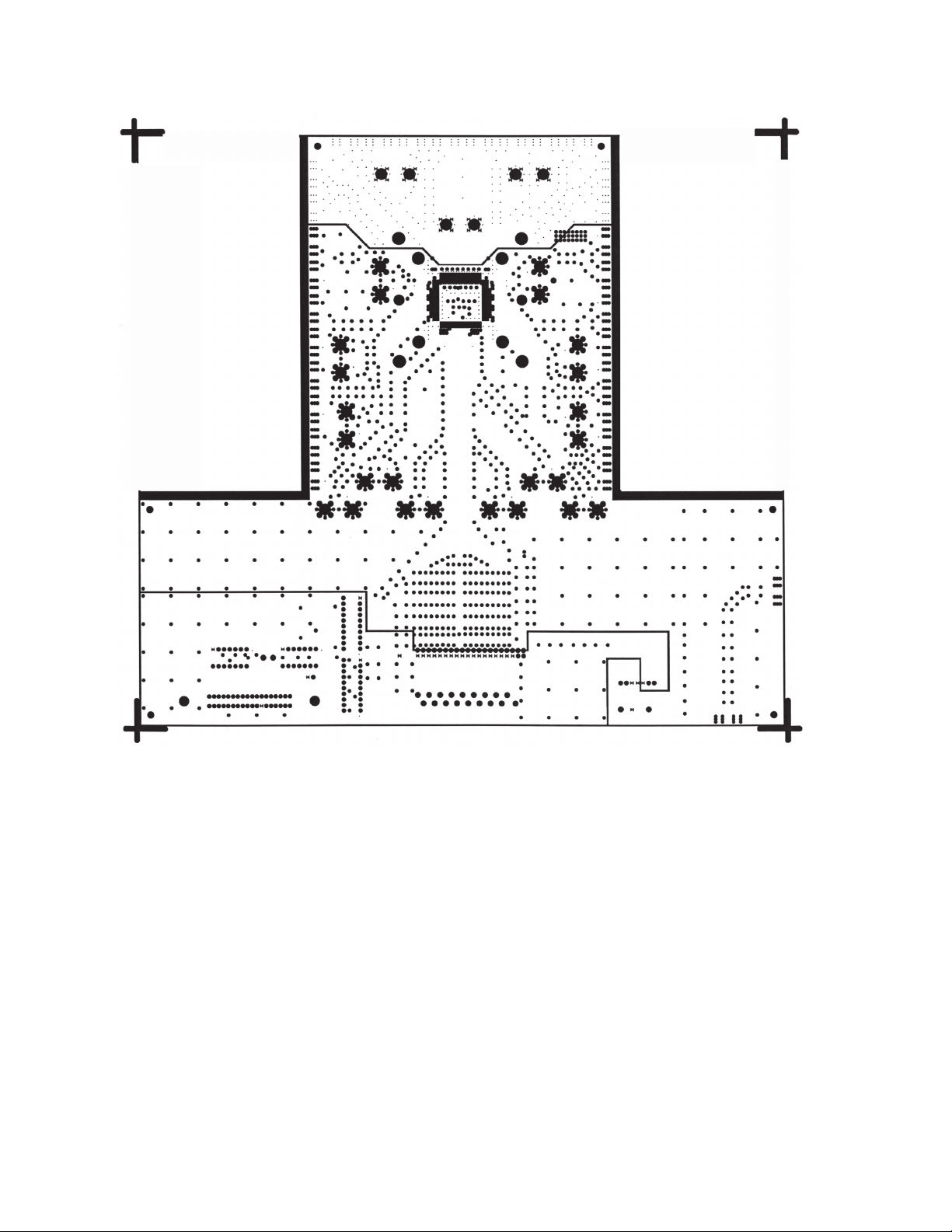
Figure 24. Soldermask Bottom
–29–
AD8151
Figure 25. INT1 (VEE)
–30–
REV. 0
AD8151
REV. 0
Figure 26. INT2 (VCC)
–31–
AD8151
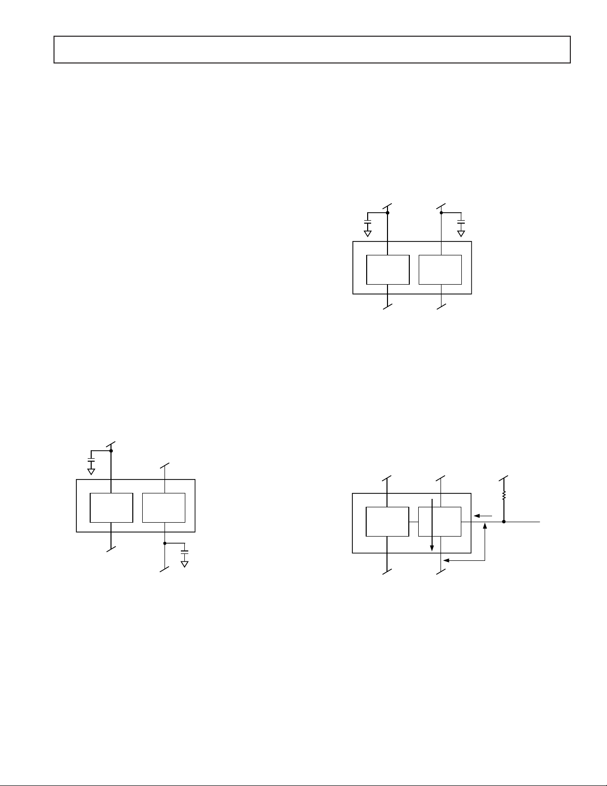
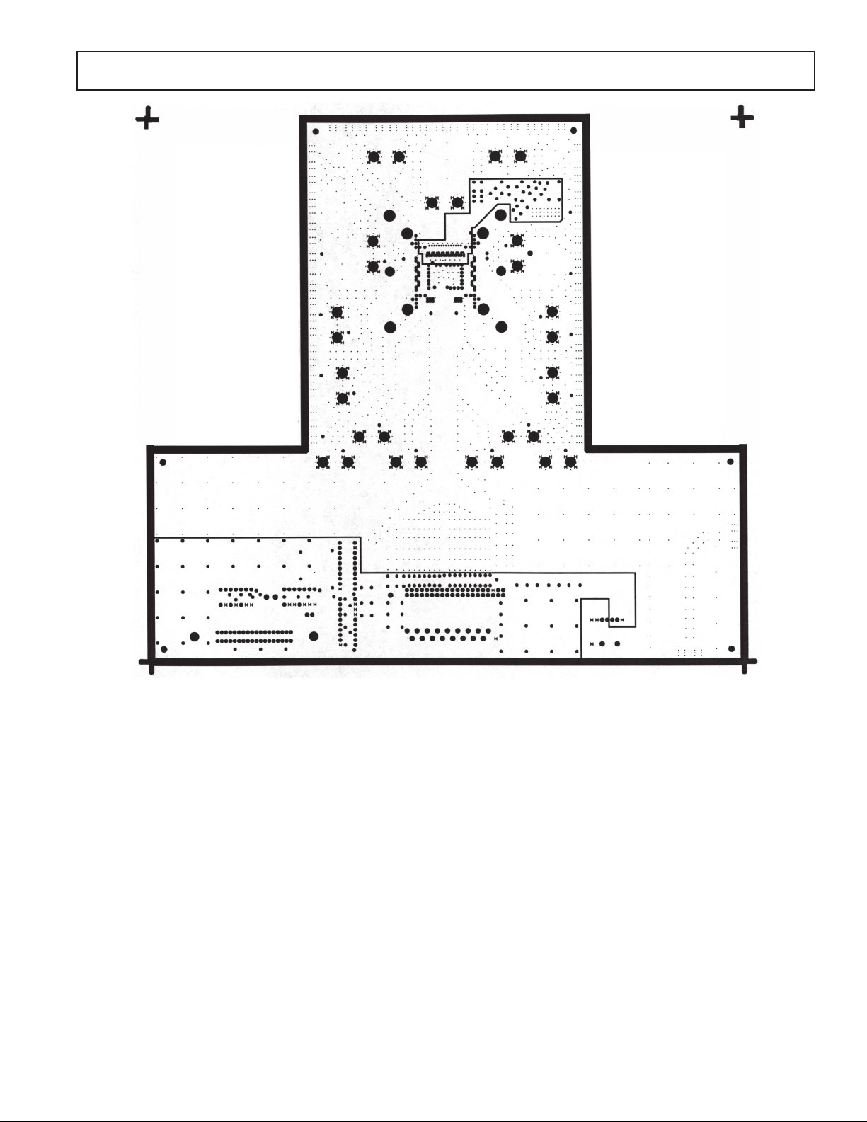
C31
0.01F
V
CC
V
EE
V
EE
V
CC
C32
0.01F
C11
0.01F
V
CC
V
EE
V
EE
OUT16N
V
CC
OUT16P
C15
0.01F
V
IN20P
IN20N
IN21P
IN21N
IN22P
IN22N
V
IN23P
IN23N
V
IN24P
IN24N
V
IN25P
IN25N
V
IN26P
IN26N
V
IN27P
IN27N
V
IN28P
IN28N
V
IN29P
IN29N
V
IN30P
IN30N
V
IN31P
IN31N
V
IN32P
IN32N
V
V
V
EE
EE
EE
EE
EE
EE
EE
EE
EE
EE
EE
EE
EE
EE
C29
0.01F
VEEV
CC
C6
IN17N
IN17P
176
175
0.01F
VEEV
IN16N
IN16P
174
173
CC
C7
0.01F
V
V
CC
DD
V
170
172
171
59
V
V
CC
EE
C5
0.01F
V
V
EE
CC
C4
0.01F
V
V
EE
CC
IN19N
IN19P
IN18N
IN18P
184
183
182
181
180
179
178
177
1
2
PIN 1
3
IDENTIFIER
4
5
6
7
8
9
10
11
12
13
14
15
16
17
18
19
20
21
22
23
24
25
26
27
28
29
30
31
32
33
34
35
36
37
38
39
40
41
42
43
44
45
46
474849505152535455565758606162636465666768
EE
C13
0.01F
RESET
169
CSREWE
168
167
166
UPDATE
A0A1A2A3A4D0D1
165
164
163
160
162
161
AD8151
184L LQFP
TOP VIEW
(Not to Scale)
69
70717274757677
159
158
73
C14
0.01F
D2D3D4
157
156
V
EE
C12
0.01F
R203
1.5k
V
V
SS
DD
D5
D6
155
154
153
152
78
79808182848586
V
151
V
CC
VEEV
CC
C8
150
149
148
0.01F
VEEV
IN15N
IN15P
147
146
CC
C9
0.01F
VEEV
IN14N
IN14P
145
144
143
142
87838889909192
CC
C10
0.01F
VEEV
IN13N
IN13P
141
140
139
138
137
136
135
134
133
132
131
130
129
128
127
126
125
124
123
122
121
120
119
118
117
116
115
114
113
112
111
110
109
108
107
106
105
104
103
102
101
100
CC
99
98
97
96
95
94
93
C30
0.01F
V
EE
IN12N
IN12P
V
EE
IN11N
IN11P
V
EE
IN10N
IN10P
V
EE
IN09N
IN09P
V
EE
IN08N
IN08P
V
EE
IN07N
IN07P
V
EE
IN06N
IN06P
V
EE
IN05N
IN05P
V
EE
IN04N
IN04P
V
EE
IN03N
IN03P
V
EE
IN02N
IN02P
V
EE
IN01N
IN01P
V
EE
IN00N
IN00P
V
EE
V
EE
OUT00P
OUT00N
V
EE
V
EE
V
CC
C60
0.01F
V
EE
EE
EE
V
VEEV
OUT15P
OUT15N
EE
OUT14P
OUT14N
VEEVEEVEEVEEVEEVEEVEEVEEVEEVEEV
OUT13P
OUT13N
OUT12P
OUT12N
OUT11N
OUT10P
OUT10N
OUT09P
OUT09N
OUT08P
OUT08N
OUT07P
OUT07N
OUT06P
OUT06N
OUT05P
OUT05N
OUT04N
OUT11P
Figure 27. Bypassing Schematic
–32–
OUT04P
OUT03N
EE
OUT03P
OUT02N
EE
V
OUT02P
OUT01N
EE
V
OUT01P
REV. 0
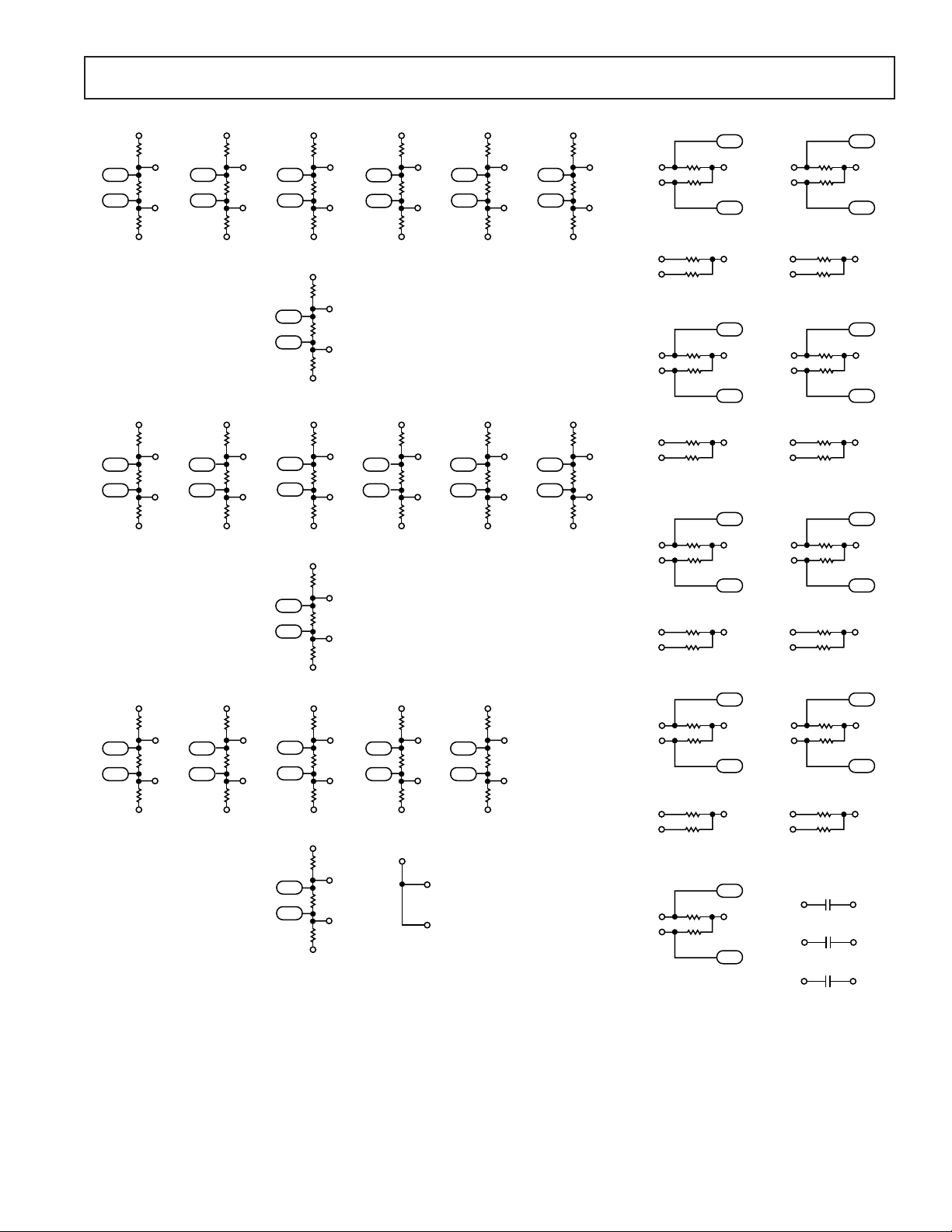
AD8151
R19
1.65k
P4
P5
R21
1.65k
R28
1.65k
P8
P9
R26
1.65k
R34
1.65k
P12
P13
R32
1.65k
R40
1.65k
P16
P17
R38
1.65k
R44
1.65k
P20
P21
R46
1.65k
R50
1.65k
P24
P25
R52
1.65k
V
CC
IN06P
R39
105
IN06N
V
EE
V
CC
IN08P
R45
105
IN08N
V
EE
V
CC
IN10P
R51
105
IN10N
V
EE
R58
1.65k
P28
P29
R56
1.65k
R59
1.65k
P30
P31
R61
1.65k
R62
1.65k
P32
P33
R64
1.65k
R65
1.65k
P34
P35
R67
1.65k
R68
1.65k
P36
P37
R70
1.65k
R71
1.65k
P38
P39
R73
1.65k
V
CC
IN12P
R57
105
IN12N
V
EE
V
CC
R89
1.65k
P40
P41
R91
1.65k
V
CC
IN18P
R90
105
IN18N
V
EE
IN13P
R60
105
IN13N
V
EE
V
CC
IN14P
R63
105
IN14N
V
EE
V
CC
R85
1.65k
P44
P45
R83
1.65k
V
CC
IN20P
R84
105
IN20N
V
EE
IN15P
R66
105
IN15N
V
EE
V
CC
IN16P
R69
105
IN16N
V
EE
V
CC
IN17P
R72
105
IN17N
V
EE
R79
1.65k
P48
P49
R77
1.65k
V
CC
IN22P
R78
105
IN22N
V
EE
V
CC
P
IN01, IN03, IN05, IN07,
IN09, IN11, IN19, IN21,
IN23, IN25, IN27, IN29, IN31
N
V
CC
IN00P
R20
105
IN00N
V
EE
V
CC
IN02P
R27
105
IN02N
V
EE
V
CC
IN04P
R33
105
IN04N
V
EE
R94
1.65k
P52
P53
R92
1.65k
R98
1.65k
P56
P57
R100
1.65k
R104
1.65k
P60
P61
R106
1.65k
V
CC
IN24P
R93
105
IN24N
V
EE
V
CC
IN26P
R99
105
IN26N
V
EE
V
CC
IN28P
R105
105
IN28N
V
EE
R116
1.65k
P64
P65
R118
1.65k
R112
1.65k
P68
P69
R110
1.65k
V
CC
IN30P
R117
105
OUT08P
OUT08N
IN30N
V
EE
OUT09P
OUT09N
OUT10P
OUT10N
V
CC
OUT11P
IN32P
R111
105
OUT11
N
IN32N
V
EE
OUT12P
OUT12N
OUT13P
OUT13N
OUT14P
OUT14N
OUT15P
OUT15N
OUT16P
OUT16N
R160
49.9
R162
49.9
R165
49.9
R163
49.9
R175
49.9
R173
49.9
R170
49.9
R172
49.9
R185
49.9
R183
49.9
R180
49.9
R182
49.9
R195
49.9
R193
49.9
R190
49.9
R192
49.9
R200
49.9
R198
49.9
P87
P86
P83
P82
P79
P78
P75
P74
P71
P70
OUT00P
V
TT
OUT00N
OUT01P
V
TT
OUT01N
OUT02P
V
TT
OUT02N
OUT03P
V
TT
OUT03N
OUT04P
V
TT
OUT04N
OUT05P
V
TT
OUT05N
OUT06P
V
TT
OUT06N
OUT07P
V
TT
OUT07N
V
V
TT
TT
V
TT
V
TT
R121
49.9
R122
49.9
R125
49.9
R127
49.9
R130
49.9
R132
49.9
R135
49.9
R133
49.9
R140
49.9
R142
49.9
R145
49.9
R143
49.9
R150
49.9
R152
49.9
R155
49.9
R153
49.9
C16
0.01F
C82
0.01F
C83
0.01F
P103
P102
P99
P98
P95
P94
P91
P90
V
V
V
V
TT
V
TT
V
TT
V
TT
V
TT
V
TT
V
TT
V
TT
CC
CC
CC
REV. 0
Figure 28. Evaluation Board Input/Output Schematic
–33–
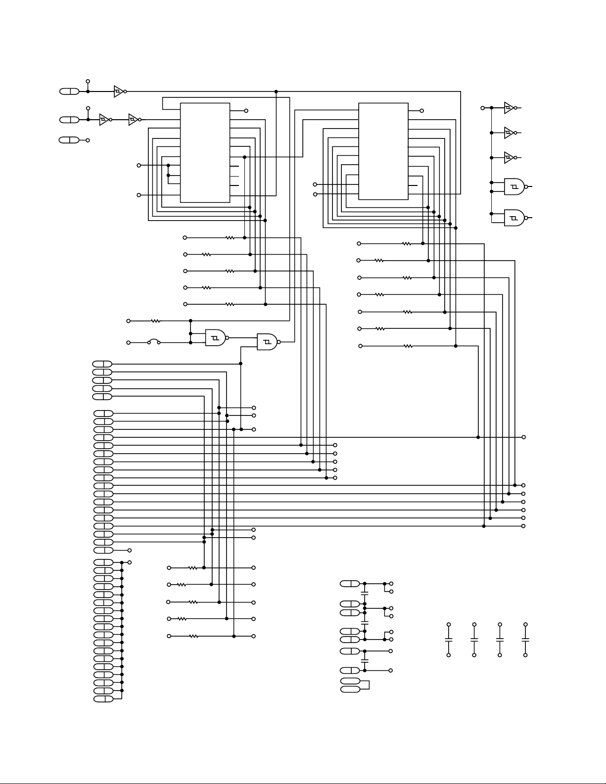
AD8151
CLK
CLK P2 6
DATA
P2 5
DATA
V
P2 25
SS
READ
RESET
WRITE
UPDATE
CHIP_SELECT
WRITE P3 13
RESET
READ P3 11
D0 P3 27
A4
A3
A2
A1 P3 19
A0
D6 P3 39
D5 P3 37
D4
D3
D2
D1
UPDATE P3 15
CHIP_SELECT P3 9
V
DD
V
SS
A1
2
1
74HC14
4
3
5
74HC14A174HC14
V
SS
V
DD
V
SS
V
DD
V
SS
P2 7
P2 3
P2 8
P2 4
P2 2
P3 7
P3 25
P3 23
P3 21
P3 17
P3 35
P3 33
P3 31
P3 29
P3 5
P3 14
P3 8
P3 12
P3 28
P3 26
P3 24
P3 22
P3 20
P3 18
P3 40
P3 38
P3 36
P3 34
P3 32
P3 30
P3 16
P3 10
P3 6
A1
9
74HC14
A1
11 10
74HC14
A1
13
74HC14
A4
9
10
74HC132
A4
12
13
74HC132
8
12
8
11
1
A1
6
R1
20k
W1
OUT_EN
2
D0
3
D1
4
D2
5
D3
A2
6
D4
74HC74 74HC74
7
D5
8
D6
9
D7
10
GND
V
SS
49.0
V
SS
V
SS
R10
49.0
V
SS
V
SS
1
2
74HC132
20
V
CC
Q0
Q1
Q2
Q3
Q4
Q5
Q6
Q7
CLK
R8
R7
49.0
R9
49.0
V
DD
19
18
17
16
15
14
13
12
11
V
DD
V
SS
160A4
161A3
162A2
163A1
R11
49.0
A4
3
164A0
A4
4
5
6
74HC132
1
OUT_EN
2
D0
3
D1
4
D2
5
D3
6
D4
7
D5
8
D6
9
D7
10
GND
V
SS
R13
49.0
V
SS
V
SS
R15
49.0
V
SS
V
SS
R17
49.0
V
SS
V
SS
20
V
A3
CLK
CC
Q0
Q1
Q2
Q3
Q4
Q5
Q6
Q7
R12
49.0
V
DD
19
18
17
16
15
14
13
12
11
V
153D6
DD
154D5
R14
49.0
155D4
156D3
R16
49.0
157D2
158D1
R18
49.0
159D0
TP5
TP6
TP4
TP20
TP9
TP10
TP11
TP12
TP13
TP14
TP15
TP16
TP17
TP18
TP7
TP19
TP8
V
DD
V
SS
V
SS
V
SS
V
SS
V
SS
V
R2
49.0
R3
49.0
R4
49.0
R5
49.0
R6
49.0
SS
CHIP_SELECT
168
UPDATE
165
WRITE
166
RESET
169
READ
167
V
TT
P1 6
+
P1 1
V
CC
P1 2
+
P1 3
V
EE
P1 4
V
P1 7
DD
+
V
P1 5
SS
C3
10F
C1
10F
C2
10F
V
TT
V
TT
V
CC
V
CC
V
EE
V
EE
V
DD
V
SS
A1, 4 PIN 14 IS TIED TO VDD.
A1, 4 PIN 7 IS TIED TO V
V
V
DD
DD
C86
0.1F
C87
0.1F
0.1F
V
V
SS
SS
C88
.
SS
V
V
DD
DD
C89
0.1F
V
V
SS
SS
P104
P105
Figure 29. Evaluation Board Logic Controls
–34–
REV. 0
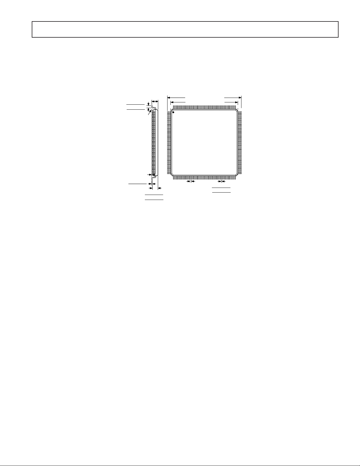
0.75 (0.030)
0.60 (0.024)
0.45 (0.018)
SEATING
PLANE
OUTLINE DIMENSIONS
Dimensions shown in mm and (inches).
184-Lead Plastic LQFP
(ST-184)
1.60 (0.063)
MAX
186
1
22.00 (0.866) BSC SQ
20.00 (0.787) BSC SQ
PIN 1
TOP VIEW
(PINS DOWN)
AD8151
139
138
0.08 (0.003)
0.15 (0.006)
0.05 (0.002)
1.45 (0.057)
1.40 (0.053)
1.35 (0.048)
CONTROLLING DIMENSIONS ARE IN MILLIMETERS
46
47
0.40 (0.016)
BSC
0.23 (0.009)
0.18 (0.007)
0.13 (0.005)
93
92
REV. 0
–35–

C02169–1.5–4/01(0)
–36–
PRINTED IN U.S.A.
 Loading...