

Low Cost, Low Power 12-Bit
FEATURES
Fully differential
Extremely low power with power-down feature
2.6 mA quiescent supply current @ 5 V
450 µA in power-down mode @ 5 V
High speed
110 MHz large signal 3 dB bandwidth @ G = 1
450 V/µs slew rate
12-bit SFDR performance @ 500 kHz
Fast settling time: 100 ns to 0.02%
Low input offset voltage: ±2.6 mV max
Low input offset current: 0.45 µA max
Differential input and output
Differential-to-differential or single-ended-to-differential
operation
Rail-to-rail output
Adjustable output common-mode voltage
Externally adjustable gain
Wide supply voltage range: 2.7 V to 12 V
Available in small SOIC package
APPLICATIONS
12-bit ADC drivers
Portable instrumentation
Battery-powered applications
Single-ended-to-differential converters
Differential active filters
Video amplifiers
Level shifters
GENERAL DESCRIPTON
Differential ADC Driver
AD8137
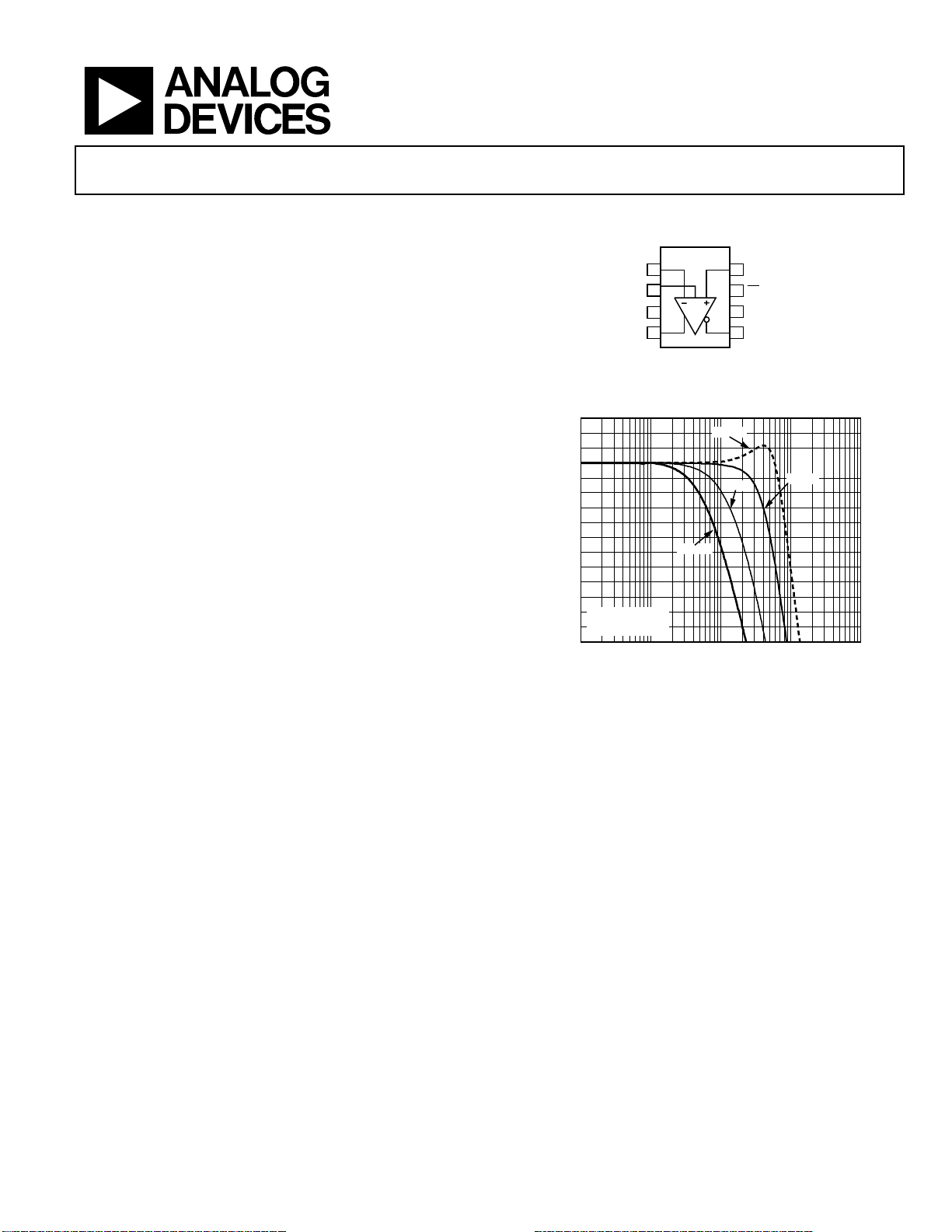
FUNCTIONAL BLOCK DIAGRAM
AD8137
–IN
1
2
V
OCM
3
V
S+
+OUT
4
Figure 1.
3
2
1
0
–1
–2
–3
–4
–5
–6
–7
–8
–9
–10
RG= 1kΩ
NORMALIZED CLOSED-LOOP GAIN (dB)
–11
–12
= 0.1V p-p
V
O, dm
0.1 1 10 100 1000
Figure 2. Small Signal Response for Various Gains
G = 10
FREQUENCY (MHz)
G = 1
G = 5
+IN
8
PD
7
6
V
S–
–OUT
5
04771-0-001
G = 2
04771-0-002
The AD8137 is a low cost differential driver with a rail-to-rail
output that is ideal for driving 12-bit ADCs in systems that are
sensitive to power and cost. The AD8137 is easy to apply, and its
internal common-mode feedback architecture allows its output
common-mode voltage to be controlled by the voltage applied
to one pin. The internal feedback loop also provides inherently
balanced outputs as well as suppression of even-order harmonic
distortion products. Fully differential and single-ended-todifferential gain configurations are easily realized by the
AD8137. External feedback networks consisting of four resistors
determine the amplifier’s closed-loop gain. The power-down
feature is beneficial in critical low power applications.
Rev. A
Information furnished by Analog Devices is believed to be accurate and reliable.
However, no responsibility is assumed by Analog Devices for its use, nor for any
infringements of patents or other rights of third parties that may result from its use.
Specifications subject to change without notice. No license is granted by implication
or otherwise under any patent or patent rights of Analog Devices. Trademarks and
registered trademarks are the property of their respective owners.
The AD8137 is manufactured on Analog Devices’ proprietary
second generation XFCB process, enabling it to achieve high
levels of performance with very low power consumption.
The AD8137 is available in the small 8-lead SOIC package and
3 mm × 3 mm LFCSP. It is rated to operate over the extended
industrial temperature range of −40°C to +125°C.
One Technology Way, P.O. Box 9106, Norwood, MA 02062-9106, U.S.A.
Tel: 781.329.4700
Fax: 781.326.8703 © 2004 Analog Devices, Inc. All rights reserved.
www.analog.com

AD8137
TABLE OF CONTENTS
Specifications..................................................................................... 3
REVISION HISTORY
Absolute Maximum Ratings............................................................ 6
Thermal Resistance ...................................................................... 6
ESD Caution.................................................................................. 6
Pin Configuration and Function Descriptions............................. 7
Typical Performance Characteristics ............................................. 8
Theory of Operation ...................................................................... 17
Applications..................................................................................... 18
Analyzing a Typical Application with Matched RF and RG
Networks...................................................................................... 18
Estimating Noise, Gain, and Bandwith with Matched
Feedback Networks.................................................................... 18
Driving an ADC with Greater Than 12-Bit Performance..... 22
Outline Dimensions....................................................................... 24
Ordering Guide........................................................................... 24
8/04—Data Sheet Changed from a Rev. 0 to Rev. A.
Added 8-Lead LFCSP.........................................................Universal
Changes to Layout.............................................................. Universal
Changes to Product Title..................................................................1
Changes to Figure 1...........................................................................1
Changes to Specifications.................................................................3
Changes to Absolute Maximum Ratings ........................................6
Changes to Figure 4 and Figure 5....................................................7
Added Figure 6, Figure 20, Figure 23, Figure 35, Figure 48,
and Figure 58; Renumbered Successive Figures............................7
Changes to Figure 32...................................................................... 12
Changes to Figure 40...................................................................... 13
Changes to Figure 55...................................................................... 16
Changes to Table 7 and Figure 63................................................. 18
Changes to Equation 19................................................................. 19
Changes to Figure 64 and Figure 65............................................. 20
Changes to Figure 66...................................................................... 22
Added Driving an ADC with Greater Than 12-Bit
Performance Section...................................................................... 22
Changes to Ordering Guide.......................................................... 24
Updated Outline Dimensions....................................................... 24
5/04—Revision 0: Initial Version
Rev. A | Page 2 of 24

AD8137
SPECIFICATIONS
Table 1. VS = ±5 V, V
Parameter Conditions Min Typ Max Unit
DIFFERENTIAL INPUT PERFORMANCE
DYNAMIC PERFORMANCE
−3 dB Small Signal Bandwidth V
−3 dB Large Signal Bandwidth V
Slew Rate V
Settling Time to 0.02% V
Overdrive Recovery Time G = 2, V
NOISE/HARMONIC PERFORMANCE
SFDR V
V
Input Voltage Noise f = 50 kHz to 1 MHz 8.25 nV/√Hz
Input Current Noise f = 50 kHz to 1 MHz 1 pA/√Hz
DC PERFORMANCE
Input Offset Voltage VIP = VIN = V
Input Offset Voltage Drift T
Input Bias Current T
Input Offset Current 0.1 0.45 µA
Open-Loop Gain 91 dB
INPUT CHARACTERISTICS
Input Common-Mode Voltage Range −4 +4 V
Input Resistance Differential 800 KΩ
Common-Mode 400 KΩ
Input Capacitance Common-Mode 1.8 pF
CMRR ∆V
OUTPUT CHARACTERISTICS
Output Voltage Swing Each Single-Ended Output, R
Output Current 20 mA
Output Balance Error f = 1 MHz −64 dB
V
to V
OCM
V
OCM
PERFORMANCE
O, cm
DYNAMIC PERFORMANCE
−3 dB Bandwidth V
Slew Rate V
Gain 0.992 1.000 1.008 V/V
V
INPUT CHARACTERISTICS
OCM
Input Voltage Range −4 +4 V
Input Resistance 35 kΩ
Input Offset Voltage −28 ±11 +28 mV
Input Voltage Noise f = 100 kHz to 1 MHz 18 nV/√Hz
Input Bias Current 0.3 1.1 µA
CMRR ∆V
POWER SUPPLY
Operating Range +2.7 ±6 V
Quiescent Current 3.2 3.6 mA
Quiescent Current, Disabled Power-Down = Low 750 900 µA
PSRR ∆VS = ±1 V 79 91 dB
PD PIN
Threshold Voltage VS− + 0.7 VS− + 1.7 V
Input Current Power-Down = High/Low 150/210 170/240 µA
OPERATING TEMPERATURE RANGE −40 +125 °C
= 0 V (@ 25°C, Diff. Gain = 1, R
OCM
O, dm
O, dm
O, dm
O, dm
O, dm
O, dm
MIN
MIN
ICM
O, cm
O, cm
O, dm
= RF = RG = 1 kΩ, unless otherwise noted, T
L, dm
MIN
to T
= −40°C to +125°C)
MAX
= 0.1 V p-p 64 76 MHz
= 2 V p-p 79 110 MHz
= 2 V Step 450 V/µs
= 3.5 V Step 100 ns
= 12 V p-p Triangle Wave 85 ns
I, dm
= 2 V p-p, fC = 500 kHz 90 dB
= 2 V p-p, fC = 2 MHz 76 dB
= 0 V
OCM
to T
3 µV/°C
MAX
to T
0.5 1 µA
MAX
−2.6 ±0.7 +2.6 mV
= ±1 V 66 79 dB
= 1 kΩ VS− + 0.55 VS+ − 0.55 V
L, dm
= 0.1 V p-p 58 MHz
= 0.5 V p-p 63 V/µs
/∆V
, ∆V
OCM
= ±0.5 V 62 75 dB
OCM
Rev. A | Page 3 of 24

AD8137
Table 2. VS = 5 V, V
Parameter Conditions Min Typ Max Unit
DIFFERENTIAL INPUT PERFORMANCE
DYNAMIC PERFORMANCE
−3 dB Small Signal Bandwidth V
−3 dB Large Signal Bandwidth V
Slew Rate V
Settling Time to 0.02% V
Overdrive Recovery Time G = 2, V
NOISE/HARMONIC PERFORMANCE
SFDR V
V
Input Voltage Noise f = 50 kHz to 1 MHz 8.25 nV/√Hz
Input Current Noise f = 50 kHz to 1 MHz 1 pA/√Hz
DC PERFORMANCE
Input Offset Voltage VIP = VIN = V
Input Offset Voltage Drift T
Input Bias Current T
Input Offset Current 0.1 0.45 µA
Open-Loop Gain 89 dB
INPUT CHARACTERISTICS
Input Common-Mode Voltage Range 1 4 V
Input Resistance Differential 800 KΩ
Common-Mode 400 KΩ
Input Capacitance Common-Mode 1.8 pF
CMRR ∆V
OUTPUT CHARACTERISTICS
Output Voltage Swing Each Single-Ended Output, R
Output Current 20 mA
Output Balance Error f = 1 MHz −64 dB
V
to V
OCM
V
OCM
PERFORMANCE
O, cm
DYNAMIC PERFORMANCE
−3 dB Bandwidth V
Slew Rate V
Gain 0.980 1.000 1.020 V/V
V
INPUT CHARACTERISTICS
OCM
Input Voltage Range 1 4 V
Input Resistance 35 kΩ
Input Offset Voltage −25 ±7.5 +25 mV
Input Voltage Noise f = 100 kHz to 5 MHz 18 nV/√Hz
Input Bias Current 0.25 0.9 µA
CMRR ∆V
POWER SUPPLY
Operating Range +2.7 ±6 V
Quiescent Current 2.6 2.8 mA
Quiescent Current, Disabled Power-Down = Low 450 600 µA
PSRR ∆VS = ±1 V 79 91 dB
PD PIN
Threshold Voltage VS− + 0.7 VS− + 1.5 V
Input Current Power-Down = High/Low 50/110 60/120 µA
OPERATING TEMPERATURE RANGE −40 +125 °C
= 2.5 V (@ 25°C, Diff. Gain = 1, R
OCM
O, dm
O, dm
O, dm
O, dm
O, dm
O, dm
MIN
MIN
ICM
O, cm
O, cm
O, dm
= RF = RG = 1 kΩ, unless otherwise noted, T
L, dm
MIN
to T
= −40°C to +125°C)
MAX
= 0.1 V p-p 63 75 MHz
= 2 V p-p 76 107 MHz
= 2 V Step 375 V/µs
= 3.5 V Step 110 ns
= 7 V p-p Triangle Wave 90 ns
I, dm
= 2 V p-p, fC = 500 kHz 89 dB
= 2 V p-p, fC = 2 MHz 73 dB
= 0 V
OCM
to T
3 µV/°C
MAX
to T
0.5 0.9 µA
MAX
−2.7 ±0.7 +2.7 mV
= ±1 V 64 90 dB
= 1 kΩ VS− + 0.45 VS+ − 0.45 V
L, dm
= 0.1 V p-p 60 MHz
= 0.5 V p-p 61 V/µs
/∆V
, ∆V
OCM
= ±0.5 V 62 75 dB
OCM
Rev. A | Page 4 of 24

AD8137
Table 3. VS = 3 V, V
Parameter Conditions Min Typ Max Unit
DIFFERENTIAL INPUT PERFORMANCE
DYNAMIC PERFORMANCE
−3 dB Small Signal Bandwidth V
−3 dB Large Signal Bandwidth V
Slew Rate V
Settling Time to 0.02% V
Overdrive Recovery Time G = 2, V
NOISE/HARMONIC PERFORMANCE
SFDR V
V
Input Voltage Noise f = 50 kHz to 1 MHz 8.25 nV/√Hz
Input Current Noise f = 50 kHz to 1 MHz 1 pA/√Hz
DC PERFORMANCE
Input Offset Voltage VIP = VIN = V
Input Offset Voltage Drift T
Input Bias Current T
Input Offset Current 0.1 0.4 µA
Open-Loop Gain 87 dB
INPUT CHARACTERISTICS
Input Common-Mode Voltage Range 1 2 V
Input Resistance Differential 800 MΩ
Common-Mode 400 MΩ
Input Capacitance Common-Mode 1.8 pF
CMRR ∆V
OUTPUT CHARACTERISTICS
Output Voltage Swing Each Single-Ended Output, R
Output Current 20 mA
Output Balance Error f = 1 MHz −64 dB
V
to V
OCM
V
OCM
PERFORMANCE
O, cm
DYNAMIC PERFORMANCE
−3 dB Bandwidth V
Slew Rate V
Gain 0.96 1.00 1.04 V/V
V
INPUT CHARACTERISTICS
OCM
Input Voltage Range 1.0 2.0 V
Input Resistance 35 kΩ
Input Offset Voltage −25 ±5.5 +25 mV
Input Voltage Noise f = 100 kHz to 5 MHz 18 nV/√Hz
Input Bias Current 0.3 0.7 µA
CMRR ∆V
POWER SUPPLY
Operating Range +2.7 ±6 V
Quiescent Current 2.3 2.5 mA
Quiescent Current, Disabled Power-Down = Low 345 460 µA
PSRR ∆VS = ±1 V 78 90 dB
PD PIN
Threshold Voltage VS− + 0.7 VS− + 1.5 V
Input Current Power-Down = High/Low 8/65 10/70 µA
OPERATING TEMPERATURE RANGE −40 +125 °C
= 1.5 V (@ 25°C, Diff. Gain = 1, R
OCM
O, dm
O, dm
O, dm
O, dm
O, dm
O, dm
MIN
MIN
O, cm
O, cm
= RF = RG = 1 kΩ, unless otherwise noted, T
L, dm
MIN
to T
= −40°C to +125°C)
MAX
= 0.1 V p-p 61 73 MHz
= 2 V p-p 62 93 MHz
= 2 V Step 340 V/µs
= 3.5 V Step 110 ns
= 5 V p-p Triangle Wave 100 ns
I, dm
= 2 V p-p, fC = 500 kHz 89 dB
= 2 V p-p, fC = 2 MHz 71 dB
= 0 V
OCM
to T
3 µV/°C
MAX
to T
0.5 0.9 µA
MAX
= ±1 V 64 80 dB
ICM
= 1 kΩ VS− + 0.37 VS+ − 0.37 V
L, dm
−2.75 ±0.7 +2.75 mV
= 0.1 V p-p 61 MHz
= 0.5 V p-p 59 V/µs
/∆V
, ∆V
O, dm
OCM
= ±0.5 V 62 74 dB
OCM
Rev. A | Page 5 of 24
AD8137
ABSOLUTE MAXIMUM RATINGS
Table 4.
Parameter Rating
Supply Voltage 12 V
V
OCM
VS+ to VS−
Power Dissipation See Figure 3
Input Common-Mode Voltage VS+ to VS−
Storage Temperature −65°C to +125°C
Operating Temperature Range −40°C to +125°C
Lead Temperature Range
300°C
(Soldering 10 sec)
Junction Temperature 150°C
Stresses above those listed under Absolute Maximum Ratings
may cause permanent damage to the device. This is a stress
rating only and functional operation of the device at these or
any other conditions above those indicated in the operational
section of this specification is not implied. Exposure to absolute
maximum rating conditions for extended periods may affect
device reliability.
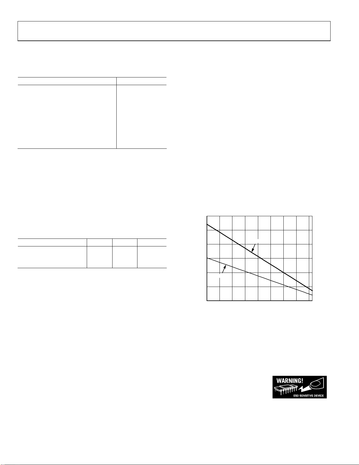
THERMAL RESISTANCE
θJA is specified for the worst-case conditions, i.e., θJA is specified
for the device soldered in a circuit board in still air.
Table 5. Thermal Resistance
Package Type θJA θ
SOIC-8/2-Layer 157 56 °C/W
SOIC-8/4-Layer 125 56 °C/W
LFCSP/4-Layer 70 56 °C/W
Maximum Power Dissipation
The maximum safe power dissipation in the AD8137 package is
limited by the associated rise in junction temperature (T
the die. At approximately 150°C, which is the glass transition
temperature, the plastic will change its properties. Even temporarily exceeding this temperature limit may change the stresses
that the package exerts on the die, permanently shifting the
parametric performance of the AD8137. Exceeding a junction
temperature of 175°C for an extended period of time can result
in changes in the silicon devices potentially causing failure.
Unit
JC
) on
J
The power dissipated in the package (P
quiescent power dissipation and the power dissipated in the
package due to the load drive for all outputs. The quiescent
power is the voltage between the supply pins (V
quiescent current (I
and common-mode currents flowing to the load, as well as
currents flowing through the external feedback networks and
the internal common-mode feedback loop. The internal resistor
tap used in the common-mode feedback loop places a 1 kΩ
differential load on the output. RMS output voltages should be
considered when dealing with ac signals.
Airflow reduces θ
the package leads from metal traces, through holes, ground, and
power planes will reduce the θ
Figure 3 shows the maximum safe power dissipation in the
package versus the ambient temperature for the SOIC-8
(125°C/W) and LFCSP (θ
standard 4-layer board. θ
3.0
2.5
2.0
1.5
1.0
0.5
MAXIMUM POWER DISSIPATION (W)
0
–40 –20–10–30 0 10 20 30 40 50 60 70 80 90 100110120
Figure 3. Maximum Power Dissipation vs. Temperature for a 4-Layer Board
) is the sum of the
D
) times the
S
). The load current consists of differential
S
. Als o, more metal dire ctly in contact with
JA
.
JA
= 70°C/W) package on a JEDEC
JA
values are approximations.
JA
LFCSP
SOIC-8
AMBIENT TEMPERATURE (°C)
04771-0-022
ESD CAUTION
ESD (electrostatic discharge) sensitive device. Electrostatic charges as high as 4000 V readily accumulate on the
human body and test equipment and can discharge without detection. Although this product features proprietary ESD protection circuitry, permanent damage may occur on devices subjected to high energy electrostatic
discharges. Therefore, proper ESD precautions are recommended to avoid performance degradation or loss of
functionality.
Rev. A | Page 6 of 24
AD8137
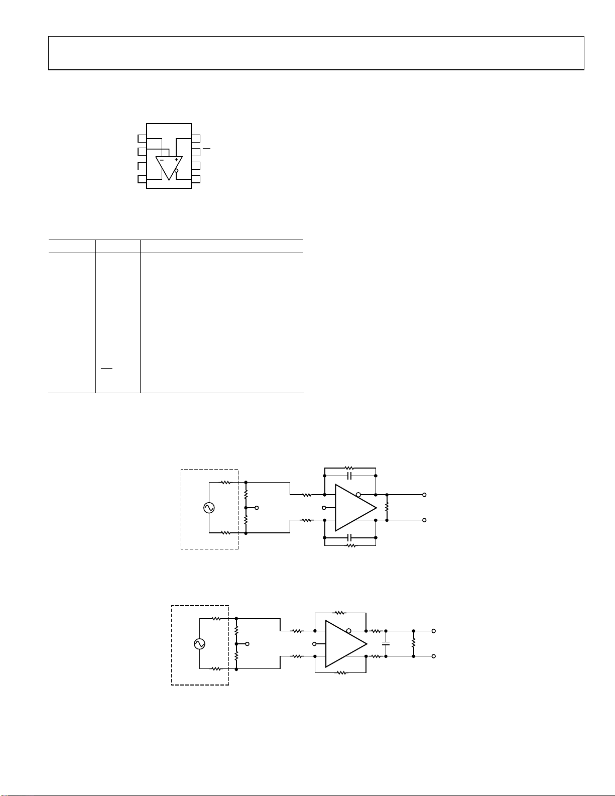
PIN CONFIGURATION AND FUNCTION DESCRIPTIONS
AD8137
–IN
V
OCM
V
+OUT
1
2
3
S+
4
+IN
8
PD
7
V
6
S–
–OUT
5
04771-0-001
Figure 4. Pin Configuration
Table 6. Pin Function Descriptions
Pin No. Name Description
1 −IN Inverting Input.
2 V
OCM
An internal feedback loop drives the
output common-mode voltage to be
equal to the voltage applied to the V
OCM
pin, provided the amplifier’s operation
remains linear.
3 VS+ Positive Power Supply Voltage.
4 +OUT Positive Side of the Differential Output.
5 −OUT Negative Side of the Differential Output.
6 VS− Negative Power Supply Voltage.
7
PD
Power Down.
8 +IN Noninverting Input.
R
F
V
TEST
TEST
SIGNAL
SOURCE
50Ω
50Ω
52.3Ω
MIDSUPPLY
52.3Ω
RG= 1kΩ
V
OCM
RG= 1kΩ
C
F
+
AD8137
–
C
F
R
F
R
L, dm
1kΩ V
–
+
O, dm
04771-0-023
Figure 5. Basic Test Circuit
V
TEST
TEST
SIGNAL
SOURCE
50Ω
50Ω
52.3Ω
MIDSUPPLY
52.3Ω
RG= 1kΩ
V
RG= 1kΩ
Figure 6. Capacitive Load Test Circuit, G = 1
OCM
RF= 1kΩ
+
AD8137
–
= 1kΩ
R
F
R
S
C
L, dm
R
S
–
R
L, dmVO, dm
+
04771-0-062
Rev. A | Page 7 of 24
AD8137
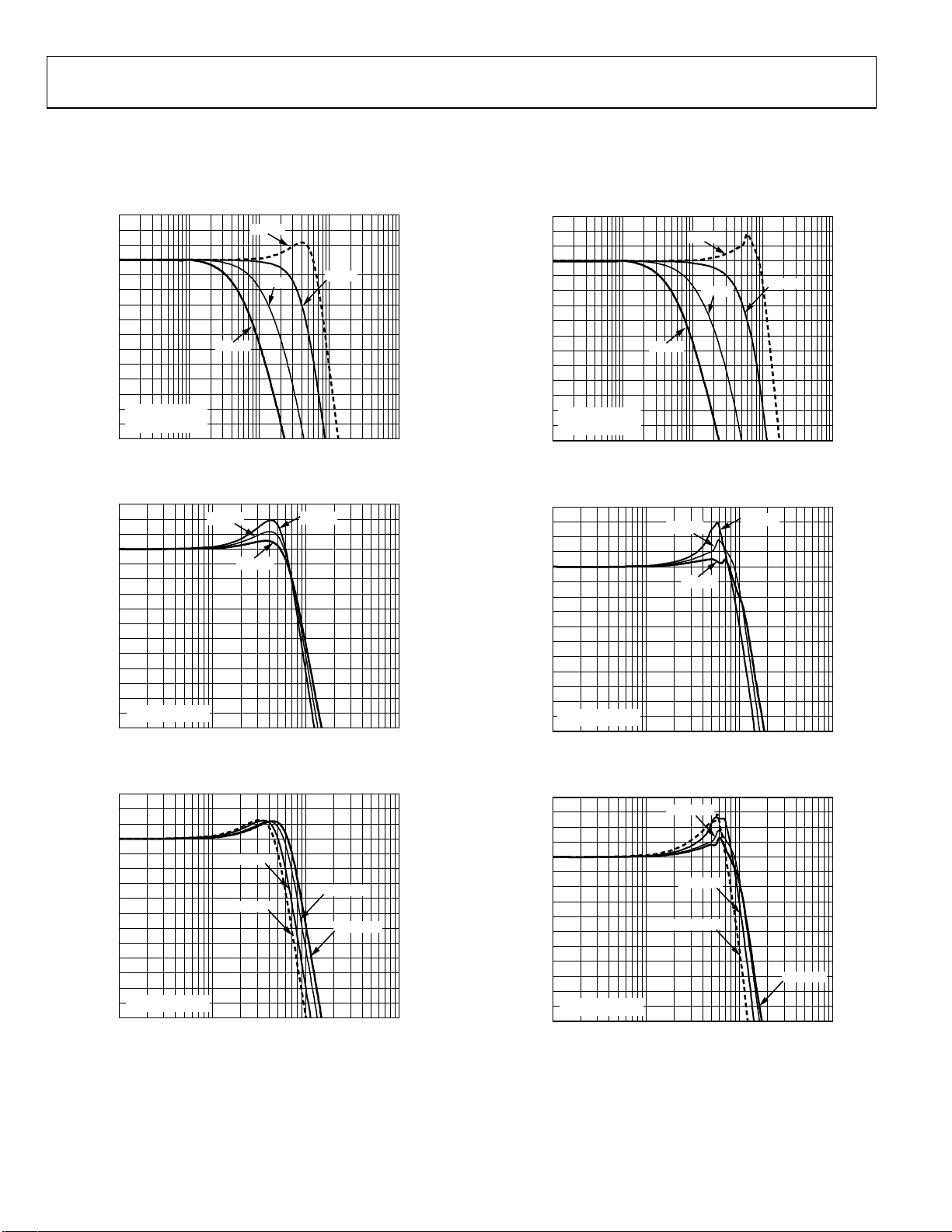
TYPICAL PERFORMANCE CHARACTERISTICS
Unless otherwise noted, Diff. Gain = 1, RG = RF = R
for the definition of terms.
3
2
1
0
–1
–2
–3
–4
–5
–6
–7
–8
–9
–10
RG= 1kΩ
NORMALIZED CLOSED-LOOP GAIN (dB)
–11
–12
= 0.1V p-p
V
O, dm
0.1 1 10 100 1000
Figure 7. Small Signal Frequency Response for Various Gains
3
2
1
0
–1
–2
–3
–4
–5
–6
–7
–8
CLOSED-LOOP GAIN (dB)
–9
–10
–11
V
= 0.1V p-p
O, dm
–12
1 10 100 1000
Figure 8. Small Signal Frequency Response for Various Power Supplies
3
2
1
0
–1
–2
–3
–4
–5
–6
–7
–8
CLOSED-LOOP GAIN (dB)
–9
–10
–11
V
= 0.1V p-p
O, dm
–12
1 10 100 1000
Figure 9. Small Signal Frequency Response at Various Temperatures
G = 1
G = 5
G = 10
FREQUENCY (MHz)
VS = +5
VS = ±5
FREQUENCY (MHz)
T = +85°C
T = +125°C
FREQUENCY (MHz)
G = 2
VS = +3
T = +25°C
= 1 kΩ, VS = 5 V, TA = 25°C, V
L, dm
04771-0-002
04771-0-003
T = –40°C
04771-0-006
= 2.5V. Refer to the basic test circuit in Figure 5
OCM
3
2
1
0
–1
–2
–3
–4
–5
–6
–7
–8
–9
–10
NORMALIZED CLOSED-LOOP GAIN (dB)
RG= 1kΩ
–11
–12
= 2.0V p-p
V
O, dm
0.1 1 10 100 1000
G = 1
G = 5
G = 10
FREQUENCY (MHz)
G = 2
Figure 10. Large Signal Frequency Response for Various Gains
4
3
2
1
0
–1
–2
–3
–4
–5
–6
–7
CLOSED-LOOP GAIN (dB)
–8
–9
–10
V
= 2.0V p-p
O, dm
–11
1 10 100 1000
VS = +5
VS = ±5
FREQUENCY (MHz)
VS = +3
Figure 11. Large Signal Frequency Response for Various Power Supplies
4
3
2
1
0
–1
–2
–3
–4
–5
–6
–7
CLOSED-LOOP GAIN (dB)
–8
–9
–10
V
= 2.0V p-p
O, dm
–11
1 10 100 1000
T = +25°C
T = +85°C
T = +125°C
T = –40°C
FREQUENCY (MHz)
Figure 12. Large Signal Frequency Response at Various Temperatures
04771-0-004
04771-0-005
04771-0-007
Rev. A | Page 8 of 24

AD8137
3
2
1
0
–1
–2
–3
–4
–5
–6
–7
–8
CLOSED-LOOP GAIN (dB)
–9
–10
–11
V
O, dm
–12
1 10 100 1000
= 0.1V p-p
R
= 1kΩ
L, dm
R
= 2kΩ
L, dm
FREQUENCY (MHz)
R
L, dm
= 500Ω
Figure 13. Small Signal Frequency Response for Various Loads
3
2
1
0
–1
–2
–3
–4
–5
–6
–7
–8
CLOSED-LOOP GAIN (dB)
–9
–10
–11
V
= 0.1V p-p
O, dm
–12
1 10 100 1000
CF= 2pF
FREQUENCY (MHz)
CF= 0pF
CF= 1pF
Figure 14. Small Signal Frequency Response for Various C
2
1
0
–1
–2
–3
–4
–5
–6
–7
–8
–9
CLOSED-LOOP GAIN (dB)
–10
–11
–12
V
O, dm
–13
1 10 100 1000
= 0.1V p-p
V
= 4V
OCM
V
= 1V
OCM
FREQUENCY (MHz)
V
= 2.5V
OCM
Figure 15. Small Signal Frequency Response at Various V
OCM
04771-0-041
04771-0-008
F
04771-0-042
3
2
1
0
–1
–2
–3
–4
–5
–6
–7
–8
CLOSED-LOOP GAIN (dB)
–9
–10
–11
V
= 2V p-p
O, dm
–12
1 10 100 1000
R
= 2kΩ
L, dm
= 1kΩ
R
L, dm
FREQUENCY (MHz)
R
Figure 16. Large Signal Frequency Response for Various Loads
3
2
1
0
–1
–2
–3
–4
–5
–6
–7
–8
CLOSED-LOOP GAIN (dB)
–9
–10
–11
V
= 2.0V p-p
O, dm
–12
1 10 100 1000
CF= 2pF
FREQUENCY (MHz)
CF= 0pF
CF= 1pF
Figure 17. Large Signal Frequency Response for Various C
3
2
1
0
–1
–2
–3
–4
–5
–6
–7
–8
CLOSED-LOOP GAIN (dB)
–9
–10
–11
–12
1 10 100 1000
0.5V p-p
0.1V p-p
FREQUENCY (MHz)
Figure 18. Frequency Response for Various Output Amplitudes
L, dm
2V p-p
1V p-p
= 500Ω
04771-0-043
04771-0-009
F
04771-0-044
Rev. A | Page 9 of 24

AD8137
4
3
2
1
0
–1
–2
–3
–4
–5
–6
CLOSED-LOOP GAIN (dB)
–7
–8
G= 1
–9
V
=±5V
S
–10
–11
= 0.1V p-p
V
O, dm
1 10 100 1000
RF = 2k
Ω
RF = 1k
Ω
FREQUENCY (MHz)
Figure 19. Small Signal Frequency Response for Various R
–65
G = 1
= 2V p-p
V
O, dm
–70
–75
–80
–85
–90
DISTORTION (dBc)
–95
–100
–105
0.1 1 10
VS = +3V
VS = ±5V
FREQUENCY (MHz)
Figure 20. Second Harmonic Distortion vs. Frequency and Supply Voltage
–50
FC = 500kHz
–55
SECOND HARMONIC SOLID LINE
THIRD HARMONIC DASHED LINE
–60
–65
–70
–75
–80
DISTORTION (dBc)
–85
–90
–95
–100
0.25 1.25 2.25 3.25 4.25 5.25 7.25 8.256.25 9.25
VS = +3V
V
O, dm
VS = +3V
(V p-p)
Figure 21. Harmonic Distortion vs. Output Amplitude and Supply, F
VS = +5V
VS = +5V
VS = +5V
R
= 500
F
Ω
F
= 500 kHz
C
04771-0-037
04771-0-045
04771-0-027
4
3
2
1
0
–1
–2
–3
–4
–5
–6
CLOSED-LOOP GAIN (dB)
–7
–8
–9
G = 1
–10
–11
= 2V p-p
V
O, dm
1 10 100 1000
RF = 2k
Ω
RF = 1k
Ω
FREQUENCY (MHz)
R
= 500
F
Figure 22. Large Signal Frequency Response for Various R
–40
G = 1
= 2V p-p
V
O, dm
–50
–60
–70
–80
DISTORTION (dBc)
–90
–100
–110
0.1 1 10
VS = +3V
VS = +5V
VS =±5V
FREQUENCY (MHz)
Figure 23. Third Harmonic Distortion vs. Frequency and Supply Voltage
–50
–55
–60
–65
–70
–75
–80
DISTORTION (dBc)
–85
–90
–95
–100
0.25 1.25 2.25 3.25 4.25 5.25 7.25 8.256.25 9.25
VS = +3V
VS = +3V
VS = +5V
FC = 2MHz
SECONDHARMONIC SOLIDLINE
THIRD HARMONIC DASHED LINE
V
(V p-p)
O, dm
VS = +5V
Figure 24. Harmonic Distortion vs. Output Amplitude and Supply, F
Ω
F
= 2 MHz
C
04771-0-036
04771-0-063
04771-0-026
Rev. A | Page 10 of 24

AD8137
–40
–50
V
O, dm
= 2V p-p
–40
–50
V
O, dm
= 2V p-p
–60
R
= 200Ω
–70
–80
DISTORTION (dBc)
–90
–100
–110
0.1 1 10
L, dm
R
= 500Ω
L, dm
FREQUENCY (MHz)
R
L, dm
Figure 25. Second Harmonic Distortion at Various Loads
–40
V
= 2V p-p
O, dm
= 1kΩ
R
G
–50
–60
–70
–80
DISTORTION (dBc)
–90
–100
–110
0.1 1 10
FREQUENCY (MHz)
G = 5
Figure 26. Second Harmonic Distortion at Various Gains
–40
V
= 2V p-p
O, dm
G = 1
–50
–60
= 500Ω
–70
–80
DISTORTION (dBc)
–90
–100
–110
0.1 1 10
R
F
RF = 1kΩ
FREQUENCY (MHz)
R
= 2kΩ
F
Figure 27. Second Harmonic Distortion at Various R
= 1kΩ
G = 2
G = 1
F
04771-0-032
04771-0-034
04771-0-030
–60
= 200Ω
R
–70
–80
DISTORTION (dBc)
–90
–100
–110
0.1 1 10
L, dm
R
L, dm
R
= 500Ω
L, dm
FREQUENCY (MHz)
= 1kΩ
Figure 28. Third Harmonic Distortion at Various Loads
–40
V
= 2V p-p
O, dm
= 1kΩ
R
G
–50
–60
–70
–80
DISTORTION (dBc)
–90
–100
–110
0.1 1 10
FREQUENCY (MHz)
G = 5
G = 2
G = 1
Figure 29. Third Harmonic Distortion at Various Gains
–40
V
= 2V p-p
O, dm
G = 1
–50
–60
–70
–80
DISTORTION (dBc)
–90
–100
–110
= 500Ω
R
F
= 2kΩ
R
RF = 1kΩ
0.1 1 10
F
FREQUENCY (MHz)
Figure 30. Third Harmonic Distortion at Various R
04771-0-033
04771-0-035
04771-0-031
F
Rev. A | Page 11 of 24

AD8137
–50
–60
FC = 500kHz
= 2V p-p
V
O, dm
SECOND HARMONIC SOLID LINE
THIRD HARMONIC DASHED LINE
–50
–60
FC = 500kHz
V
= 2V p-p
O, dm
SECOND HARMONIC SOLID LINE
THIRD HARMONIC DASHED LINE
–70
–80
–90
DISTORTION (dBc)
–100
–110
0.5 1.0 1.5 2.52.0 3.5 4.03.0 4.5
Figure 31. Harmonic Distortion vs. V
100
10
INPUT VOLTAGE NOISE (nV/√Hz)
1
10 100 1k 10k 100k 1M 10M 100M
V
(V)
OCM
FREQUENCY (Hz)
, VS = +5 V
OCM
Figure 32. Input Voltage Noise vs. Frequency
20
V
= 0.2V p-p
IN, cm
10
INPUT CMRR =
0
–10
–20
–30
CMRR (dB)
–40
–50
–60
–70
–80
1 10 100
∆
V
∆
V
O, cm/
IN, cm
FREQUENCY (MHz)
Figure 33. CMRR v s. Frequen cy
–70
–80
–90
DISTORTION (dBc)
–100
04771-0-028
04771-0-046
04771-0-013
–110
0.5 0.7 0.9 1.31.1 1.5 1.7 2.32.11.9 2.5
Figure 34. Harmonic Distortion vs. V
1000
100
NOISE (nV/√Hz)
10
OCM
V
1
10 100 1k 10k 100k 1M 10M 100M
Figure 35. V
–10
V
= 0.2V p-p
O, cm
V
CMRR =∆V
OCM
–20
–30
–40
CMRR (dB)
–50
OCM
V
–60
–70
–80
1 10 100
Figure 36. V
V
(V)
OCM
OCM
FREQUENCY (Hz)
Voltage Noise vs. Frequency
OCM
∆
V
O, dm/
OCM
FREQUENCY (MHz)
CMRR vs. Frequency
OCM
, VS = +3 V
04771-0-029
04771-0-047
04771-0-012
Rev. A | Page 12 of 24

AD8137
8
G = 2
6
4
INPUT
×
2
OUTPUT
2.0
1.5
1.0
V
O, dm
INPUT
CF = 0pF
V
O, dm
= 3.5V p-p
2
0
VOLTAGE (V)
–2
–4
–6
–8
TIME (ns)
250ns/DIV
04771-0-016
Figure 37. Overdrive Recovery
100
75
50
(mV)
O, dm
V
CF = 0pF
25
0
–25
–50
–75
–100
C
V
= 1pF
F
O, dm
= 100mV p-p
TIME (ns)
10ns/DIV
04771-0-015
Figure 38. Small Signal Transient Response for Various Feedback Capacitances
100
75
50
RS = 111, CL= 5pF
RS = 60.4, CL= 15pF
(V)
O, dm
V
25
0
–25
–50
0.5
0
–0.5
AMPLITUDE (V)
–1.0
–1.5
–2.0
T
SETTLE
TIME (ns)
ERROR = V
= 110ns
O, dm
- INPUT
50ns/DIV
ERROR (V) 1DIV = 0.02%
04771-0-040
Figure 40. Settling Time (0.02%)
1.5
(V)
O, dm
V
1.0
0.5
–0.5
–1.0
–1.5
CF = 0pF
C
F
C
F
C
= 1pF
F
0
= 1pF
= 0pF
TIME (ns)
2V p-p
1V p-p
20ns/DIV
04771-0-014
Figure 41. Large Signal Transient Response for Various Feedback Capacitances
1.5
RS = 111, CL= 5pF
1.0
0.5
(V)
O, dm
V
0
–0.5
RS = 60.4, CL= 15pF
–75
–100
TIME (ns)
20ns/DIV
Figure 39. Small Signal Transient Response for Various Capacitive Loads
04771-0-039
Rev. A | Page 13 of 24
–1.0
–1.5
TIME (ns)
20ns/DIV
Figure 42. Large Signal Transient Response for Various Capacitive Loads
04771-0-038

AD8137
–5
–15
–25
–35
–45
PSRR (dB)
–55
–65
–75
–85
0.1 1 10 100
1
0
–1
–2
–3
–4
–5
–6
–7
–8
–9
–10
CLOSED-LOOP GAIN (dB)
–11
–12
–13
–14
1 10 100 1000
Figure 44. V
700
600
500
400
300
200
100
0
–100
–200
–300
–400
–500
–600
SINGLE-ENDED OUTPUT SWING FROM RAIL (mV)
–700
200 1k 10k
PSRR =∆V
O, dm/
∆
V
–PSRR
S
+PSRR
FREQUENCY (MHz)
Figure 43. PSRR vs. Frequency
VS = +5
VS = +3
V
= 0.1V p-p
O, dm
FREQUENCY (MHz)
Small Signal Frequency Response for Various Supply Voltages
OCM
VS+– V
OP
V
= +5V
S
VS = +3V
VON– V
RESISTIVE LOAD (Ω)
S–
VS =±5
Figure 45. Output Saturation Voltage vs. Output Load
04771-0-011
04771-0-010
04771-0-049
1000
100
)
Ω
10
1
OUTPUT IMPEDANCE (
0.1
0.01
0.01 1001010.1
FREQUENCY (MHz)
Figure 46. Single-Ended Output Impedance vs. Frequency
4.0
3.5
3.0
(V)
2.5
O, cm
V
2.0
1.5
1.0
Figure 47. V
350
345
340
335
330
SWING FROM RAIL (mV)
OP
V
325
320
–40 –20 0 20 40 60 80 100 120
OCM
TEMPERATURE (°C)
2V p-p
1V p-p
TIME (ns)
Large Signal Transient Response
VON– VS–
VS+ – V
OP
Figure 48. Output Saturation Voltage vs. Temperature
20ns/DIV
–300
–305
–310
–315
–320
–325
–330
04771-0-061
04771-0-050
SWING FROM RAIL (mV)
ON
V
04771-0-065
Rev. A | Page 14 of 24

AD8137
0.3
15
2.60
0.2
0.1
(mV)
0
OS, dm
V
–0.1
–0.2
–0.3
–40 –20 0 20 40 60 80 100 120
V
OS, cm
TEMPERATURE (°C)
V
OS, dm
Figure 49. Offset Voltage vs. Temperature
1.2
1.0
0.8
A)
µ
0.6
0.4
0.2
0
INPUT BIAS CURRENT (
–0.2
–0.4
0.50 1.50 2.50 3.50 4.50
V
(V)
ACM
Figure 50. Input Bias Current vs. Input Common-Mode Voltage, V
0.40
10
5
0
5
10
–15
ACM
3
(mV)
OS, cm
V
04771-0-052
04771-0-059
2.55
2.50
2.45
2.40
SUPPLY CURRENT (mA)
2.35
2.30
–40 0 20–20 40 80 10060 120
TEMPERATURE (°C)
Figure 52. Supply Current vs. Temperature
70
50
30
A)
10
µ
(
OCM
–10
V
I
–30
–50
–70
0 0.5 1.0 1.5 2.0 2.5 3.0 3.5 4.0 4.5 5.0
Figure 53. V
–0.1
OCM
V
(V)
OCM
Bias Current vs. V
Input Voltage
OCM
04771-0-051
04771-0-056
0.35
0.30
(µA)
0.25
BIAS
I
0.20
0.15
0.10
–40 –20 0 20 40 60 80 100 120
I
BIAS
TEMPERATURE (°C)
Figure 51. Input Bias and Offset Current vs. Temperature
2
1
0
(nA)
I
OS
OS
I
–1
–2
04771-0-053
–3
–0.2
–0.3
CURRENT (µA)
OCM
V
–0.4
–0.5
–40 –20 0 20 40 60 80 100 120
Figure 54. V
TEMPERATURE (°C)
Bias Current vs. Temperature
OCM
04771-0-054
Rev. A | Page 15 of 24

AD8137
5
4
3
2
1
0
O, cm
V
–1
–2
–3
–4
–5
–5 –4 –3 –2 –1 432105
40
20
0
–20
–40
–60
PD CURRENT (µA)
–80
–100
–120
0 0.5 1.0 1.5 2.0 2.5 3.0 3.5 4.0 4.5 5.0
3
2
1
Figure 55. V
Figure 56.
VS =±5V
V
OCM
vs. V
O, cm
PD
Input Voltage
OCM
PD VOLTAGE (V)
Current vs. PD Volta ge
IS+
VS = +5V
VS = +3V
04771-0-060
04771-0-057
1.5
1.0
0.5
–0.5
SUPPLY CURRENT (mA)
–1.0
–1.5
3.6
3.2
2.8
2.4
2.0
1.6
1.2
SUPPLY CURRENT (mA)
0.8
0.4
3.4
3.0
2.6
2.2
V
O, dm
0
–0.5V
–2.0V
PD
TIME (µs)
Figure 58. Power-Down Transient Response
PD (0.8V TO 1.5V)
0
TIME (ns)
Figure 59. Power-Down Turn-O n Time
PD (1.5V TO 0.8V)
VS = ±2.5V
G = 1 (R
= RG = 1kΩ)
F
= 1kΩ
R
L, dm
INPUT = 1Vp-p @ 1MHz
2µs/DIV
100ns/DIV
04771-0-066
04771-0-024
0
–1
SUPPLY CURRENT (mA)
–2
–3
0 0.5 1.0 1.5 2.0 2.5 3.0 3.5 4.0 4.5 5.0
PD VOLTAGE (V)
Figure 57. Supply Current vs.
–
I
S
PD
Volta ge
04771-0-058
Rev. A | Page 16 of 24
1.8
1.4
SUPPLY CURRENT (mA)
1.0
0.6
0.2
TIME (ns)
Figure 60. Power-Down Turn-O ff Time
40ns/DIV
04771-0-025

AD8137
g
–
–
–
–
–
–
THEORY OF OPERATION
The AD8137 is a low power, low cost, fully differential voltage
feedback amplifier that features a rail-to-rail output stage,
common-mode circuitry with an internally derived commonmode reference voltage, and bias shutdown circuitry. The amplifier uses two feedback loops to separately control differential
and common-mode feedback. The differential gain is set with
external resistors as in a traditional amplifier while the output
common-mode voltage is set by an internal feedback loop,
controlled by an external V
input. This architecture makes it
OCM
easy to arbitrarily set the output common-mode voltage level
without affecting the differential gain of the amplifier.
V
OCM
A
CM
–OUT +IN
CP +OUT–IN CN
C
C
Figure 61. Block Diagram
C
C
04771-0-017
From Figure 61, the input transconductance stage is an
H-bridge whose output current is mirrored to high impedance
nodes CP and CN. The output section is traditional H-bridge
driven circuitry with common emitter devices driving nodes
+OUT and −OUT. The 3 dB point of the amplifier is defined as
m
C
2
C
is the transconductance of the input stage and CC is
where
BW×π=
g
m
the total capacitance on node CP/CN (capacitances CP and CN
are well matched). For the AD8137, the input stage g
~1 mA/V and the capacitance C
is 3.5 pF, setting the crossover
C
is
m
frequency of the amplifier at 41 MHz. This frequency generally
establishes an amplifier’s unity gain bandwidth, but with the
AD8137, the closed-loop bandwidth depends upon the
feedback resistor value as well (see Figure 19). The open-loop
gain and phase simulations are shown in Figure 62.
100
80
60
40
20
0
–20
–40
–60
–80
100
120
140
160
180
200
PHASE (DEGREES)
0.0001 0.010.001 0.1 1 10 100
OPEN-LOOP GAIN (dB)
FREQUENCY (MHz)
Figure 62. Open-Loop Gain and Phase
04771-0-021
In Figure 61, the common-mode feedback amplifier ACM
samples the output common-mode voltage, and by negative
feedback forces the output common-mode voltage to be equal
to the voltage applied to the V
input. In other words, the
OCM
feedback loop servos the output common-mode voltage to the
voltage applied to the V
sets the V
level to approximately midsupply, therefore, the
OCM
input. An internal bias generator
OCM
output common-mode voltage will be set to approximately
midsupply when the V
input is left floating. The source resis-
OCM
tance of the internal bias generator is large and can be overridden easily by an external voltage supplied by a source with a
relatively small output resistance. The V
input can be driven
OCM
to within approximately 1 V of the supply rails while maintaining linear operation in the common-mode feedback loop.
The common-mode feedback loop inside the AD8137 produces
outputs that are highly balanced over a wide frequency range
without the requirement of tightly matched external components because it forces the signal component of the output
common-mode voltage to be zeroed. The result is nearly
perfectly balanced differential outputs of identical amplitude
and exactly 180° apart in phase.
Rev. A | Page 17 of 24

AD8137
=
APPLICATIONS
ANALYZING A TYPICAL APPLICATION WITH
MATCHED R
Typical Connection and Definition of Terms
Figure 63 shows a typical connection for the AD8137, using
matched external RF/RG networks. The differential input
terminals of the AD8137, V
junctions. An external reference voltage applied to the V
terminal sets the output common-mode voltage. The two
output terminals, V
balanced fashion in response to an input signal.
AND RG NETWORKS
F
and VON, move in opposite directions in a
OP
R
V
G
V
IP
V
OCM
V
IN
AP
R
G
V
AN
and VAN, are used as summing
AP
C
F
R
F
V
+
AD8137
–
R
F
ON
R
L, dm
V
OP
V
–
O, dm
+
OCM
Output balance is measured by placing a well matched resistor
divider across the differential voltage outputs and comparing
the signal at the divider’s midpoint with the magnitude of the
differential output. By this definition, output balance is equal to
the magnitude of the change in output common-mode voltage
divided by the magnitude of the change in output differentialmode voltage:
BalanceOutput
V
∆
cmO
,
=
∆
(3)
V
dmO
,
The differential negative feedback drives the voltages at the summing junctions V
and VAP to be essentially equal to each other.
AN
VV
(4)
APAN
The common-mode feedback loop drives the output commonmode voltage, sampled at the midpoint of the two internal
common-mode tap resistors in Figure 61, to equal the voltage
set at the V
terminal. This ensures that
OCM
C
F
Figure 63. Typical Connection
04771-0-055
The differential output voltage is defined as
VVV −= (1)
dmO,
ONOP
Common-mode voltage is the average of two voltages. The
output common-mode voltage is defined as
VVV+
= (2)
,
cmO
ONOP
2
Output Balance
Output balance is a measure of how well VOP and VON are
matched in amplitude and how precisely they are 180 degrees
out of phase with each other. It is the internal common-mode
feedback loop that forces the signal component of the output
common-mode towards zero, resulting in the near perfectly
balanced differential outputs of identical amplitude and exactly
180 degrees out of phase. The output balance performance does
not require tightly matched external components, nor does it
require that the feedback factors of each loop be equal to each
other. Low frequency output balance is limited ultimately by the
mismatch of an on-chip voltage divider.
V
VV +=
OCMOP
, dmO
(5)
2
and
V
VV −=
OCMON
, dmO
(6)
2
ESTIMATING NOISE, GAIN, AND BANDWITH WITH
MATCHED FEEDBACK NETWORKS
Estimating Output Noise Voltage and Bandwidth
The total output noise is the root-sum-squared total of several
statistically independent sources. Since the sources are statistically independent, the contributions of each must be individually included in the root-sum-square calculation. Table 7 lists
recommended resistor values and estimates of bandwidth and
output differential voltage noise for various closed-loop gains.
For most applications, 1% resistors are sufficient.
Table 7. Recommended Values of Gain-Setting Resistors, and
Voltage Gain for Various Closed-Loop Gains
3 dB
Gain RG (Ω) RF (Ω)
Bandwidth (MHz)
1 1 k 1 k 72 18.6
2 1 k 2 k 40 28.9
5 1 k 5 k 12 60.1
10 1 k 10 k 6 112.0
The differential output voltage noise contains contributions
from the AD8137’s input voltage noise and input current noise
as well as those from the external feedback networks.
Total Output
Noise (nV/√Hz)
Rev. A | Page 18 of 24

AD8137
===
(
)
β−+β=
(
)
β+=
+
=
The contribution from the input voltage noise spectral density
is computed as
R
⎞
⎛
F
, or equivalently, vn/β (7)
+=
⎟
R
G
⎠
where
vVo_n 11
⎜
n
⎝
v
is defined as the input-referred differential voltage
n
noise. This equation is the same as that of traditional op amps.
The contribution from the input current noise of each input is
computed as
()
RiVo_n =2 (8)
n
F
where i
is defined as the input noise current of one input. Each
n
input needs to be treated separately since the two input currents
are statistically independent processes.
The contribution from each R
=
TRVo_n k43 (9)
G
G
R
⎛
⎞
F
⎜
⎟
R
G
⎝
⎠
is computed as
This result can be intuitively viewed as the thermal noise of
each R
multiplied by the magnitude of the differential gain.
G
This notation is consistent with conventional feedback analysis
and is very useful, particularly when the two feedback loops are
not matched.
Input Common-Mode Voltage
The linear range of the VAN and VAP terminals extends to within
approximately 1 V of either supply rail. Since V
essentially equal to each other, they are both equal to the amplifier’s input common-mode voltage. Their range is indicated in
the specifications tables as input common-mode range. The
voltage at V
can be expressed as
⎛
⎜
⎝
where V
fier input terminals.
Using the β notation, Equation (15) can be written as
G
≡β (14)
RRR+
F
G
and VAP are
AN
and VAP for the connection diagram in Figure 63
AN
VVV
ACMAPAN
R
F
×
RR
+
F
G
is the common-mode voltage present at the ampli-
ACM
)(
+
INIP
2
RVV
⎛
⎞
⎟
⎠
G
+
⎜
RR
+
F
⎝
G
⎞
(15)
V
×
⎟
OCM
⎠
The contribution from each R
TRVo_n k44 = (10)
F
is computed as
F
Voltage Gain
The behavior of the node voltages of the single-ended-todifferential output topology can be deduced from the signal
definitions and Figure 63. Referring to Figure 63, (C
setting V
= 0 one can write:
IN
VV −
−
IP
AP
=
R
G
==
VVV (12)
OPAPAN
VV
ONAP
(11)
R
F
R
⎡
⎢
⎣
⎤
G
⎥
+
RR
F
G
⎦
Solving the above two equations and setting V
gain relationship for V
VVV ==− (13)
ONOP
O, dm/Vi
dmO,
.
R
F
V
i
R
G
= 0) and
F
to Vi gives the
IP
An inverting configuration with the same gain magnitude can
be implemented by simply applying the input signal to V
setting V
V
IN, dm
= 0. For a balanced differential input, the gain from
IP
to V
is also equal to RF/RG, where V
O, dm
= VIP − VIN.
IN, dm
IN
and
Feedback Factor Notation
When working with differential drivers, it is convenient to introduce the feedback factor β, which is defined as
VVV
1 (16)
ICMOCMACM
or equivalently,
VVVV −
(17)
ICMOCMICMACM
where V
V
ICM
For proper operation, the voltages at V
is the common-mode voltage of the input signal, i.e.,
ICM
VV
INIP
≡
.
2
and VAP must stay
AN
within their respective linear ranges.
Calculating Input Impedance
The input impedance of the circuit in Figure 63 will depend on
whether the amplifier is being driven by a single-ended or a
differential signal source. For balanced differential input signals,
the differential input impedance (R
RR 2
(18)
dmIN,
G
For a single-ended signal (for example, when V
and the input signal drives V
R
=
R
IN
G
R
1
F
−
RR
+
G
), the input impedance becomes
IP
(19)
)(2
F
) is simply
IN, dm
is grounded,
IN
Rev. A | Page 19 of 24

AD8137
0
F
+2.5V
GND
–2.5V
0.1µF 0.1µF
1kΩ
V
OCM
V
IN
V
REFB
1kΩ 1kΩ
ACM WITH
V
= 0
REFB
2.5V
3
8
+
2
AD8137
1
–
6
1kΩ5V50Ω
5
4
+1.88V
+1.25VV
+0.63V
Figure 64. AD8137 Driving AD7450A, 12-Bit A/D Converter
The input impedance of a conventional inverting op amp
configuration is simply R
, but it is higher in Equation 19
G
because a fraction of the differential output voltage appears at
the summing junctions, V
bootstraps the voltage across the input resistor R
and VAP. This voltage partially
AN
, leading to the
G
increased input resistance.
Input Common-Mode Swing Considerations
In some single-ended-to-differential applications when using a
single-supply voltage, attention must be paid to the swing of the
input common-mode voltage, V
Consider the case in Figure 64, where V
about a baseline at ground and V
.
ACM
is 5 V p-p swinging
IN
is connected to ground.
REFB
The input signal to the AD8137 is originating from a source
with a very low output resistance.
The circuit has a differential gain of 1.0 and β = 0.5. V
ICM
has an
amplitude of 2.5 V p-p and is swinging about ground. Using the
results in Equation 16, the common-mode voltage at the AD8137’s
inputs, V
V. The maximum negative excursion of V
, is a 1.25 V p-p signal swinging about a baseline of 1.25
ACM
in this case is 0.63 V,
ACM
which exceeds the lower input common-mode voltage limit.
One way to avoid the input common-mode swing limitation is
to bias V
and V
IN
swinging about a baseline at 2.5 V, and V
low-Z 2.5 V source. V
is swinging about 2.5 V. Using the results in Equation 17, V
calculated to be equal to V
swings from 1.25 V to 3.75 V, which is well within the input
V
ICM
at midsupply. In this case, VIN is 5 V p-p
REF
is connected to a
REF
now has an amplitude of 2.5 V p-p and
ICM
because V
ICM
OCM
= V
. Therefore,
ICM
ACM
is
common-mode voltage limits of the AD8137. Another benefit
= V
= V
seen by this example is that since V
OCM
ACM
, no waste d
ICM
common-mode current flows. Figure 65 illustrates a way to
provide the low-Z bias voltage. For situations that do not
require a precise reference, a simple voltage divider will suffice
to develop the input voltage to the buffer.
1.0nF
VDD
VIN–
AD7450A
V
V TO 5V
0.1µF
10µF
VIN+
IN
GND V
0.1µF
1kΩ
V
OCM
1kΩ 1kΩ
0.1µF
+
REF
V
REFA
8
+
2
AD8137
1
–
ADR525A
2.5V SHUNT
REFERENCE
5V
1kΩ
3
4
6
5V
AD8031
2.5kΩ
04771-0-018
5
TO
AD7450A
V
REF
ADR525A
0.1µF
2.5V SHUNT
REFERENCE
+
–
50Ω
1.0nF
Figure 65. Low-Z Bias Source
Another way to avoid the input common-mode swing limitation is to use dual power supplies on the AD8137. In this case,
the biasing circuitry is not required.
Bandwidth Versus Closed-Loop Gain
The AD8137’s 3 dB bandwidth will decrease proportionally to
increasing closed-loop gain in the same way as a traditional
voltage feedback operational amplifier. For closed-loop gains
greater than 4, the bandwidth obtained for a specific gain can be
estimated as
R
G
=
Vf
dmO,dB
3
−
×
RR
+
G
)MHz72(,
(20)
or equivalently, β(72 MHz).
This estimate assumes a minimum 90 degree phase margin for
the amplifier loop, a condition approached for gains greater
than 4. Lower gains will show more bandwidth than predicted
by the equation due to the peaking produced by the lower phase
margin.
10kΩ
04771-0-019
Rev. A | Page 20 of 24

AD8137
Estimating DC Errors
Primary differential output offset errors in the AD8137 are due
to three major components: the input offset voltage, the offset
between the V
and VAP input currents interacting with the
AN
feedback network resistances, and the offset produced by the dc
voltage difference between the input and output common-mode
voltages in conjunction with matching errors in the feedback
network.
The first output error component is calculated as
+
RR
where V
⎛
=
VVo_e1 , or equivalently as V
⎜
IO
⎝
is the input offset voltage.
IO
⎞
F
G
⎟
R
G
⎠
/β (21)
IO
The second error is calculated as
RR
⎛
⎞
⎜
⎟
⎝
⎠
⎞
F
G
RR
+
F
G
()
RI
⎟
⎠
(22)
F
IO
where I
RR
+
⎛
F
IVo_e =
=2
IO
is defined as the offset between the two input bias
IO
G
⎜
R
G
⎝
currents.
The third error voltage is calculated as
VVenrVo_e −×∆= (23)
)(3
OCMICM
where Δenr is the fractional mismatch between the two feedback resistors.
The total differential offset error is the sum of these three error
sources.
Additional Impact of Mismatches in the Feedback Networks
The internal common-mode feedback network will still force
the output voltages to remain balanced, even when the R
F/RG
feedback networks are mismatched. The mismatch will, however, cause a gain error proportional to the feedback network
mismatch.
Ratio-matching errors in the external resistors will degrade the
ability to reject common-mode signals at the V
and VIN input
AN
terminals, much the same as with a four-resistor difference
amplifier made from a conventional op amp. Ratio-matching
errors will also produce a differential output component that is
equal to the V
input voltage times the difference between the
OCM
feedback factors (βs). In most applications using 1% resistors,
this component amounts to a differential dc offset at the output
that is small enough to be ignored.
Driving a Capacitive Load
A purely capacitive load will react with the bondwire and pin
inductance of the AD8137, resulting in high frequency ringing
in the transient response and loss of phase margin. One way to
minimize this effect is to place a small resistor in series with
each output to buffer the load capacitance. The resistor and load
capacitance will form a first-order, low-pass filter, so the resistor
value should be as small as possible. In some cases, the ADCs
require small series resistors to be added on their inputs.
Figure 39 and Figure 42 illustrate transient response versus capacitive load, and were generated using series resistors in each
output and a differential capacitive load.
Layout Considerations
Standard high speed PCB layout practices should be adhered to
when designing with the AD8137. A solid ground plane is
recommended and good wideband power supply decoupling
networks should be placed as close as possible to the supply pins.
To minimize stray capacitance at the summing nodes, the
copper in all layers under all traces and pads that connect to the
summing nodes should be removed. Small amounts of stray
summing-node capacitance will cause peaking in the frequency
response, and large amounts can cause instability. If some stray
summing-node capacitance is unavoidable, its effects can be
compensated for by placing small capacitors across the feedback
resistors.
Terminating a Single-Ended Input
Controlled impedance interconnections are used in most high
speed signal applications, and they require at least one line termination. In analog applications, a matched resistive termination is generally placed at the load end of the line. This section
deals with how to properly terminate a single-ended input to
the AD8137.
The input resistance presented by the AD8137 input circuitry is
seen in parallel with the termination resistor, and its loading
effect must be taken into account. The Thevenin equivalent
circuit of the driver, its source resistance, and the termination
resistance must all be included in the calculation as well. An
exact solution to the problem requires solution of several simultaneous algebraic equations and is beyond the scope of this data
sheet. An iterative solution is also possible and is simpler,
especially considering the fact that standard resistor values are
generally used.
Figure 66 shows the AD8137 in a unity-gain configuration, and
with the following discussion, provides a good example of how
to provide a proper termination in a 50 Ω environment.
Rev. A | Page 21 of 24

AD8137
+5V
0.1µF
1kΩ
0.1µF
3
8
+
2
AD8137
1
–
6
–5V
5
4
1kΩ
2V p-p
50Ω
R
V
IN
SIGNAL
SOURCE
T
52.3Ω
0V
1.02kΩ
1kΩ
V
OCM
–
+
04771-0-020
Figure 66. AD8137 with Terminated Input
The 52.3 Ω termination resistor, RT, in parallel with the 1 kΩ
input resistance of the AD8137 circuit, yields an overall input
resistance of 50 Ω that is seen by the signal source. In order to
have matched feedback loops, each loop must have the same R
if they have the same R
. In the input (upper) loop, RG is equal
F
to the 1 kΩ resistor in series with the (+) input plus the parallel
combination of R
upper loop, R
dard value is 1.02 kΩ and is used for R
and the source resistance of 50 Ω. In the
T
is therefore equal to 1.03 kΩ. The closest stan-
G
in the lower loop.
G
Things get more complicated when it comes to determining the
feedback resistor values. The amplitude of the signal source
generator V
is two times the amplitude of its output signal
IN
when terminated in 50 Ω. Therefore, a 2 V p-p terminated
amplitude is produced by a 4 V p-p amplitude from V
Thevenin equivalent circuit of the signal source and R
used when calculating the closed-loop gain because R
. The
S
must be
T
in the
G
upper loop is split between the 1 kΩ resistor and the Thevenin
resistance looking back toward the source. The Thevenin voltage of the signal source is greater than the signal source output
voltage when terminated in 50 Ω because R
greater than 50 Ω. In this case, R
is 52.3 Ω and the Thevenin
T
must always be
T
voltage and resistance are 2.04 V p-p and 25.6 Ω, respectively.
Now the upper input branch can be viewed as a 2.04 V p-p
source in series with 1.03 kΩ. Since this is to be a unity-gain
application, a 2 V p-p differential output is required, and R
F
must therefore be 1.03 kΩ × (2/2.04) = 1.01 kΩ ≈ 1 kΩ. This
example shows that when R
and RG are large compared to RT,
F
GND
20kHz
V
IN
BPF
+2.5
Figure 67. AD8137 Driving AD7687, 16-Bit 250 KSPS ADC
G
499Ω
499Ω
the gain reduction produced by the increase in R
G
cancelled by the increase in the Thevenin voltage caused by R
being greater than the output resistance of the signal source. In
general, as R
needs to be increased to compensate for the increase in RG.
R
F
and RG become smaller in terminated applications,
F
When generating the typical performance characteristics data,
the measurements were calibrated to take the effects of the
terminations on closed-loop gain into account.
Power Down
The AD8137 features a PD pin that can be used to minimize the
quiescent current consumed when the device is not being used.
is asserted by applying a low logic level to Pin 7. The
PD
threshold between high and low logic levels is nominally 1.1 V
above the negative supply rail. See the Specification tables for
the threshold limits.
DRIVING AN ADC WITH GREATER THAN 12-BIT PERFORMANCE
Since the AD8137 is suitable for 12-bit systems, it is desirable to
measure the performance of the amplifier in a system with
greater than 12-bit linearity. In particular, the effective number
of bits, ENOB, is most interesting. The AD7687, 16-bit,
250 KSPS ADC’s performance makes it an ideal candidate for
showcasing the 12-bit performance of the AD8137.
For this application, the AD8137 is set in a gain of 2 and driven
single-ended through a 20 kHz band-pass filter, while the output
is taken differentially to the input of the AD7687 (see Figure 67).
This circuit has mismatched R
dc offset at the differential output. It is included as a test circuit to
illustrate the performance of the AD8137. Actual application
circuits should have matched feedback networks.
For an AD7687 input range up to −1.82 dBFS, the AD8137 power
supply is a single 5 V applied to V
increase the AD7687 input range to −0.45 dBFS, the AD8137
supplies are increased to +6 V and −1 V. In both cases, the V
pin is biased with 2.5 V and the
supplies are decoupled with 0.1 µF capacitors. Figure 68 and
Figure 69 show the performance of the −1.82 dBFS setup and the
−0.45 dBFS setup, respectively.
+
V
S
1.0kΩ
1.0kΩ
33Ω
33Ω
1nF
1nF
V
OCM
+
AD8137
–
VS–
impedances and, therefore, has a
G
with VS− tied to ground. To
S+
pin is left floating. All voltage
PD
V+
V
DD
AD7687
GND
04771-0-067
is essentially
OCM
T
Rev. A | Page 22 of 24

AD8137
0
–10
–20
–30
–40
–50
–60
–70
–80
–90
–100
–110
–120
–130
AMPLITUDE (dB OF FULL SCALE)
–140
–150
–160
–170
04020 60 12010080 140
FREQUENCY (kHz)
Figure 68. AD8137 Performance on Single 5 V Supply, −1.82 dBFS
THD = –93.63dBc
SNR = 91.10dB
SINAD = 89.74dB
ENOB = 14.6
04771-0-068
0
–10
–20
–30
–40
–50
–60
–70
–80
–90
–100
–110
–120
–130
AMPLITUDE (dB OF FULL SCALE)
–140
–150
–160
04020 60 12010080 140
FREQUENCY (kHz)
Figure 69. AD8137 Performance on +6 V, −1 V Supplies, −0.45 dBFS
THD = –91.75dBc
SNR = 91.35dB
SINAD = 88.75dB
ENOB = 14.4
04771-0-069
Rev. A | Page 23 of 24

AD8137
Y
R
OUTLINE DIMENSIONS
4.00 (0.1574)
3.80 (0.1497)
5.00 (0.1968)
4.80 (0.1890)
85
6.20 (0.2440)
5.80 (0.2284)
41
PIN 1
INDICATO
0.90
0.85
0.80
SEATING
PLANE
1.27 (0.0500)
BSC
0.25 (0.0098)
0.10 (0.0040)
COPLANARIT
0.10
CONTROLLING DIMENSIONS ARE IN MILLIMETERS; INCH DIMENSIONS
(IN PARENTHESES) ARE ROUNDED-OFF MILLIMETER EQUIVALENTS FOR
REFERENCE ONLY AND ARE NOT APPROPRIATE FOR USE IN DESIGN
SEATING
PLANE
COMPLIANT TO JEDEC STANDARDS MS-012AA
1.75 (0.0688)
1.35 (0.0532)
0.51 (0.0201)
0.31 (0.0122)
0.25 (0.0098)
0.17 (0.0067)
0.50 (0.0196)
0.25 (0.0099)
8°
1.27 (0.0500)
0°
0.40 (0.0157)
Figure 70. 8-Lead Standard Small Outline Package [SOIC]
Narrow Body (R-8)—Dimensions shown in millimeters (inches)
0.50
0.40
PAD
4
0.30
1
1.60
1.45
1.30
12° MAX
3.00
BSC SQ
TOP
VIEW
0.30
0.23
0.18
0.80 MAX
0.65TYP
2.75
BSC SQ
0.20 REF
0.05 MAX
0.02 NOM
0.45
0.50
BSC
0.60 MAX
0.25
MIN
8
EXPOSED
(BOTTOMVIEW)
5
Figure 71. 8-Lead Lead Frame Chip Scale Package [LFCSP]
3 mm × 3 mm Body (CP-8-2)—Dimensions shown in millimeters
1.50
REF
× 45°
PIN 1
INDICATOR
1.90
1.75
1.60
ORDERING GUIDE
Model Temperature Range Package Description Package Option Branding
AD8137YR −40°C to +125°C 8-Lead Standard Small Outline Package (SOIC) R-8
AD8137YR-REEL −40°C to +125°C 8-Lead Standard Small Outline Package (SOIC) R-8
AD8137YR-REEL7 −40°C to +125°C 8-Lead Standard Small Outline Package (SOIC) R-8
AD8137YRZ1 −40°C to +125°C 8-Lead Standard Small Outline Package (SOIC) R-8
AD8137YRZ-REEL1 −40°C to +125°C 8-Lead Standard Small Outline Package (SOIC) R-8
AD8137YRZ-REEL71 −40°C to +125°C 8-Lead Standard Small Outline Package (SOIC) R-8
AD8137YCP-R2 –40°C to +125°C 8-Lead Lead Frame Chip Scale Package (LFCSP) CP-8-2 HFB
AD8137YCP-REEL –40°C to +125°C 8-Lead Lead Frame Chip Scale Package (LFCSP) CP-8-2 HFB
AD8137YCP-REEL7 –40°C to +125°C 8-Lead Lead Frame Chip Scale Package (LFCSP) CP-8-2 HFB
AD8137YCPZ-R21 –40°C to +125°C 8-Lead Lead Frame Chip Scale Package (LFCSP) CP-8-2 HGB
AD8137YCPZ-REEL1 –40°C to +125°C 8-Lead Lead Frame Chip Scale Package (LFCSP) CP-8-2 HGB
AD8137YCPZ-REEL71 –40°C to +125°C 8-Lead Lead Frame Chip Scale Package (LFCSP) CP-8-2 HGB
1
Z = Pb-free part.
© 2004 Analog Devices, Inc. All rights reserved. Trademarks and regis-
tered trademarks are the property of their respective owners.
D04771–0–8/04(A)
Rev. A | Page 24 of 24
 Loading...