

Low Cost, High Speed
–
www.BDTIC.com/ADI
FEATURES
High speed
400 MHz, −3 dB full power bandwidth
2000 V/μs slew rate
Fixed gain of 2 with no external components
Internal common-mode feedback to improve gain and phase
balance: −60
Separate input to set the common-mode output voltage
Low distortion: 68 dB SFDR @ 5 MHz 200 Ω load
Power supply range +2.7 V to ±5 V
APPLICATIONS
Video line driver
Digital line driver
Low power differential ADC driver
Differential in/out level shifting
Single-ended input to differential output driver
GENERAL DESCRIPTION
The AD8131 is a differential or single-ended input to
differential output driver requiring no external components for
a fixed gain of 2. The AD8131 is a major advancement over op
amps for driving signals over long lines or for driving
differential input ADCs. The AD8131 has a unique internal
feedback feature that provides output gain and phase matching
that are balanced to −60 dB at 10 MHz, reducing radiated EMI
and suppressing harmonics. Manufactured on the Analog
Devices, Inc. next generation XFCB bipolar process, the
AD8131 has a −3 dB bandwidth of 400 MHz and delivers a
differential signal with very low harmonic distortion.
The AD8131 is a differential driver for the transmission of
h-speed signals over low-cost twisted pair or coax cables.
hig
The AD8131 can be used for either analog or digital video
signals or for other high-speed data transmission. The AD8131
driver is capable of driving either Cat3 or Cat5 twisted pair or
coax with minimal line attenuation. The AD8131 has
considerable cost and performance improvements over discrete
line driver solutions.
The AD8131 can replace transformers in a variety of applications,
p
reserving low frequency and dc information. The AD8131 does
not have the susceptibility to magnetic interference and hysteresis
of transformers. It is smaller, easier to work with, and has the high
reliability associated with ICs.
Rev. B
Information furnished by Analog Devices is believed to be accurate and reliable.
However, no responsibility is assumed by Analog Devices for its use, nor for any
infringements of patents or other rights of third parties that may result from its use.
Specifications subject to change without notice. No license is granted by implication
or otherwise under any patent or patent rights of Analog Devices. Trademarks and
registered trademarks are the property of their respective owners.
dB @ 10 MHz
Differential Driver
AD8131
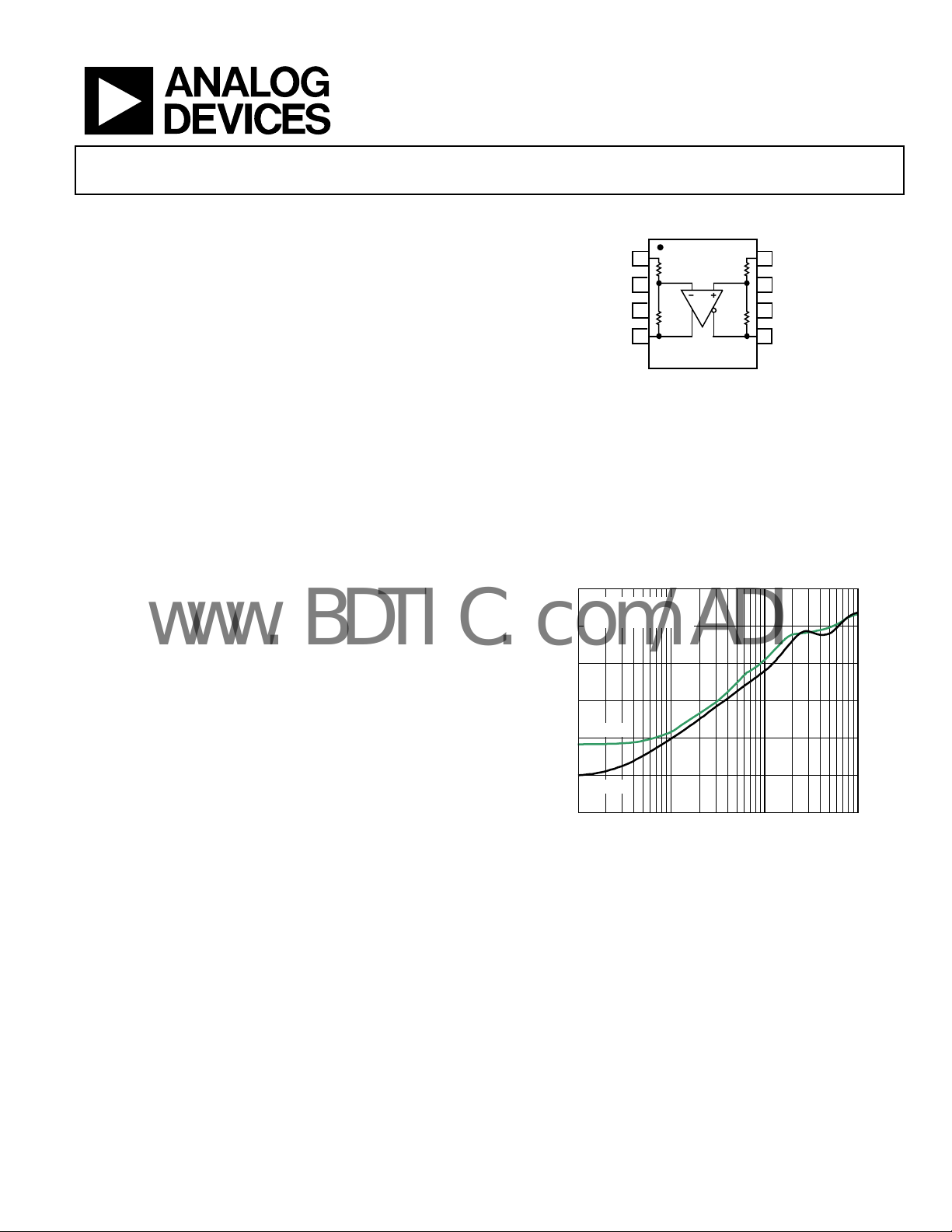
FUNCTIONAL BLOCK DIAGRAM
1
–D
IN
750Ω 750Ω
2
V
OCM
3
V+
1.5kΩ 1.5kΩ
45
+OUT
AD8131
NC = NO CONNECT
Figure 1.
20
= 2V p-p
ΔV
OUT, dm
/ΔV
ΔV
OUT, cm
–30
–40
–50
VS = +5V
–60
BALANCE ERROR (dB)
–70
V
= ±5V
S
–80
1 10 100 1000
Figure 2. Output Balance Error vs. Frequency
OUT, dm
FREQUENCY (MHz)
The AD8131’s differential output also helps balance the input
for differential ADCs, optimizing the distortion performance of
the ADCs. The common-mode level of the differential output is
adjustable by a voltage on the V
pin, easily level-shifting the
OCM
input signals for driving single-supply ADCs with dual supply
signals. Fast overload recovery preserves sampling accuracy.
The AD8131 is available in both SOIC and MSOP packages for
o
peration over −40°C to +125°C.
One Technology Way, P.O. Box 9106, Norwood, MA 02062-9106, U.S.A.
Tel: 781.329.4700 www.analog.com
Fax: 781.461.3113 ©2005 Analog Devices, Inc. All rights reserved.
+D
8
IN
7
NC
6
V–
–OUT
01072-001
01072-002

AD8131
www.BDTIC.com/ADI
TABLE OF CONTENTS
Specifications..................................................................................... 3
±D
to ±OUT Specifications...................................................... 3
IN
V
to ±OUT Specifications..................................................... 4
OCM
±D
to ±OUT Specifications...................................................... 5
IN
V
to ±OUT Specifications..................................................... 6
OCM
Absolute Maximum Ratings............................................................ 7
ESD Caution.................................................................................. 7
Pin Configuration and Function Descriptions............................. 8
Typical Performance Characteristics............................................. 9
Operational Description................................................................ 15
Theory of Operation ...................................................................... 16
Analyzing an Application Circuit.............................................16
Closed-Loop Gain...................................................................... 16
Estimating the Output Noise Voltage...................................... 16
Calculating the Input Impedance of an
Application Circuit..................................................................... 16
Input Common-Mode Voltage Range in
Single-Supply Applications .......................................................17
Setting the Output Common-Mode Voltage.......................... 17
Driving a Capacitive Load......................................................... 17
Applications..................................................................................... 18
Twisted-Pair Line Driver........................................................... 18
3 V Supply Differential A-to-D Driver.................................... 18
Unity-Gain, Single-Ended-to-Differential Driver ................. 19
Outline Dimensions .......................................................................20
Ordering Guide .......................................................................... 20
REVISION HISTORY
6/05—Rev. A to Rev. B
Updated Format..................................................................Universal
Changed Upper Operating Limit.....................................Universal
Changes to Ordering Guide.......................................................... 20
Rev. B | Page 2 of 20

AD8131
www.BDTIC.com/ADI
SPECIFICATIONS
±DIN TO ±OUT SPECIFICATIONS
25°C, VS = ±5 V, V
descriptions. All specifications refer to single-ended input and differential outputs, unless otherwise noted.
Table 1.
Parameter Conditions Min Typ Max Unit
DYNAMIC PERFORMANCE
−3 dB Large Signal Bandwidth V
−3 dB Small Signal Bandwidth V
Bandwidth for 0.1 dB Flatness V
Slew Rate V
Settling Time 0.1%, V
Overdrive Recovery Time VIN = 5 V to 0 V Step 5 ns
NOISE/HARMONIC PERFORMANCE
Second Harmonic V
V
V
V
Third Harmonic V
V
V
V
IMD 20 MHz, R
IP3 20 MHz, R
Voltage Noise (RTO) f = 20 MHz 25 nV/√Hz
Differential Gain Error NTSC, R
Differential Phase Error NTSC, R
INPUT CHARACTERISTICS
Input Resistance Single-ended input 1.125 kΩ
Differential input 1.5 kΩ
Input Capacitance 1 pF
Input Common-Mode Voltage −7.0 to +5.0 V
CMRR ΔV
OUTPUT CHARACTERISTICS
Offset Voltage (RTO) V
T
V
T
Output Voltage Swing Maximum ΔV
Linear Output Current 60 mA
Gain ΔV
Output Balance Error ΔV
= 0 V, G = 2, R
OCM
= 200 Ω, unless otherwise noted. Refer to Figure 5 and Figure 39 for test setup and label
L, dm
= 2 V p-p 400 MHz
OUT
= 0.2 V p-p 320 MHz
OUT
= 0.2 V p-p 85 MHz
OUT
= 2 V p-p, 10% to 90% 2000 V/μs
OUT
= 2 V p-p 14 ns
OUT
= 2 V p-p, 5 MHz, R
OUT
= 2 V p-p, 20 MHz, R
OUT
= 2 V p-p, 5 MHz, R
OUT
= 2 V p-p, 20 MHz, R
OUT
= 2 V p-p, 5 MHz, R
OUT
= 2 V p-p, 20 MHz, R
OUT
= 2 V p-p, 5 MHz, R
OUT
= 2 V p-p, 20 MHz, R
OUT
= 800 Ω −54 dBc
L, dm
= 800 Ω 30 dBm
L, dm
= 150 Ω 0.01 %
L, dm
= 150 Ω 0.06 degrees
L, dm
/ΔV
OUT, dm
= V
OS, dm
to T
MIN
= float ±4 mV
OCM
to T
MIN
OUT, dm
OUT, cm
; ΔV
IN, cm
; V
OUT, dm
DIN+
variation ±8 μV/°C
MAX
variation ±10 μV/°C
MAX
; single-ended output −3.6 to +3.6 V
OUT
/ΔV
; ΔV
IN, dm
/ΔV
OUT, dm
; ΔV
= 200 Ω −68 dBc
L, dm
= 200 Ω −63 dBc
L, dm
= 800 Ω −95 dBc
L, dm
= 800 Ω −79 dBc
L, dm
= 200 Ω −94 dBc
L, dm
= 200 Ω −70 dBc
L, dm
= 800 Ω −101 dBc
L, dm
= 800 Ω −77 dBc
L, dm
= ±0.5 V −70 dB
IN, cm
= V
= V
DIN−
= ±0.5 V 1.97 2 2.03 V/V
IN, dm
OUT, dm
= 0 V ±2 ±7 mV
OCM
= 1 V −70 dB
Rev. B | Page 3 of 20

AD8131
www.BDTIC.com/ADI
V
TO ±OUT SPECIFICATIONS
OCM
25°C, VS = ±5 V, V
descriptions. All specifications refer to single-ended input and differential outputs, unless otherwise noted.
Table 2.
Parameter Conditions Min Typ Max Unit
DYNAMIC PERFORMANCE
−3 dB Bandwidth ΔV
Slew Rate V
DC PERFORMANCE
Input Voltage Range ±3.6 V
Input Resistance 120 kΩ
Input Offset Voltage V
V
Input Bias Current 0.5 μA
VOCM CMRR ΔV
Gain ΔV
POWER SUPPLY
Operating Range ±1.4 ± 5.5 V
Quiescent Current V
T
Power Supply Rejection Ratio ΔV
OPERATING TEMPERATURE RANGE −40 +125 °C
= 0 V, G = 2, R
OCM
= 200 Ω, unless otherwise noted. Refer to Figure 5 and Figure 39 for test setup and label
L, dm
= 600 mV 210 MHz
OCM
= −1 V to +1 V 500 V/μs
OCM
= V
OS, cm
= float ±2.5 mV
OCM
OUT, dm
OUT, cm
= V
DIN+
to T
MIN
OUT, dm
; V
= V
= V
OUT, cm
DIN+
DIN−
/ΔV
; ΔV
OCM
/ΔV
OCM
= V
DIN−
variation 25 μA/°C
MAX
= ±0.5 V −60 dB
OCM
; ΔV
= ±1 V 0.988 1 1.012 V/V
OCM
= 0 V 10.5 11.5 12.5 mA
OCM
= 0 V ±1.5 ±7 mV
OCM
/ΔVS; ΔVS = ±1 V −70 −56 dB
Rev. B | Page 4 of 20
AD8131
www.BDTIC.com/ADI
±DIN TO ±OUT SPECIFICATIONS
25°C, VS = 5 V, V
descriptions. All specifications refer to single-ended input and differential outputs, unless otherwise noted.
Table 3.
Parameter Conditions Min Typ Max Unit
DYNAMIC PERFORMANCE
−3 dB Large Signal Bandwidth V
−3 dB Small Signal Bandwidth V
Bandwidth for 0.1 dB Flatness V
Slew Rate V
Settling Time 0.1%, V
Overdrive Recovery Time VIN = 5 V to 0 V Step
NOISE/HARMONIC PERFORMANCE
Second Harmonic V
Third Harmonic V
IMD 20 MHz, R
IP3 20 MHz, R
Voltage Noise (RTO) f = 20 MHz
Differential Gain Error NTSC, R
Differential Phase Error NTSC, R
INPUT CHARACTERISTICS
Input Resistance Single-ended input
Input Capacitance
Input Common-Mode Voltage
CMRR ΔV
OUTPUT CHARACTERISTICS
Offset Voltage (RTO) V
Output Voltage Swing Maximum ΔV
Linear Output Current
Gain ΔV
Output Balance Error ΔV
= 2.5 V, G = 2, R
OCM
= 200 Ω, unless otherwise noted. Refer to Figure 5 and Figure 39 for test setup and label
L, dm
= 2 V p-p
OUT
= 0.2 V p-p
OUT
= 0.2 V p-p
OUT
= 2 V p-p, 10% to 90%
OUT
= 2 V p-p
OUT
385
285
65
1600
18
5
MHz
MHz
MHz
V/μs
ns
ns
= 2 V p-p, 5 MHz, R
OUT
= 2 V p-p, 20 MHz, R
V
OUT
= 2 V p-p, 5 MHz, R
V
OUT
= 2 V p-p, 20 MHz, R
V
OUT
= 2 V p-p, 5 MHz, R
OUT
= 2 V p-p, 20 MHz, R
V
OUT
= 2 V p-p, 5 MHz, R
V
OUT
= 2 V p-p, 20 MHz, R
V
OUT
= 800 Ω
L, dm
= 800 Ω
L, dm
= 150 Ω
L, dm
= 150 Ω
L, dm
L, dm
L, dm
L, dm
L, dm
L, dm
L, dm
L, dm
L, dm
= 200 Ω
= 200 Ω
= 800 Ω
= 800 Ω
= 200 Ω
= 200 Ω
= 800 Ω
= 800 Ω
−67
−56
−94
−77
−74
−67
−95
−74
−51
29
25
0.02
0.08
dBc
dBc
dBc
dBc
dBc
dBc
dBc
dBc
dBc
dBm
nV/√Hz
%
degrees
Differential input
/ΔV
; ΔV
OUT, dm
IN, cm
IN, cm
= ±0.5 V
1.125
1.5
1
−1.0 to +4.0
−70
kΩ
kΩ
pF
V
dB
= V
OS, dm
to T
T
MIN
= float
V
OCM
to T
T
MIN
OUT, dm
OUT, cm
OUT, dm
variation
MAX
variation
MAX
/ΔV
IN, dm
/ΔV
OUT, dm
; V
= V
DIN+
; single-ended output
OUT
; ΔV
; ΔV
= V
DIN−
= ±0.5 V 1.96 2 2.04 V/V
IN, dm
= 1 V
OUT, dm
OCM
= 2.5 V
±3 ±7 mV
±8
±4
±10
1.0 to 3.7
45
−62
μV/°C
mV
μV/°C
V
mA
dB
Rev. B | Page 5 of 20

AD8131
www.BDTIC.com/ADI
V
TO ±OUT SPECIFICATIONS
OCM
25°C, VS = 5 V, V
descriptions. All specifications refer to single-ended input and differential outputs, unless otherwise noted.
Table 4.
Parameter Conditions Min Typ Max Unit
DYNAMIC PERFORMANCE
−3 dB Bandwidth ΔV
Slew Rate V
DC PERFORMANCE
Input Voltage Range
Input Resistance
Input Offset Voltage V
Input Bias Current
V
CMRR ΔV
OCM
Gain ΔV
POWER SUPPLY
Operating Range
Quiescent Current V
Power Supply Rejection Ratio ΔV
OPERATING TEMPERATURE RANGE
= 2.5 V, G = 2, R
OCM
= 200 Ω, unless otherwise noted. Refer to Figure 5 and Figure 39 for test setup and label
L, dm
= 600 mV
OCM
= 1.5 V to 3.5 V
OCM
200
450
MHz
V/μs
V
OS, cm
OCM
= V
= float
OUT, cm
; V
DIN+
= V
DIN−
= V
OCM
= 2.5 V
/ΔV
; ΔV
OUT, dm
OUT, cm
/ΔV
OCM
OCM
= 2.5 V ±0.5 V
OCM
; ΔV
= 2.5 V ±1 V 0.985 1 1.015 V/V
OCM
1.0 to 3.7
30
±5 ±12 mV
±10
0.5
−60
V
kΩ
mV
μA
dB
T
= V
DIN+
DIN−
to T
MIN
MAX
/ΔVS; ΔVS = ±0.5 V
OUT, dm
2.7
= V
= 2.5 V 9.25 10.25 11.25 mA
OCM
variation
20
−70 −56 dB
−40 +125 °C
11 V
μA/°C
Rev. B | Page 6 of 20

AD8131
www.BDTIC.com/ADI
ABSOLUTE MAXIMUM RATINGS
Table 5.
Parameter Rating
Supply Voltage ±5.5 V
V
Internal Power Dissipation 250 mW
Operating Temperature Range −40°C to +125°C
Storage Temperature Range −65°C to +150°C
Lead Temperature (Soldering 10 sec) 300°C
1
1
OCM
Thermal resistance measured on SEMI standard 4-layer board.
8-lead SOIC: θJA = 121°C/W.
8-lead MSOP: θJA = 142°C/W.
±V
S
Stresses above those listed under Absolute Maximum Ratings
may cause permanent damage to the device. This is a stress
rating only, functional operation of the device at these or any
other conditions above those indicated in the operational
section of this specification is not implied. Exposure to absolute
maximum rating conditions for extended periods may affect
device reliability.
2.0
TJ = 150°C
8-LEAD SOIC
1.5
1.0
0.5
MAXIMUM POWER DISSIPATION (W)
PACKAGE
8-LEAD
MSOP
PACKAGE
0
Figure 3. Plot of Maximum Power Dissipation vs. Temperature
–50
–20 10
AMBIENT TEMPERATURE (°C)
40 70
ESD CAUTION
ESD (electrostatic discharge) sensitive device. Electrostatic charges as high as 4000 V readily accumulate on
the human body and test equipment and can discharge without detection. Although this product features
proprietary ESD protection circuitry, permanent damage may occur on devices subjected to high energy
electrostatic discharges. Therefore, proper ESD precautions are recommended to avoid performance
degradation or loss of functionality.
100 130
01072-044
Rev. B | Page 7 of 20

AD8131
www.BDTIC.com/ADI
PIN CONFIGURATION AND FUNCTION DESCRIPTIONS
–D
1
IN
750Ω 750Ω
2
V
OCM
3
V+
1.5kΩ 1.5kΩ
45
+OUT
AD8131
NC = NO CONNECT
Figure 4. Pin Configuration
Table 6. Pin Function Descriptions
Pin No. Mnemonic Description
1 −D
2 V
IN
OCM
Negative Input.
Common-Mode Output Voltage. Voltage applied to this pin sets the common-mode output voltage with a ratio of
1:1. For example, 1 V dc on V
will set the dc bias level on +OUT and −OUT to 1 V.
OCM
3 V+ Positive Supply Voltage.
4 +OUT Positive Output. Note: the voltage at −DIN is inverted at +OUT.
5 −OUT Negative Output. Note: the voltage at +DIN is inverted at −OUT.
6 V− Negative Supply Voltage.
7 NC No Connect.
8 +D
IN
Positive Input.
8
+D
IN
7
NC
6
V–
–OUT
01072-003
Rev. B | Page 8 of 20

AD8131
www.BDTIC.com/ADI
TYPICAL PERFORMANCE CHARACTERISTICS
12
V
= 2V p-p
OUT
V
= ±5V
S
9
6
GAIN (dB)
3
MSOP
SOIC
49.9Ω
750Ω
750Ω
1500Ω
AD8131
R
L, dm
= 200Ω
24.9Ω
1500Ω
Figure 5. Basic Test Circuit
12
V
= 200mV p-p
OUT
V
= ±5V
S
9
6
GAIN (dB)
3
0
–3
1 10 100 1000
FREQUENCY (MHz)
MSOP
SOIC
Figure 6. Small S ignal Freq uency Respons e
12
V
= 200mV p-p
OUT
9
01072-004
01072-005
0
–3
1 10 100 1000
FREQUENCY (MHz)
Figure 8. Large S ignal Frequenc y Respons e
12
V
= 2V p-p
OUT
9
V
6
= +5V
V
GAIN (dB)
3
0
–3
1 10 100 1000
FREQUENCY (MHz)
S
S
Figure 9. Large S ignal Frequenc y Respons e
01072-007
= ±5V
01072-008
= ±5V
V
6
GAIN (dB)
3
0
–3
1 10 100 1000
FREQUENCY (MHz)
V
= +5V
S
Figure 7. Small S ignal Freq uency Respons e
S
LPF
49.9Ω
24.9Ω
01072-006
750Ω
750Ω
Figure 10. Harmonic Distortion Test Circuit (R
Rev. B | Page 9 of 20
1500Ω
AD8131
1500Ω
2:1 TRANSFORMER
300Ω
300Ω
Z
HPF
= 50Ω
IN
01072-009
= 800 Ω)
L, dm

AD8131
–
–
www.BDTIC.com/ADI
50
–60
–70
–80
–90
DISTORTION (dBc)
R
L, dm
V
OUT, dm
HD3 (V
= 800Ω
= 1V p-p
= 3V)
S
HD2 (V
HD2 (V
= 5V)
S
= 3V)
S
HD3 (V
= 5V)
S
50
VS = 5V
R
L, dm
–60
–70
–80
–90
DISTORTION (dBc)
= 800Ω
HD3 (F = 20MHz)
HD2 (F = 20MHz)
HD3 (F = 5MHz)
–100
–110
0102030
Figure 11. Harmonic Distortion vs. Frequency
–40
R
= 800Ω
L, dm
V
= 2V p-p
OUT, dm
–50
= +5V)
HD3 (V
–60
–70
–80
DISTORTION (dBc)
–90
–100
–110
0102030
S
HD2 (V
Figure 12. Harmonic Distortion vs. Frequency
–55
VS = ±5V
= 800Ω
R
L, dm
–65
–75
–85
FREQUENCY (M Hz )
40 50 60 70
= ±5V)
HD3 (V
S
HD2 (V
= +5V)
S
FREQUENCY (MHz)
40 50 60 70
HD3 (F = 20MHz)
HD2 (F = 20MHz)
= ±5V)
S
01072-010
01072-011
–100
–110
1.0 1.5 2.00.50
DIFFERENTIAL OUTPUT VOLTAGE (V p-p)
HD2 (F = 5MHz)
2.5 3.0 3.5 4.0
Figure 14. Harmonic Distortion vs. Differential Output Voltage
–50
DISTORTION (dBc)
–100
–110
–60
–70
–80
–90
VS = 3V
R
= 800Ω
L, dm
HD3 (F = 20MHz)
0.75 1.00.500.25
DIFFERENTIAL OUTPUT VOLTAGE (V p-p)
HD3 (F = 5MHz)
HD2 (F = 20MHz)
HD2 (F = 5MHz)
1.25 1.5 1.75
Figure 15. Harmonic Distortion vs. Differential Output Voltage
–50
VS = ±5V
= 2V p-p
V
OUT, dm
–60
HD2 (F = 20MHz)
–70
–80
HD3 (F = 20MHz)
01072-013
01072-014
–95
DISTORTION (dBc)
–105
–115
012
HD2 (F = 5MHz)
DIFFERENTIAL OUTPUT VOLTAGE (V p-p)
HD3 (F = 5MHz)
3456
Figure 13. Harmonic Distortion vs. Differential Output Voltage
01072-012
DISTORTION (dBc)
–100
–110
HD2 (F = 5MHz)
HD3 (F = 5MHz)
400 500 600300200
Figure 16. Harmonic Distortion vs. R
–90
Rev. B | Page 10 of 20
R
700 800 900 1000
(Ω)
LOAD
01072-015
LOAD

AD8131
–
www.BDTIC.com/ADI
DISTORTION (dBc)
–100
–60
–70
–80
–90
50
VS = 5V
V
= 2V p-p
OUT, dm
HD2 (F = 20MHz)
HD2 (F = 5MHz)
HD3 (F = 5MHz)
HD3 (F = 20MHz)
45
40
35
30
INTERCEPT (dBm)
25
20
R
L, dm
VS = +5V
= 800Ω
VS = ±5V
–110
400 500 600300200
R
Figure 17. Harmonic Distortion vs. R
–50
VS = 3V
= 1V p-p
V
OUT, dm
DISTORTION (dBc)
–100
–110
–60
–70
–80
–90
HD2 (F = 20MHz)
HD2 (F = 5MHz)
400 500 600300200
R
Figure 18. Harmonic Distortion vs. R
10
f
= 500MHz
C
0
V
= ±5V
S
–10
R
= 800Ω
L, dm
–20
–30
–40
(dBm)
–50
OUT
–60
P
–70
–80
–90
–100
–110
49.5 50.0 50.5
FREQUENCY (MHz)
700 800 900 1000
(Ω)
LOAD
HD3 (F = 20MHz)
HD3 (F = 5MHz)
700 800 900 1000
(Ω)
LOAD
LOAD
LOAD
Figure 19. Intermodulation Distortion
01072-016
01072-017
01072-018
15
20 30 40100
FREQUENCY (MHz)
Figure 20. Third Order Intercept vs. Frequency
V
OUT, dm
V
OUT+
V
OUT–
V
+DIN
1V
Figure 21. Large Signal Transient Response
VS = +5V
VS = ±5V
40mV
Figure 22. Small Signal Transient Response
50 60 70 80
VS = ±5V
5ns
5ns
01072-020
01072-021
01072-019
Rev. B | Page 11 of 20

AD8131
www.BDTIC.com/ADI
V
= 2V p-p
VS = +5V
VS = ±5V
400mV
OUT
5ns
Figure 23. Large Signal Transient Response
V
= 1.5V p-p
OUT
VS = 3V
01072-022
1500Ω
750Ω
49.9Ω
24.9Ω
750Ω
AD8131
1500Ω
Figure 26. Capacitor Load Drive Test Circuit
CL = 0pF
CL = 5pF
CL = 20pF
24.9Ω
24.9Ω
C
L
VS = ±5V
150Ω
01072-025
Figure 24. Large Signal Transient Response
2mV/DIV
V
OUT, dm
1V/DIV
V
+DIN
Figure 25. 0.1% Settling Time
4ns
5ns300mV
VS = ±5V
01072-023
01072-024
400mV
1.25ns
01072-026
Figure 27. Large Signal Transient Response for Various Capacitor Loads
0
ΔV
OUT, dm
–10
ΔV
S
–20
–30
–40
PSRR (dB)
–50
–60
–70
–80
+PSRR
(V
= ±5V, +5V)
S
–PSRR
(V
= ±5V)
S
1 100 1000
10
FREQUENCY (MHz)
01072-027
Figure 28. PSRR v s. Frequency
Rev. B | Page 12 of 20

AD8131
www.BDTIC.com/ADI
1500Ω
24.9Ω
750Ω
750Ω
AD8131
1500Ω
100Ω
V
OUT, dm
100Ω
Figure 29. CMRR Test Circuit
–20
VS = ±5V
V
= 1V p-p
IN, cm
–30
–40
–50
ΔV
/ΔV
OUT, dm
CMRR (dB)
–60
–70
–80
1 10 100 1000
ΔV
OUT, cm
IN, cm
/ΔV
IN, cm
FREQUENCY (MHz)
Figure 30. CMRR vs. Frequen cy
100
SINGLE-ENDED OUTPUT
10
V
OUT, cm
01072-028
01072-029
1500Ω
49.9Ω
24.9Ω
750Ω
750Ω
AD8131
1500Ω
100Ω
100Ω
Figure 32. Output Balance Error Test Circuit
–20
ΔV
= 2V p-p
OUT, dm
ΔV
/ΔV
OUT, cm
–30
–40
–50
VS = +5V
–60
BALANCE ERROR (dB)
–70
V
= ±5V
S
–80
1 10 100 1000
OUT, dm
FREQUENCY (MHz)
Figure 33. Output Balance Error vs. Frequency
15
13
11
VS = ±5V
VS = +5V
01072-031
01072-032
IMPEDANCE (Ω)
1
0.1
1 10 100
Figure 31. Single-Ended Z
VS = +5V
VS = ±5V
FREQUENCY (MHz)
vs. Frequency
OUT
01072-030
9
SUPPLY CURRENT (mA)
7
5
–50 –20 10 40
Figure 34. Quiescent Current vs. Temperature
Rev. B | Page 13 of 20
TEMPERATURE (°C)
70 100 130
01072-034

AD8131
www.BDTIC.com/ADI
110
90
Hz)
70
√
50
NOISE (nV/
30
VS = ±5V
–20
–30
–40
–50
–60
CMRR (dB)
–70
–80
ΔV
OUT, cm
ΔV
OCM
ΔV
OCM
= 600mV p-p
ΔV
OCM
VS = ±5V
= 2V p-p
10
0.1k 1k 10k 100k
FREQUENCY (Hz)
1M 10M 100M
Figure 35. Voltage Noise vs. Frequency
6
ΔV
OUT, cm
ΔV
OCM
3
0
GAIN (dB)
–3
ΔV
–6
–9
1 10 100 1000
Figure 36. V
OCM
FREQUENCY (MHz)
OCM
ΔV
OCM
= 2V p-p
Gain Response
VS = ±5V
= 600mV p-p
01072-035
01072-036
–90
1 10 100 1000
Figure 37. V
FREQUENCY (MHz)
CMRR vs. Frequency
OCM
VS= 5V
= –1V TO +1V
V
OCM
400mV
V
OUT, cm
5ns
Figure 38. V
Transient Response
OCM
01072-038
01072-037
Rev. B | Page 14 of 20

AD8131
(
)
(
)
+
=
www.BDTIC.com/ADI
OPERATIONAL DESCRIPTION
R
F
R
G
+D
IN
V
OCM
–D
IN
+IN
–IN
R
G
Figure 39. Circuit Definitions
AD8131
R
F
–OUT
+OUT
R
L, dm
–OUT
V
OUT, dm
+OUT
01072-039
Differential voltage refers to the difference between two node
voltages. For example, the output differential voltage (or
equivalently output differential-mode voltage) shown in
Figure 39 is defined as
VVV
,
dmOUT
−=
OUTOUT
−+
Common-mode voltage refers to the average of two node
oltages. The output common-mode voltage is defined as
v
, OUTOUTcmOUT
VVV
2
−+
Balance is a measure of how well differential signals are
matched in amplitude and exactly 180 degrees apart in phase.
Balance is most easily determined by placing a well-matched
resistor divider between the differential voltage nodes and
comparing the magnitude of the signal at the divider’s midpoint
with the magnitude of the differential signal. By this definition,
output balance is the magnitude of the output common-mode
voltage divided by the magnitude of the output differentialmode voltage.
V
+OUT
and V
refer to the voltages at the +OUT and −OUT
–OUT
terminals with respect to a common reference.
V
cmOUT
ErrorBalanceOutput
=
,
V
dmOUT
,
Rev. B | Page 15 of 20

AD8131
Ω=×
=
www.BDTIC.com/ADI
THEORY OF OPERATION
The AD8131 differs from conventional op amps in that it has
two outputs whose voltages move in opposite directions. Like
an op amp, it relies on high open-loop gain and negative
feedback to force these outputs to the desired voltages. The
AD8131 behaves much like a standard voltage feedback op amp
and makes it easy to perform single-ended-to-differential
conversion, common-mode level-shifting, and amplification of
differential signals.
Previous discrete and integrated differential driver designs used
tw
o independent amplifiers and two independent feedback
loops, one to control each of the outputs. When these circuits
are driven from a single-ended source, the resulting outputs are
typically not well balanced. Achieving a balanced output
typically required exceptional matching of the amplifiers and
feedback networks.
DC common-mode level shifting has also been difficult with
revious differential drivers. Level shifting required the use of a
p
third amplifier and feedback loop to control the output
common-mode level. Sometimes the third amplifier has also
been used to attempt to correct an inherently unbalanced
circuit. Excellent performance over a wide frequency range has
proven difficult with this approach.
The AD8131 uses two feedback loops to separately control the
ferential and common-mode output voltages. The differential
dif
feedback, set by internal resistors, controls only the differential
output voltage. The common-mode feedback controls only the
common-mode output voltage. This architecture makes it easy
to arbitrarily set the common-mode output level. It is forced, by
internal common-mode feedback, to be equal to the voltage
applied to the V
output voltage.
The AD8131 architecture results in outputs that are very highly
alanced over a wide frequency range without requiring
b
external components or adjustments. The common-mode
feedback loop forces the signal component of the output
common-mode voltage to be zeroed. The result is nearly
perfectly balanced differential outputs, of identical amplitude
and exactly 180 degrees apart in phase.
ANALYZING AN APPLICATION CIRCUIT
The AD8131 uses high open-loop gain and negative feedback to
force its differential and common-mode output voltages in such
a way as to minimize the differential and common-mode error
voltages. The differential error voltage is defined as the voltage
between the differential inputs labeled +IN and −IN in
Figure 39. For most purposes, this voltage can be assumed to be
zer
o. Similarly, the difference between the actual output
common-mode voltage and the voltage applied to V
input, without affecting the differential
OCM
can also
OCM
be assumed to be zero. Starting from these two assumptions,
any application circuit can be analyzed.
CLOSED-LOOP GAIN
The differential mode gain of the circuit in Figure 39 can be
described by the following equation:
where
V
V
R
= 1.5 kΩ and RG = 750 Ω nominally.
F
R
dmOUT,
F
2==
R
dmIN,
G
ESTIMATING THE OUTPUT NOISE VOLTAGE
Similar to the case of a conventional op amp, the differential
output errors (noise and offset voltages) can be estimated by
multiplying the input referred terms, at +IN and −IN, by the
circuit noise gain. The noise gain is defined as
G
N
⎜
⎝
31 =
⎟
R
G
⎠
⎛
⎞
R
F
⎜
⎟
+=
The total output referred noise for the AD8131, including the
ntributions of R
co
, RG, and op amp, is nominally 25 nV/√Hz
F
at 20 MHz.
CALCULATING THE INPUT IMPEDANCE OF AN APPLICATION CIRCUIT
The effective input impedance of a circuit such as that in
Figure 39, at +D
amplifier is being driven by a single-ended or differential signal
source. For balanced differential input signals, the input
impedance (R
,GdmIN
In the case of a single-ended input signal (for example if −D
grounded and the input signal is applied to +D
impedance becomes
R
dmIN
,
The input impedance is effectively higher than it would be for a
nventional op amp connected as an inverter because a
co
fraction of the differential output voltage appears at the inputs
as a common-mode signal, partially bootstrapping the voltage
across the input resistor R
and −DIN, will depend on whether the
IN
) between the inputs (+DIN and −DIN) is
IN, dm
RR
⎛
⎜
⎜
= k 125.1
⎜
−
1
⎜
⎜
⎝
k5.12
⎞
R
G
R
()
2
G
⎟
⎟
⎟
F
⎟
⎟
+×
RR
F
⎠
.
G
Ω=
), the input
IN
is
IN
Rev. B | Page 16 of 20

AD8131
www.BDTIC.com/ADI
INPUT COMMON-MODE VOLTAGE RANGE IN SINGLE-SUPPLY APPLICATIONS
The AD8131 is optimized for level-shifting ground referenced
input signals. For a single-ended input this would imply, for
example, that the voltage at −D
volts when the amplifier’s negative power supply voltage (at V−)
was also set to zero volts.
in Figure 39 would be zero
IN
SETTING THE OUTPUT COMMON-MODE VOLTAGE
The AD8131’s V
approximately equal to the midsupply point (average value of
the voltages on V+ and V−). Relying on this internal bias results
in an output common-mode voltage that is within about 25 mV
of the expected value.
pin is internally biased at a voltage
OCM
In cases where more accurate control of the output commonm
ode level is required, it is recommended that an external
source, or resistor divider (made up of 10 kΩ resistors), be used.
DRIVING A CAPACITIVE LOAD
A purely capacitive load can react with the pin and bondwire
inductance of the AD8131 resulting in high frequency ringing
in the pulse response. One way to minimize this effect is to
place a small resistor in series with the amplifier’s outputs as
shown in
Figure 26.
Rev. B | Page 17 of 20

AD8131
www.BDTIC.com/ADI
APPLICATIONS
TWISTED-PAIR LINE DRIVER
The AD8131 has on-chip resistors that provide for a gain of 2
without any external parts. Several on-chip resistors are
trimmed to ensure that the gain is accurate, the common-mode
rejection is good, and the output is well balanced. This makes
the AD8131 very suitable as a single-ended-to-differential
twisted-pair line driver.
3 V SUPPLY DIFFERENTIAL A-TO-D DRIVER
Many newer ADCs can run from a single 3 V supply, which can
save significant system power. In order to increase the dynamic
range at the analog input, they have differential inputs, which
double the dynamic range with respect to a single-ended input.
An added benefit of using a differential input is that the
distortion can be improved.
Figure 40 shows a circuit of an AD8131 driving a twisted-pair
, like a Category 3 or Category 5 (Cat3 or Cat5), that is
line
already installed in many buildings for telephony and data
communications. The characteristic impedance of such a
transmission line is usually about 100 Ω. The outstanding
balance of the AD8131 output will minimize the commonmode signal and therefore the amount of EMI generated by
driving the twisted pair.
The two resistors in series with each output terminate the line at
he transmit end. Since the impedances of the outputs of the
t
AD8131 are very low, they can be thought of as a short-circuit,
and the two terminating resistors form a 100 Ω termination at
the transmit end of the transmission line. The receive end is
directly terminated by a 100 Ω resistor across the line.
This back-termination of the transmission line divides the
o
utput signal by two. The fixed gain of 2 of the AD8131 will
create a net unity gain for the system from end to end.
In this case, the input signal is provided by a signal generator
wi
th an output impedance of 50 Ω. This is terminated with a
49.9 Ω resistor near +D
of the AD8131. The effective parallel
IN
resistance of the source and termination is 25 Ω.The 24.9 Ω
resistor from −D
to ground matches the +DIN source
IN
impedance and minimizes any dc and gain errors.
is driven by a low-impedance source over a short
If +D
IN
distance, such as the output of an op amp, then no termination
resistor is required at +D
. In this case, the −DIN can be directly
IN
tied to ground.
+5V
+
10
μ
0.1
μ
49.9
3
8
5
24.9Ω
2
AD8131
1
–5V
4
6
49.9
0.1
49.9Ω
Figure 40. Single-Ended-to-Differential 100 Ω Line Driver
F
F
Ω
100Ω
RECEIVER
Ω
10μF
μ
F
+
01072-040
The low distortion and ability to run from a single 3 V supply make
th
e AD8131 suited as an A-to-D driver for some 10-bit, singlesupply applications.
AD8131
driving an AD9203, a 10-bit, 40 MSPS ADC.
Figure 41 shows a schematic for a circuit for an
The common mode of the AD8131 output is set at midsupply
y the voltage divider connected to V
b
, and ac-bypassed with
OCM
a 0.1 μF capacitor. This provides for maximum dynamic range
between the supplies at the output of the AD8131. The 110 Ω
resistors at the AD8131 output, along with the shunt capacitors
form a one pole, low-pass filter for lowering noise and
antialiasing.
3V
+
10
F
F
0.1
110Ω
LPF
49.9Ω
10kΩ
10kΩ
+3V
0.1
24.9Ω
8
2
F
1
3
AD8131
V
OCM
6
110Ω
20pF
25
20pF
Figure 41. Test Circuit for AD8131 Driving an AD9203, 10-Bit, 40 MSPS ADC
3V
F
28
2
DRVDD
AVDD
26
AINN
AD9203
AINP
DRVSS
AVSS
27
0.1
DIGITAL
OUTPUTS
1
Figure 42 shows an FFT plot that was taken from the combined
devices at an analog input frequency of 2.5 MHz and a 40 MSPS
sampling rate. The performance of the AD8131 compares very
favorably with a center-tapped transformer drive, which has
typically been the best way to drive this ADC. The AD8131 has
the advantage of maintaining dc performance, which a
transformer solution cannot provide.
01072-041
Rev. B | Page 18 of 20

AD8131
www.BDTIC.com/ADI
10
0
–10
–20
–30
–40
(dBm)
–50
OUT
–60
P
–70
–80
–90
–100
–110
–120
2.0 2.1 2.2 2.3 2.4 2.5 2.6 2.7 2.8 2.9 3.0
FREQUENCY (MHz)
01072-042
Figure 42. FFT Plot for AD8131/AD9203
UNITY-GAIN, SINGLE-ENDED-TO-DIFFERENTIAL DRIVER
If it is not necessary to offset the output common-mode voltage
(via the V
gain single-ended-to-differential amplifier that does not require
any external components.
is circuit.
th
pin), then the AD8131 can make a simple unity-
OCM
Figure 43 shows the schematic for
49.9Ω
Figure 43. Unity Gain, Single-Ended-to-Differential Amplifier
As shown above, when −DIN is left floating, there is 100%
feedback of +OUT to −IN via the internal feedback resistor.
This contrasts with the typical gain of 2 operation where −D
grounded and one third of the +OUT is fed back to −IN. The
result is a closed-loop differential gain of 1.
Upon careful observation, it can be seen that only +D
are referenced to ground. The ground voltage at V
reference for this circuit. In this unity gain configuration, if a dc
voltage is applied to V
differential dc voltage will be created at the output, along with the
common-mode voltage change. Thus, this configuration cannot
be used when it is desired to offset the common-mode voltage of
the output with respect to the input at +D
+5V
+
10 F
0.1
F
3
8
5
2
AD8131
1
4
6
0.1
–5V
10 F
F
+
to shift the common-mode voltage, a
OCM
.
IN
OCM
INPUT
OUT
–
+OUT
and V
IN
is the
01072-043
is
IN
OCM
Rev. B | Page 19 of 20

AD8131
www.BDTIC.com/ADI
OUTLINE DIMENSIONS
5.00 (0.1968)
4.80 (0.1890)
4.00 (0.1574)
3.80 (0.1497)
0.25 (0.0098)
0.10 (0.0040)
COPLANARITY
0.10
CONTROLLING DIMENSIONS ARE IN MILLIMETERS; INCH DIMENSIONS
(IN PARENTHESES) ARE ROUNDED-OFF MILLIMETER EQUIVALENTS FOR
REFERENCE ONLY AND ARE NOT APPROPRIATE FOR USE IN DESIGN
85
1.27 (0.0500)
SEATING
PLANE
COMPLIANT TO JEDEC STANDARDS MS-012-AA
Figure 44. 8-Lead Standard Small Outline Package [SOIC_N]
Dimensions shown in millimeters and (inches)
BSC
6.20 (0.2440)
5.80 (0.2284)
41
1.75 (0.0688)
1.35 (0.0532)
0.51 (0.0201)
0.31 (0.0122)
row Body
Nar
(R-8)
0.25 (0.0098)
0.17 (0.0067)
0.50 (0.0196)
0.25 (0.0099)
8°
1.27 (0.0500)
0°
0.40 (0.0157)
× 45°
3.00
BSC
8
5
4
SEATING
PLANE
4.90
BSC
1.10 MAX
0.23
0.08
8°
0°
0.80
0.60
0.40
3.00
BSC
1
PIN 1
0.65 BSC
0.15
0.00
0.38
0.22
COPLANARITY
0.10
COMPLIANT TO JEDEC STANDARDS MO-187-AA
Figure 45. 8-Lead Mini Small Outline Package [MSOP]
(RM-8)
mensions shown in millimeters
Di
ORDERING GUIDE
Model Temperature Range Package Description Package Option Branding
AD8131AR −40°C to +125°C 8-Lead Standard Small Outline Package [SOIC_N] R-8
AD8131AR-REEL −40°C to +125°C 8-Lead SOIC, 13” Tape and Reel R-8
AD8131AR-REEL7 −40°C to +125°C 8-Lead SOIC, 7”
AD8131ARZ
AD8131ARZ-REEL
AD8131ARZ-REEL7
1
1
−40°C to +125°C 8-Lead Standard Small Outline Package [SOIC_N] R-8
−40°C to +125°C 8-Lead SOIC, 13” Tape and Reel R-8
1
−40°C to +125°C 8-Lead SOIC, 7” Tape and Reel R-8
AD8131ARM −40°C to +125°C 8-Lead Mini Sm
AD8131ARM-REEL −40°C to +125°C 8-Lead MSOP, 1
AD8131ARM-REEL7 −40°C to +125°C 8-Lead MSOP, 7
AD8131ARMZ
AD8131ARMZ-REEL
AD8131ARMZ-REEL7
1
Z = Pb-free part, # denotes Pb-free part; may be top or bottom marked.
1
−40°C to +125°C 8-Lead Mini Small Outline Package [MSOP] RM-8 HJA#
1
−40°C to +125°C 8-Lead MSOP, 13” Tape and Reel RM-8 HJA#
1
−40°C to +125°C 8-Lead MSOP, 7” Tape and Reel RM-8 HJA#
Tape and Reel R-8
all Outline Package [MSOP] RM-8 HJA
3” Tape and Reel RM-8 HJA
” Tape and Reel RM-8 HJA
©2005 Analog Devices, Inc. All rights reserved. Trademarks and
registered trademarks are the property of their respective owners.
C01072–0–6/05(B)
Rev. B | Page 20 of 20
 Loading...