Analog Devices AD8079 Datasheet

a
AD8079
FEATURES
Factory Set Gain
AD8079A: Gain = +2.0 (Also +1.0 & –1.0)
AD8079B: Gain = +2.2 (Also +1 & –1.2)
Gain of 2.2 Compensates for System Gain Loss
Minimizes External Components
Tight Control of Gain and Gain Matching (0.1%)
Optimum Dual Pinout
Simplifies PCB Layout
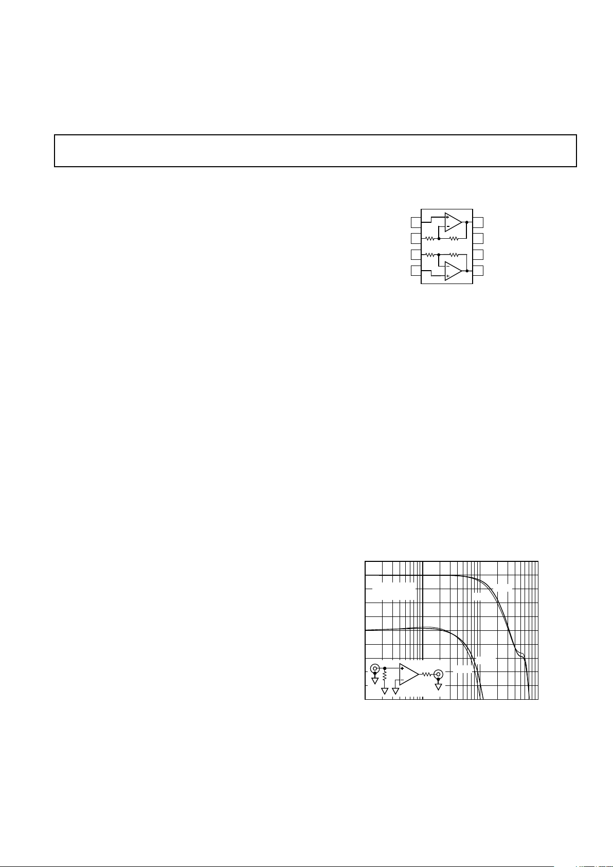
Low Crosstalk of –70 dB @ 5 MHz
Excellent Video Specifications (R
L
= 150 V)
Gain Flatness 0.1 dB to 50 MHz
0.01% Differential Gain Error
0.028 Differential Phase Error
Low Power of 50 mW/Amplifier (5 mA)
High Speed and Fast Settling
260 MHz, –3 dB Bandwidth
750 V/ms Slew Rate (2 V Step), 800 V/ms (4 V Step)
40 ns Settling Time to 0.1% (2 V Step)
Low Distortion of –65 dBc THD, f
C
= 5 MHz
High Output Drive of Over 70 mA
Drives Up to 8 Back-Terminated 75 V Loads (4 Loads/
Side) While Maintaining Good Differential Gain/
Phase Performance (0.01%/0.178)
High ESD Tolerance (5 kV)
Available in Small 8-Pin SOIC
APPLICATIONS
Differential A-to-D Driver
Video Line Driver
Differential Line Driver
Professional Cameras
Video Switchers
Special Effects
RF Receivers
FUNCTIONAL BLOCK DIAGRAM
8-Pin Plastic SOIC
1
2
3
4
5
6
7
8
AD8079
+IN1
GND
GND
+IN2
OUT1
+V
S
–V
S
OUT2
Dual 260 MHz
Gain = +2.0 & +2.2 Buffer
REV. A
Information furnished by Analog Devices is believed to be accurate and
reliable. However, no responsibility is assumed by Analog Devices for its
use, nor for any infringements of patents or other rights of third parties
which may result from its use. No license is granted by implication or
otherwise under any patent or patent rights of Analog Devices.
PRODUCT DESCRIPTION
The AD8079 is a dual, low power, high speed buffer designed
to operate on ± 5 V supplies. The AD8079’s pinout offers excellent input and output isolation compared to the traditional dual
amplifier pin configuration. With two ac ground pins separating
both the inputs and outputs, the AD8079 achieves very low
crosstalk of less than –70 dB at 5 MHz.
Additionally, the AD8079 contains gain setting resistors factory
set at G = +2.0 (A grade) or Gain = +2.2 (B grade) allowing
circuit configurations with minimal external components. The
B grade gain of +2.2 compensates for gain loss through a system
by providing a single-point trim. Using active laser trimming of
these resistors, the AD8079 guarantees tight control of gain and
channel-channel gain matching. With its performance and configuration, the AD8079 is well suited for driving differential
cables and transformers. Its low distortion and fast settling are
ideal for buffering high speed dual or differential A-to-D converters.
The AD8079 features a unique transimpedance linearization
circuitry. This allows it to drive video loads with excellent differential gain and phase performance of 0.01% and 0.02° on only
50 mW of power per amplifier. It features gain flatness of 0.1 dB
to 50 MHz. This makes the AD8079 ideal for professional video
electronics such as cameras and video switchers.
The AD8079 offers low power of 5 mA/amplifier (V
S
= ±5 V)
and can run on a single +12 V power supply while delivering
over 70 mA of load current. All of this is offered in a small 8-pin
SOIC package. These features make this amplifier ideal for portable and battery powered applications where size and power are
critical.
The outstanding bandwidth of 260 MHz along with 800 V/µs of
slew rate make the AD8079 useful in many general purpose high
speed applications where dual power supplies of ± 3 V to ±6 V
are required.
The AD8079 is available in the industrial temperature range of
–40°C to +85°C.
FREQUENCY – Hz
1M
NORMALIZED FLATNESS – dB
1G10M 100M
–0.5
0.1
0
–0.1
–0.2
–0.3
–0.4
1
0
–9
–1
–2
–3
–4
–5
–6
–7
–8
NORMALIZED FREQUENCY RESPONSE – dB
SIDE 2
SIDE 1
SIDE 2
SIDE 1
RL = 100Ω
VIN = 50mV rms
50Ω
50Ω
Figure 1. Frequency Response and Flatness
One Technology Way, P.O. Box 9106, Norwood, MA 02062-9106, U.S.A.
Tel: 617/329-4700 World Wide Web Site: http://www.analog.com
Fax: 617/326-8703 © Analog Devices, Inc., 1996

AD8079–SPECIFICATIONS
AD8079A/AD8079B
Parameter Conditions Min Typ Max Units
DYNAMIC PERFORMANCE
–3 dB Small Signal Bandwidth V
IN
= 50 mV rms 260 MHz
Bandwidth for 0.1 dB Flatness V
IN
= 50 mV rms 50 MHz
Large Signal Bandwidth V
IN
= 1 V rms 100 MHz
Slew Rate V
O
= 2 V Step 750 V/µs
V
O
= 4 V Step 800 V/µs
Settling Time to 0.1% V
O
= 2 V Step 40 ns
Rise & Fall Time VO = 2 V Step 2.5 ns
NOISE/HARMONIC PERFORMANCE
Total Harmonic Distortion f
C
= 5 MHz, VO = 2 V p-p –65 dBc
Crosstalk, Output to Output f = 5 MHz –70 dB
Input Voltage Noise f = 10 kHz 2.0 nV/√
Hz
Input Current Noise f = 10 kHz, +In 2.0 pA/√
Hz
Differential Gain Error NTSC, R
L
= 150 Ω 0.01 %
NTSC, R
L
= 75 Ω 0.01 %
Differential Phase Error NTSC, R
L
= 150 Ω 0.02 Degree
RL = 75 Ω 0.07 Degree
DC PERFORMANCE
Offset Voltage, RTO 10 15 mV
T
MIN–TMAX
10 20 mV
Offset Drift, RTO 20 µV/°C
+Input Bias Current 3.0 6.0 ±µA
T
MIN–TMAX
10 ±µA
Gain No Load 1.998/2.198 2.0/2.2 2.002/2.202 V/V
R
L
= 150 Ω 1.995/2.195 2.0/2.2 2.005/2.205 V/V
Gain Matching Channel-to-Channel, No Load 0.1 %
Channel-to-Channel, RL = 150 Ω 0.5 %
INPUT CHARACTERISTICS
+Input Resistance +Input 10 MΩ
+Input Capacitance +Input 1.5 pF
OUTPUT CHARACTERISTICS
Output Voltage Swing R
L
= 150 Ω 2.7 3.1 ±V
R
L
= 75 Ω 2.8 ±V
Output Current
1
70 mA
Short Circuit Current
1
85 110 mA
POWER SUPPLY
Operating Range ±3.0 ± 6.0 V
Quiescent Current/Both Amplifiers T
MIN–TMAX
10.0 11.5 mA
Power Supply Rejection Ratio, RTO +V
S
= +4 V to +6 V, –VS = –5 V 49 69 dB
–V
S
= – 4 V to – 6 V, +VS = +5 V 40 50 dB
+Input Current T
MIN–TMAX
0.1 0.5 µA/V
NOTES
1
Output current is limited by the maximum power dissipation in the package. See the power derating curves.
Specifications subject to change without notice.
–2–
REV. A
(@ TA = +258C, VS = 65 V, RL = 100 V, unless otherwise noted)

9
REV. A
AD8079
–3–
ABSOLUTE MAXIMUM RATINGS
1
Supply Voltage . . . . . . . . . . . . . . . . . . . . . . . . . . . . . . . . 12.6 V
Internal Power Dissipation
2
Small Outline Package (R) . . . . . . . . . . . . . . . . . . 0.9 Watts
Input Voltage . . . . . . . . . . . . . . . . . . . . . . . . . . . . . . . . . . . ±V
S
Output Short Circuit Duration
. . . . . . . . . . . . . . . . . . . . Observe Power Derating Curves
Storage Temperature Range . . . . . . . . . . . . .–65°C to +125°C
Operating Temperature Range (A Grade) . . . –40°C to +85°C
Lead Temperature Range (Soldering 10 sec) . . . . . . . . +300°C
NOTES
1
Stresses above those listed under “Absolute Maximum Ratings” may cause
permanent damage to the device. This is a stress rating only and functional
operation of the device at these or any other conditions above those indicated in the
operational section of this specification is not implied. Exposure to absolute
maximum rating conditions for extended periods may affect device reliability.
2
Specification is for device in free air:
8-Pin SOIC Package: θJA = 160°C/Watt
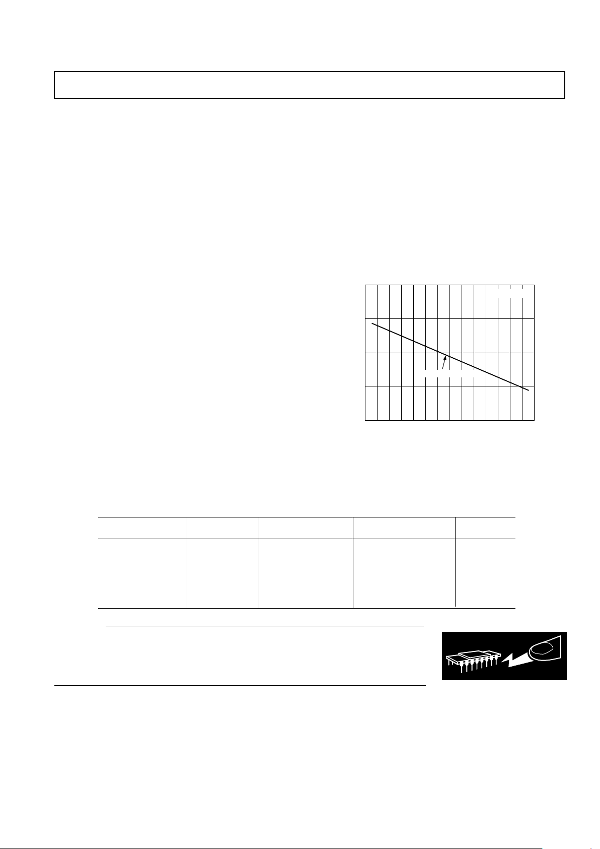
MAXIMUM POWER DISSIPATION
The maximum power that can be safely dissipated by the
AD8079 is limited by the associated rise in junction temperature. The maximum safe junction temperature for plastic
encapsulated devices is determined by the glass transition temperature of the plastic, approximately +150°C. Exceeding this
limit temporarily may cause a shift in parametric performance
due to a change in the stresses exerted on the die by the package.
Exceeding a junction temperature of +175°C for an extended
period can result in device failure.
While the AD8079 is internally short circuit protected, this
may not be sufficient to guarantee that the maximum junction
temperature (+150°C) is not exceeded under all conditions. To
ensure proper operation, it is necessary to observe the maximum
power derating curves.
MAXIMUM POWER DISSIPATION – Watts
AMBIENT TEMPERATURE – °C
2.0
1.5
0
–50 90–40 –30 –20 –10 0 10 20 30 40 50 60 70
1.0
0.5
80
TJ = +150°C
8-PIN SOIC PACKAGE
Figure 2. Plot of Maximum Power Dissipation vs.
Temperature
CAUTION
ESD (electrostatic discharge) sensitive device. Electrostatic charges as high as 4000 V readily
accumulate on the human body and test equipment and can discharge without detection.
Although the AD8079 features proprietary ESD protection circuitry, permanent damage may
occur on devices subjected to high energy electrostatic discharges. Therefore, proper ESD
precautions are recommended to avoid performance degradation or loss of functionality.
WARNING!
ESD SENSITIVE DEVICE
ORDERING GUIDE
Temperature Package Package
Model Gain Range Description Option
AD8079AR G = +2.0 –40°C to +85°C 8-Pin Plastic SOIC SO-8
AD8079AR-REEL G = +2.0 –40°C to +85°C REEL SOIC SO-8
AD8079AR-REEL7 G = +2.0 –40°C to +85°C REEL 7 SOIC SO-8
AD8079BR G = +2.2 –40°C to +85°C 8-Pin Plastic SOIC SO-8
AD8079BR-REEL G = +2.2 –40°C to +85°C REEL SOIC SO-8
AD8079BR-REEL7 G = +2.2 –40°C to +85°C REEL 7 SOIC SO-8

AD8079
REV. A
–4–
FREQUENCY – Hz
1M
NORMALIZED FLATNESS – dB
1G10M 100M
–0.5
0.1
0
–0.1
–0.2
–0.3
–0.4
1
0
–9
–1
–2
–3
–4
–5
–6
–7
–8
NORMALIZED FREQUENCY RESPONSE – dB
SIDE 2
SIDE 1
SIDE 2
SIDE 1
RL = 100Ω
VIN = 50mV rms
50Ω
50Ω
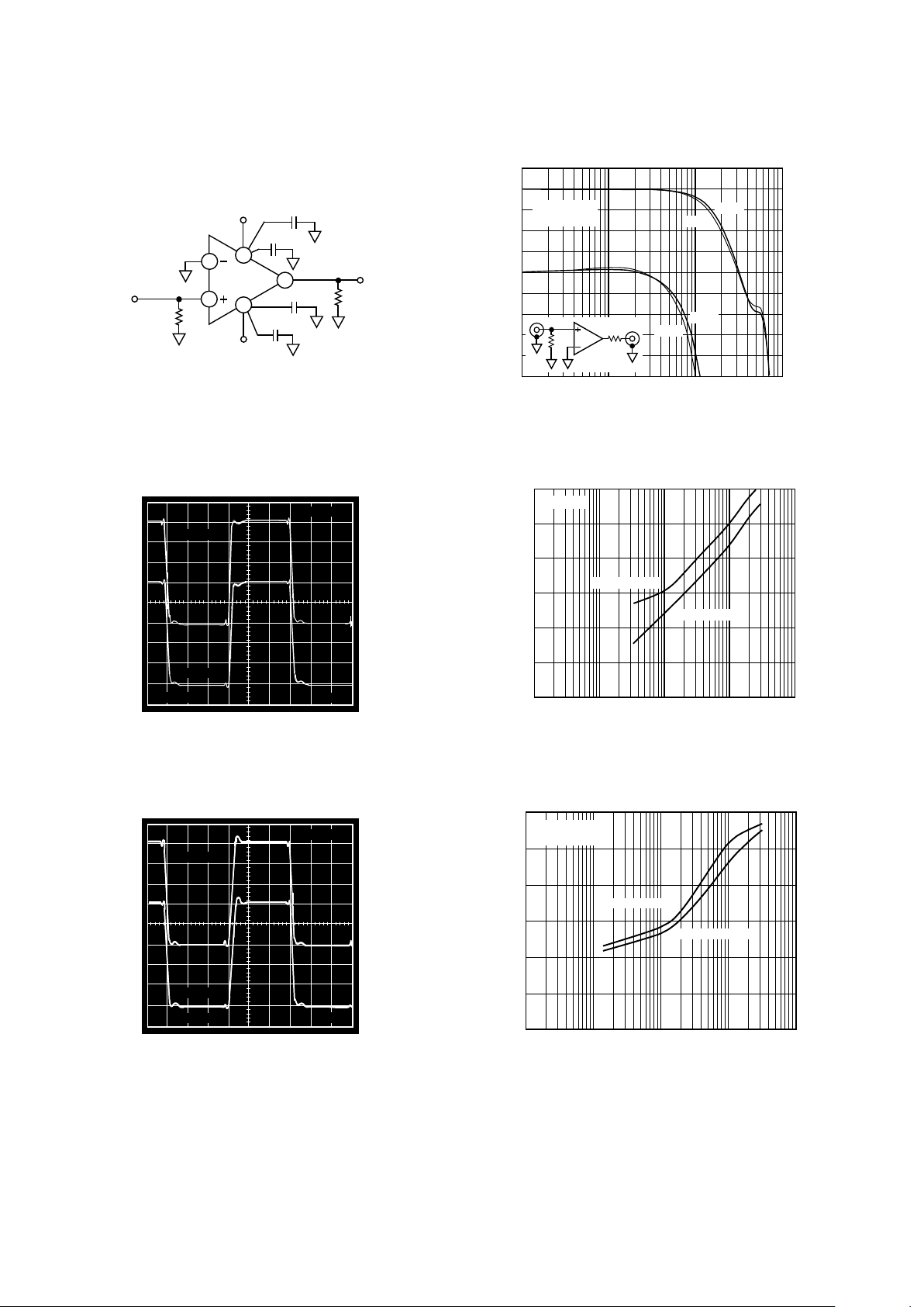
Figure 6. Frequency Response and Flatness
FREQUENCY – Hz
–50
–60
DISTORTION – dBc
–110
10k 100M100k 1M 10M
–70
–80
–100
–90
2ND HARMONIC
3RD HARMONIC
RL = 100Ω
Figure 7. Distortion vs. Frequency, RL = 100
Ω
–60
–90
–120
–100
–110
–80
–70
100k 100M10M1M10k
FREQUENCY – Hz
DISTORTION – dBc
RL = 1kΩ
V
OUT
= 2Vp-p
2ND HARMONIC
3RD HARMONIC
Figure 8. Distortion vs. Frequency, RL = 1 k
Ω
8
7
6
2
1
AD8079
+5V
10µF
0.1µF
50Ω
V
IN
PULSE
GENERATOR
0.1µF
10µF
–5V
R
L
= 100Ω
TR/TF = 250ps
Figure 3. Test Circuit
20mV
5ns
SIDE 2
SIDE 1
100mV STEP
Figure 4. 100 mV Step Response
200mV
5ns
SIDE 2
SIDE 1
1V STEP
Figure 5. 1 V Step Response
 Loading...