Analog Devices AD8074 5 a Datasheet

500 MHz, G = +1 and +2 Triple
a
FEATURES
Dual Supply ⴞ5 V
High-Speed Fully Buffered Inputs and Outputs
600 MHz Bandwidth (–3 dB) 200 mV p-p
500 MHz Bandwidth (–3 dB) 2 V p-p
1600 V/s Slew Rate, G = +1
1350 V/s Slew Rate, G = +2
Fast Settling Time: 4 ns
Low Supply Current: <30 mA
Excellent Video Specifications (R
Gain Flatness of 0.1 dB to 50 MHz
0.01% Differential Gain Error
0.01ⴗ Differential Phase Error
“All Hostile“ Crosstalk
–80 dB @ 10 MHz
–50 dB @ 100 MHz
High “OFF” Isolation of 90 dB @ 10 MHz
Low Cost
Fast Output Disable Feature
APPLICATIONS
RGB Buffer in LCD and Plasma Displays
RGB Driver
Video Routers
= 150 ⍀):
L
Video Buffers with Disable
AD8074/AD8075
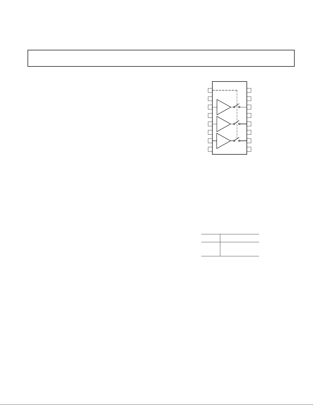
FUNCTIONAL BLOCK DIAGRAM
AD8074 /AD8075
OE
DGND
IN2
AGND
IN1
AGND
IN0
V
1
2
G =
3
+1/+2
4
G =
5
+1/+2
6
G =
7
+1/+2
8
EE
V
16
CC
V
15
CC
14
OUT2
13
V
EE
12
OUT1
V
11
CC
OUT0
10
V
9
EE
PRODUCT DESCRIPTION
The AD8074/AD8075 are high-speed triple video buffers with
G = +1 and +2 respectively. They have a –3 dB full signal bandwidth in excess of 450 MHz, along with slew rates in excess of
1400 V/µs. With better than –80 dB of all hostile crosstalk and
90 dB isolation, they are useful in many high-speed applications. The differential gain and differential phase error are 0.01%
and 0.01°. Gain flatness of 0.1 dB up to 50 MHz makes the
AD8074/AD8075 ideal for RGB buffering or driving. They
consume less than 30 mA on a ±5 V supply.
Both devices offer a high-speed disable feature that allows the
outputs to be put into a high impedance state. This allows the
building of larger input arrays while minimizing “OFF” channel output loading. The AD8074/AD8075 are offered in a
16-lead TSSOP package.
REV. A
Information furnished by Analog Devices is believed to be accurate and
reliable. However, no responsibility is assumed by Analog Devices for its
use, nor for any infringements of patents or other rights of third parties that
may result from its use. No license is granted by implication or otherwise
under any patent or patent rights of Analog Devices.
Table I. Truth Table
OE OUT0, 1, 2
0 IN0, IN1, IN2
1 High Z
One Technology Way, P.O. Box 9106, Norwood, MA 02062-9106, U.S.A.
Tel: 781/329-4700 www.analog.com
Fax: 781/326-8703 © Analog Devices, Inc., 2001

AD8074/AD8075–SPECIFICATIONS
(TA = 25ⴗC, VS = ⴞ5 V, unless otherwise noted.)
Parameter Conditions Min Typ Max Unit
DYNAMIC PERFORMANCE
–3 dB Bandwidth (Small Signal) V
–3 dB Bandwidth (Large Signal) V
0.1 dB Bandwidth V
Slew Rate 2 V Step, R
= 200 mV p-p, CL = 5 pF 330/310 600/550 MHz
IN
V
= 200 mV p-p, RL = 150 Ω 250/230 400/400 MHz
IN
= 2 V p-p, CL = 5 pF 330/300 500/500 MHz
IN
V
= 2 V p-p, RL = 150 Ω 250/230 350/350 MHz
IN
= 200 mV p-p, CL = 5 pF 70/65 MHz
IN
V
= 200 mV p-p, RL = 150 Ω 70/65 MHz
IN
= 1 kΩ/150 Ω 1600/1350 V/µs
L
Settling Time to 0.1% 2 V Step, RL = 1 kΩ/150 Ω 4/7.5 ns
NOISE/DISTORTION PERFORMANCE
Differential Gain V = 3.58 MHz, 150 Ω 0.01 %
Differential Phase V = 3.58 MHz, 150 Ω 0.01 Degrees
All Hostile Crosstalk V = 10 MHz, R
V = 100 MHz, R
OFF Isolation V = 10 MHz, R
= 1 kΩ –80/–74 dB
L
= 1 kΩ –50/–44 dB
L
= 150 Ω 90 dB
L
Voltage Noise V = 10 kHz to 100 MHz 19.5/22 nV/√Hz
DC PERFORMANCE
Voltage Gain Error No Load ±0.1/±0.2 ±0.15/± 0.65 %
Input Offset Voltage 2.5 27/40 mV
to T
T
MIN
MAX
3mV
Input Offset Drift 10 µV/°C
Input Bias Current 5 9.5/10 µA
INPUT CHARACTERISTICS
Input Resistance 10 MΩ
Input Capacitance Channel Enabled 1.5 pF
Channel Disabled 1.5 pF
Input Voltage Range ±2.8/±1.4 V
OUTPUT CHARACTERISTICS
Output Voltage Swing R
= 1 kΩ +VS – 1.95 +VS – 1.8 V
L
R
= 150 Ω +VS – 2.35 +VS – 2.2 V
L
+ 2.1 –VS + 1.8 V
–V
S
+ 2.30 –VS + 2.2 V
–V
S
Short Circuit Current (Protected) 70 mA
Output Resistance Enabled 0.5 Ω
Disabled 3.5 7.5 MΩ
Output Capacitance Disabled 2.2 pF
POWER SUPPLY
Operating Range ±4.5 ±5.5 V
Power Supply Rejection Ratio +PSRR: +V
–PSRR: –V
= +4.5 V to +5.5 V, –VS = –5 V 60 74 dB
S
= –4.5 V to –5.5 V, +VS = +5 V 56 64 dB
S
Quiescent Current All Channels “ON” 21.5/24 30 mA
All Channels “OFF” 3/4 5.5 mA
T
MIN
to T
MAX
23/26 mA
DIGITAL INPUT
Logic “1” Voltage OE Input 2.0 V
Logic “0” Voltage OE Input 0.8 V
Logic “1” Input Current OE = 4 V 100 nA
Logic “0” Input Current OE = 0.4 V 1 µA
OPERATING TEMPERATURE RANGE
Temperature Range Operating (Still Air) –40 +85 °C
θ
JA
θ
JC
Specifications subject to change without notice.
Operating (Still Air) 150.4 °C/W
Operating 27.6 °C/W
–2–
REV. A

AD8074/AD8075
AMBIENT TEMPERATURE – ⴗC
MAXIMUM POWER DISSIPATION – Watts
TJ = 150ⴗC
010 30 50
70
90
0
0.5
1.0
1.5
–50 –30 –10
ABSOLUTE MAXIMUM RATINGS
Supply Voltage . . . . . . . . . . . . . . . . . . . . . . . . . . . . . . . . . 12.0 V
Internal Power Dissipation
2, 3
1
AD8074/AD8075 16-Lead TSSOP (RU) . . . . . . . . . . . . . 1 W
Input Voltage
IN0, IN1, IN2 . . . . . . . . . . . . . . . . . . . . . . . . . VEE ≤ VIN ≤ V
OE . . . . . . . . . . . . . . . . . . . . . . . . . . . . . DGND ≤ VIN ≤ V
Output Short Circuit Duration . . . . . . . . . . . . . . . . . . Indefinite
CC
CC
3
Storage Temperature Range . . . . . . . . . . . . . . –65°C to +150°C
Lead Temperature Range (Soldering 10 sec) . . . . . . . . . . . 300°C
NOTES
1
Stresses above those listed under Absolute Maximum Ratings may cause permanent damage to the device. This is a stress rating only; functional operation of the
device at these or any other conditions above those indicated in the operational
section of this specification is not implied. Exposure to absolute maximum rating
conditions for extended periods may affect device reliability.
2
Specification is for device in free air (TA = 25°C).
3
16-lead plastic TSSOP; θJA = 150.4°C/W. Maximum internal power dissipation (P
) should be derated for ambient temperature (TA) such that
D
PD < (150°C – TA)/θJA.
ORDERING GUIDE
Temperature Package Package
Model Range Description Option
AD8074ARU –40°C to +85°C 16-Lead Plastic TSSOP RU-16
AD8075ARU –40°C to +85°C 16-Lead Plastic TSSOP RU-16
AD8074-EVAL Evaluation Board
AD8075-EVAL Evaluation Board
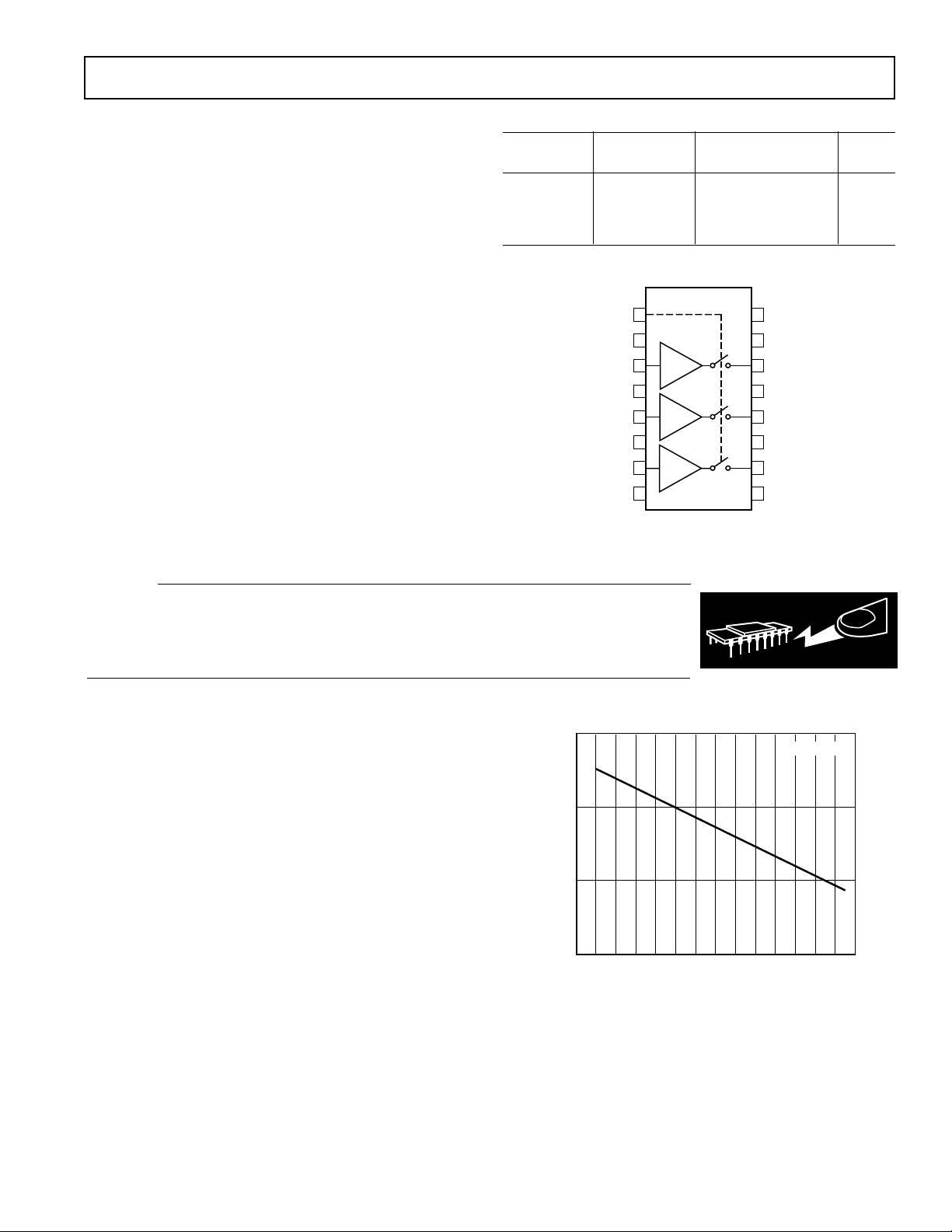
PIN CONFIGURATION
AD8074 /AD8075
OE
DGND
IN2
AGND
IN1
AGND
IN0
V
1
2
G =
3
+1/+2
4
G =
5
+1/+2
6
G =
7
+1/+2
8
EE
V
16
CC
V
15
CC
14
OUT2
13
V
EE
12
OUT1
V
11
CC
OUT0
10
V
9
EE
CAUTION
ESD (electrostatic discharge) sensitive device. Electrostatic charges as high as 4000 V readily
accumulate on the human body and test equipment and can discharge without detection. Although
the AD8074/AD8075 features proprietary ESD protection circuitry, permanent damage may occur
on devices subjected to high-energy electrostatic discharges. Therefore, proper ESD precautions
are recommended to avoid performance degradation or loss of functionality.
MAXIMUM POWER DISSIPATION
The maximum power that can be safely dissipated by the AD8074/
AD8075 is limited by the associated rise in junction temperature.
The maximum safe junction temperature for plastic encapsulated
devices is determined by the glass transition temperature of the
plastic, approximately 150°C. Temporarily exceeding this limit
may cause a shift in parametric performance due to a change in
the stresses exerted on the die by the package. Exceeding a junction temperature of 175°C for an extended period can result in
device failure.
While the AD8074/AD8075 is internally short circuit protected,
this may not be sufficient to guarantee that the maximum junction
temperature (150°C) is not exceeded under all conditions. To
ensure proper operation, it is necessary to observe the maximum
power derating curves shown in Figure 1.
Figure 1. Maximum Power Dissipation vs. Temperature
WARNING!
ESD SENSITIVE DEVICE
REV. A
–3–

AD8074/AD8075–Typical Performance Characteristics
FLATNESS
GAIN
2V p-p
200mV p-p
2V p-p
FREQUENCY – MHz
0.1 10001 10 100
1
0
–1
–2
–3
–4
–5
–6
–7
–8
–9
0.4
0.3
0.2
0.1
0
–0.1
–0.2
–0.3
–0.4
–0.5
–0.6
NORMALIZED FLATNESS – dB
NORMALIZED GAIN – dB
0.1 10001 10 100
2
1
0
–1
–2
–3
–4
–5
–6
–7
–8
–9
–10
0.6
0.5
0.4
0.3
0.2
0.1
0
–0.1
–0.2
–0.3
–0.4
–0.5
–0.6
2V p-p
GAIN
FLATNESS
NORMALIZED FLATNESS – dB
NORMALIZED GAIN – dB
200mV p-p
FREQUENCY – MHz
2V p-p
1
GAIN
0
–1
–2
FLATNESS
–3
–4
GAIN – dB
–5
–6
–7
–8
–9
0.1 10001 10 100
FREQUENCY – MHz
200mV p-p
2V p-p
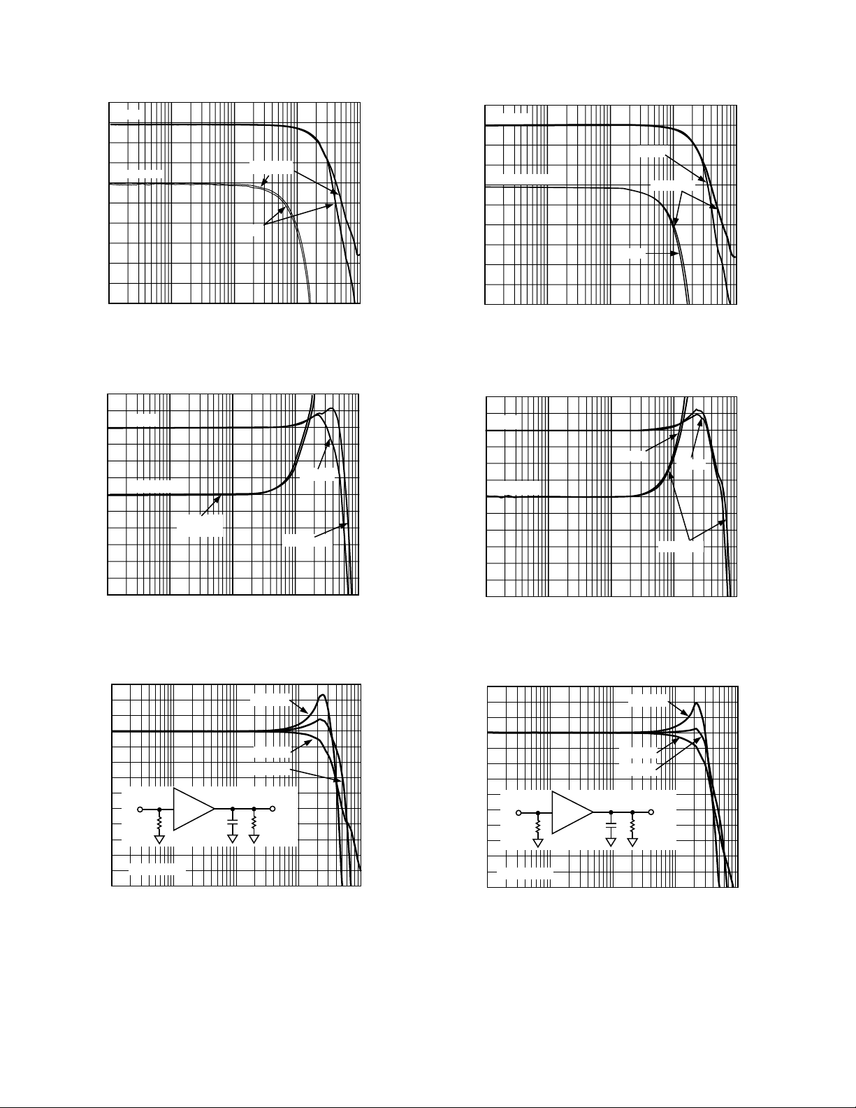
TPC 1. AD8074 Frequency Response; RL = 150
2
1
GAIN
0
–1
–2
–3
FLATNESS
–4
–5
GAIN – dB
–6
–7
–8
–9
–10
0.1 10001 10 100
200mV p-p
2V p-p
FREQUENCY – MHz
2V p-p
200mV p-p
0.4
0.3
0.2
0.1
0
–0.1
–0.2
–0.3
–0.4
–0.5
–0.6
Ω
0.6
0.5
0.4
0.3
0.2
0.1
0
–0.1
–0.2
–0.3
–0.4
–0.5
–0.6
FLATNESS – dB
FLATNESS – dB
TPC 4. AD8075 Frequency Response; RL = 150
Ω
TPC 2. AD8074 Frequency Response; RL = 1 kΩ, CL = 5 pF
3
2
1
0
–1
–2
–3
–4
GAIN – dB
V
–5
IN
75
–6
–7
–8
TPC 3. AD8074 Frequency Response vs. Capacitive Load
–9
–10
0.1 1 10 100 1000
⍀
V
= 2V p-p
OUT
CL = 10pF
CL = 0pF
CL = 5pF
C
FREQUENCY – MHz
L
1k
TPC 5. AD8075 Frequency Response; RL = 1 kΩ, CL = 5 pF
3
2
1
0
–1
–2
–3
–4
V
OUT
⍀
–4–
–5
V
IN
NORMALIZED GAIN – dB
–10
–6
–7
–8
–9
75⍀
V
= 2V p-p
OUT
0.1 1 10 100 1000
FREQUENCY – MHz
TPC 6. AD8075 Frequency Response vs. Capacitive Load
CL = 10pF
CL = 0pF
CL = 5pF
V
C
L
150k⍀
OUT
REV. A

0
FREQUENCY – MHz
0
0.1 1000
1 10 100
–10
–20
–30
–40
–50
–60
–70
–80
–90
–100
–110
V
OUT
= 2V p-p (ACTIVE CHANNEL(s))
R
L
= 150⍀
R
T
= 37.5⍀
ALL-HOSTILE
ADJACENT
CROSSTALK – dB
V
= 2V p-p (ACTIVE CHANNEL(s))
OUT
–10
= 1k⍀
R
L
= 37.5⍀
R
T
–20
–30
–40
–50
–60
ALL-HOSTILE
ADJACENT
1 10 100
FREQUENCY – MHz
–70
CROSSTALK – dB
–80
–90
–100
–110
0.1 1000
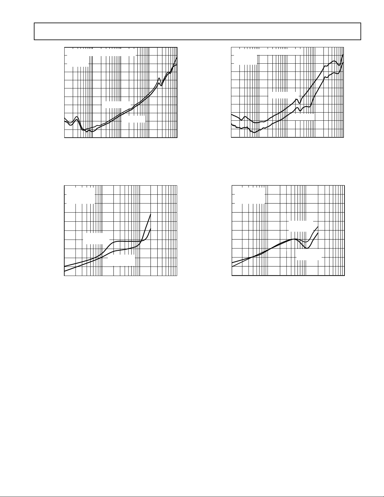
TPC 7. AD8074 Crosstalk vs. Frequency (All Hostile and
Adjacent R
= 1 kΩ)
L
AD8074/AD8075
TPC 9. AD8075 Crosstalk vs. Frequency (All Hostile and
Adjacent R
= 150 Ω)
L
0
V
= 2V p-p
OUT
–10
= 150⍀
R
L
= 37.5⍀
R
T
–20
–30
–40
–50
–60
DISTORTION – dBc
–70
–80
–90
–100
1 100010 100
SECOND
HARMONIC
THIRD
HARMONIC
FUNDAMENTAL FREQUENCY – MHz
TPC 8. AD8074 Distortion vs. Frequency
0
V
= 2V p-p
OUT
–10
–20
–30
–40
–50
–60
DISTORTION – dBc
–70
–80
–90
–100
= 150⍀
R
L
= 37.5⍀
R
T
SECOND
HARMONIC
THIRD
HARMONIC
1 100010 100
FUNDAMENTAL FREQUENCY – MHz
TPC 10. AD8075 Distortion vs. Frequency
REV. A
–5–
 Loading...