High Gain Bandwidth Product
FEATURES
• FET input amplifier: 0.6 pA input bias current
• Stable for gains ≥8
• High speed
• 54 MHz, –3 dB bandwidth (G = +10)
• 640 V/µs slew rate
• Low noise
• 6.6 nV/√Hz
• 0.6 fA/√Hz
• Low offset voltage (1.0 mV max)
• Wide supply voltage range: 5 V to 24 V
• No phase reversal
• Low input capacitance
• Single-supply and rail-to-rail output
• Excellent distortion specs: SFDR 95 dBc @ 1 MHz
• High common-mode rejection ratio: –106 dB
• Low power: 6.5 mA typical supply current
• Low cost
• Small packaging: SOT-23-5
APPLICATIONS
• Photodiode preamplifier
• Precision high gain amplifier
• High gain, high bandwidth composite amplifier
GENERAL DESCRIPTION
The AD8067 Fast FET amp is a voltage feedback amplifier with
FET inputs offering wide bandwidth (54 MHz @ G = +10) and high
slew rate (640 V/µs). The AD8067 is fabricated in a proprietary,
dielectrically isolated eXtra Fast Complementary Bipolar process
(XFCB) that enables high speed, low power, and high performance
FET input amplifiers.
The AD8067 is designed to work in applications that require high
speed and low input bias current, such as fast photodiode
preamplifiers. As required by photodiode applications, the laser
trimmed AD8067 has excellent dc voltage offset (1.0 mV max)
and drift (15 µV/°C max).
Rev. 0
Information furnished by Analog Devices is believed to be accurate and reliable.
However, no responsibility is assumed by Analog Devices for its use, nor for any
infringements of patents or other rights of third parties that may result from its use.
Specifications subject to change without notice. No license is granted by implication
or otherwise under any patent or patent rights of Anal og Devices. Trademarks and
registered trademarks are the property of their respective companies.
Precision Fast FET
™
Op Amp
AD8067
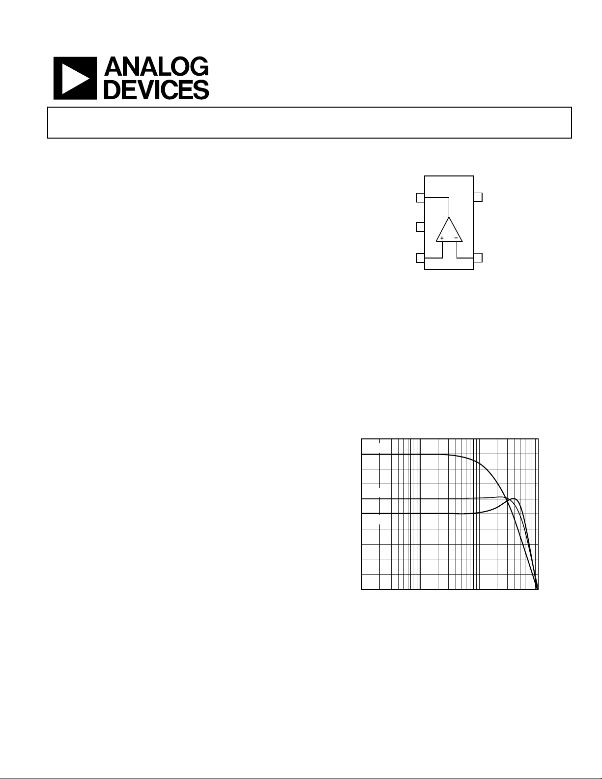
CONNECTION DIAGRAM
SOT-23-5 (RT-5)
+V
V
1
OUT
2
–V
S
3
+IN
Figure 1. Connection Diagram (Top View)
The FET input bias current (5 pA max) and low voltage noise
(6.6 nV/√Hz) also contribute to making it appropriate for precision
applications. With a wide supply voltage range (5 V to 24 V) and
rail-to-rail output, the AD8067 is well suited to a variety of
applications that require wide dynamic range and low distortion.
The AD8067 amplifier consumes only 6.5 mA of supply current,
while capable of delivering 30 mA of load current and driving
capacitive loads of 100 pF. The AD8067 amplifier is available in a
SOT-23-5 package and is rated to operate over the industrial
temperature range, –40°C to +85°C.
28
G = +20
26
24
22
G = +10
20
18
G = +8
GAIN – dB
16
14
12
10
8
0.1 1 10 100
Figure 2. Small Signal Frequency Respon se
One Technology Way, P.O. Box 9106, Norwood, MA 02062-9106, U.S.A.
Tel: 781.329.4700 www.analog.com
Fax: 781.326.8703 © 2002 Analog Devices, Inc. All rights reserved.
FREQUENCY – MHz
5
S
4
–IN

AD8067
TABLE OF CONTENTS
AD8067–Specifications for ±5 V...........................................................4
Input Protection ................................................................................18
AD8067–Specifications for +5 V...........................................................5
AD8067–Specifications for ±12 V.........................................................6
Absolute Maximum Ratings ..................................................................7
Maximum Power Dissipation............................................................7
Typical Performance Characteristics .................................................... 8
Test Circuits............................................................................................13
Theory of Operation .............................................................................15
Basic Frequency Response............................................................... 15
Resistor Selection for Wideband Operation..................................16
Input and Output Overload Behavior............................................17
TABLES
Table 1. Recommended Values of RG and RF.....................................15
Table 2. RMS Noise Contributions of Photodiode Preamp............. 20
REVISION HISTORY
Revision 0: Initial Version
Capacitive Load Drive ......................................................................18
Layout, Grounding, and Bypassing Considerations.....................18
Applications............................................................................................20
Wideband Photodiode Preamp.......................................................20
Using the AD8067 at Gains of Less Than 8...................................21
Single-Supply Operation..................................................................22
High Gain, High Bandwidth Composite Amplifier......................22
Outline Dimensions ..............................................................................24
Ordering Guide .................................................................................24
Table 3. Ordering Guide........................................................................24
Rev. 0 | Page 2 of 24

AD8067
FIGURES
Figure 1. Connection Diagram (Top View)..........................................1
Figure 32. Output Saturation Voltage vs. Temperature.................... 12
Figure 2. Small Signal Frequency Response.........................................1
Figure 3. Maximum Power Dissipation vs. Temperature for
a 4-Layer Board ...............................................................................7
Figure 4. Small Signal Frequency Response for Various Gains .........8
Figure 5. Small Signal Frequency Response for Various Supplies.....8
Figure 6. Large Signal Frequency Response for Various Supplies.....8
Figure 7. 0.1 dB Flatness Frequency Response ...................................8
Figure 8. Small Signal Frequency Response for Various C
Figure 9. Frequency Response for Various Output Amplitudes........8
Figure 10. Small Signal Frequency Response for Various RF.............9
Figure 11. Distortion vs. Frequency for Various Loads ......................9
Figure 12. Distortion vs. Frequency for Various Amplitudes.............9
Figure 13. Open-Loop Gain and Phase ................................................9
Figure 14. Distortion vs. Frequency for Various Supplies..................9
Figure 15. Distortion vs. Output Amplitude for Various Loads ........9
Figure 16. Small Signal Transient Response 5 V Supply...................10
Figure 17. Output Overdrive Recovery...............................................10
LOAD
.........8
Figure 33. Open-Loop Gain vs. Load Current for Various
Supplies.......................................................................................... 12
Figure 34. Standard Test Circuit.......................................................... 13
Figure 35. Open-Loop Gain Test Circuit........................................... 13
Figure 36. Test Circuit for Capacitive Load....................................... 13
Figure 37. CMRR Test Circuit ............................................................. 14
Figure 38. Positive PSRR Test Circuit................................................. 14
Figure 39. Output Impedance Test Circuit ........................................ 14
Figure 40. Noninverting Gain Configuration................................... 15
Figure 41. Open-Loop Frequency Response.................................... 15
Figure 42. Inverting Gain Configuration........................................... 15
Figure 43. Input and Board Capacitances.......................................... 16
Figure 44. Op Amp DC Error Sources.............................................. 17
Figure 45. Simplified Input Schematic............................................. 17
Figure 46 Current Limiting Resistor .................................................. 18
Figure 47. Guard-Ring Configurations.............................................. 18
Figure 48. Guard-Ring Layout SOT-23-5 .......................................... 18
Figure 18. Long-Term Settling Time...................................................10
Figure 19. Small Signal Transient Response ± 5 V Supply ...............10
Figure 20. Large Signal Transient Response.......................................10
Figure 21. 0.1% Short-Term Settling Time........................................10
Figure 22. Input Bias Current vs. Temperature..................................11
Figure 23. Input Offset Voltage Histogram ........................................11
Figure 24. Voltage Noise........................................................................11
Figure 25. Input Bias Current vs. Common-Mode Voltage..............11
Figure 26. Input Offset Voltage vs. Common-Mode Voltage...........11
Figure 27. CMRR vs. Frequency ..........................................................11
Figure 28. Output Impedance vs. Frequency .....................................12
Figure 29. Output Saturation Voltage vs. Output Load Current......12
Figure 30. PSRR vs. Frequency.............................................................12
Figure 31. Quiescent Current vs. Temperature for Various
Supply Voltages..............................................................................12
Figure 49. Wideband Photodiode Preamp......................................... 20
Figure 50. Photodiode Voltage Noise Contributions ....................... 20
Figure 51. Photodiode Preamplifier ................................................... 21
Figure 52. Photodiode Preamplifier Frequency Response .............. 21
Figure 53. Photodiode Preamplifier Pulse Response....................... 21
Figure 54. Gain of Less than 2 Schematic .......................................... 21
Figure 55. Gain of 2 Pulse Response .................................................. 22
Figure 56. Single-Supply Operation Schematic ................................ 22
Figure 57. AD8067/AD8009 Composite ........................................... 23
Figure 58. Gain Bandwidth Response ................................................ 23
Figure 59. Large Signal Response........................................................ 23
Figure 60. Small Signal Response........................................................ 23
Figure 61. 5-Lead Plastic Surface Mount Package ........................... 24
Rev. 0 | Page 3 of 24
AD8067
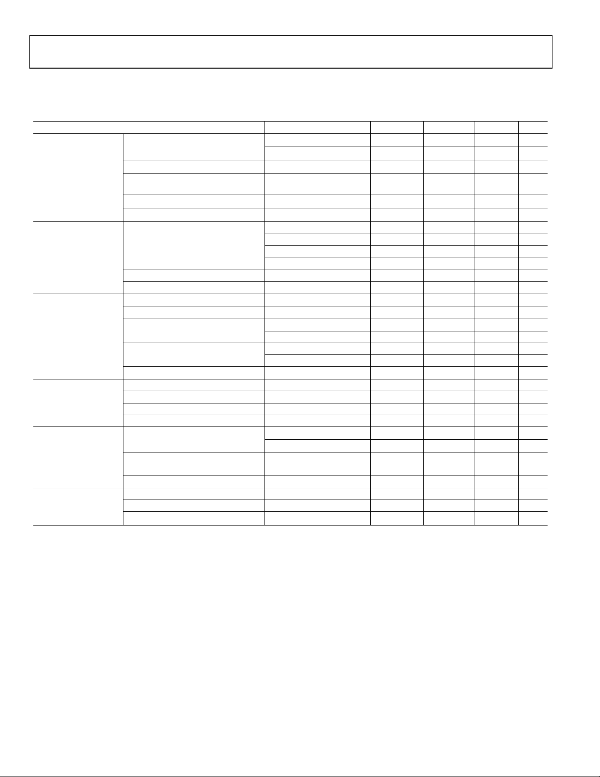
AD8067–SPECIFICATIONS FOR ±5 V
VS = ±5 V (@ T
= +25°C, G = +10, RF = RL =1 kΩ, Unless Otherwise Noted.)
A
Parameter Conditions Min Typ Max Unit
= 0.2 V p-p
DYNAMIC
PERFORMANCE
–3 dB Bandwidth
Bandwidth for 0.1 dB Flatness
Output Overdrive Recovery Time
(Pos/Neg)
Slew Rate
Settling Time to 0.1%
V
O
= 2 V p-p
V
O
V
= 0.2 V p-p
O
= ±0.6 V
V
I
V
= 5 V Step
O
= 5 V Step
V
O
39 54 MHz
54 MHz
8 MHz
115/190 ns
500 640 V/µs
27 ns
fC = 1 MHz, 2 V p-p 95 dBc
fC = 1 MHz, 8 V p-p 84 dBc
fC = 5 MHz, 2 V p-p 82 dBc
= 1 MHz, 2 V p-p, RL = 150 Ω
f
C
72 dBc
NOISE/DISTORTION
PERFORMANCE
Spurious Free Dynamic Range (SFDR)
Input Voltage Noise f = 10 kHz 6.6 nV/√Hz
Input Current Noise f = 10 kHz 0.6 fA/√Hz
DC PERFORMANCE
Input Offset Voltage
Input Offset Voltage Drift
Input Bias Current
Input Offset Current
Open-Loop Gain
0.6 5 pA
to T
T
MIN
25 pA
MAX
0.2 1 pA
T
to T
MIN
V
O
1 pA
MAX
= ±3 V
0.2 1.0 mV
1 15 µV/°C
103 119 dB
Common-Mode Input Impedance 1000||1.5 GΩ||pF
INPUT
CHARACTERISTICS
OUTPUT
CHARACTERISTICS
Differential Input Impedance 1000||2.5 GΩ||pF
Input Common-Mode Voltage Range –5.0 2.0 V
Common-Mode Rejection Ratio (CMRR) V
Output Voltage Swing
= –1 V to +1 V –85 –106 dB
CM
RL = 1 kΩ –4.86 to +4.83
= 150 Ω
R
L
–4.92 to +4.92 V
–4.67 to +4.72 V
Output Current SFDR > 60 dBc, f = 1 MHz 30 mA
Short Circuit Current 105 mA
Capacitive Load Drive 30% over shoot 120 pF
Operating Range 5 24 V
POWER SUPPLY
Quiescent Current 6.5 6.8 mA
Power Supply Rejection Ratio (PSRR) –90 –109 dB
Rev. 0 | Page 4 of 24
AD8067
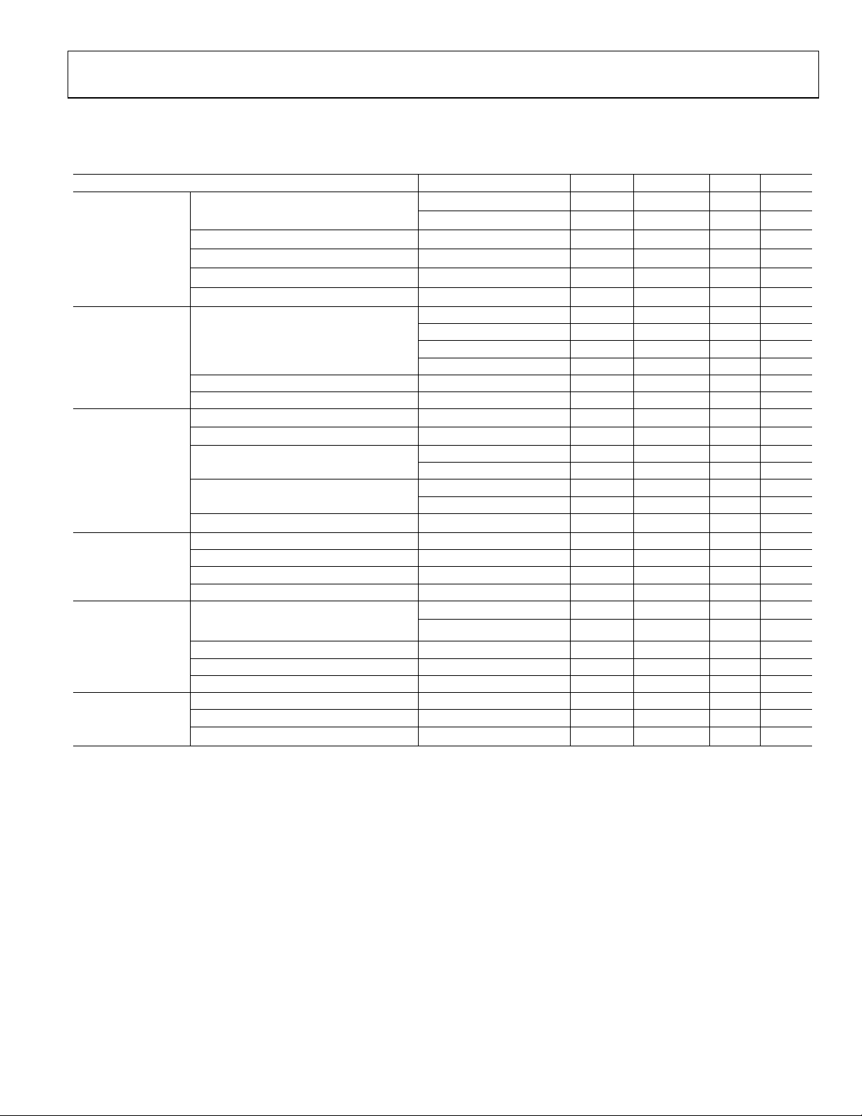
AD8067–SPECIFICATIONS FOR +5 V
VS = +5 V (@ T
= +25°C, G = +10, RL =RF = 1 kΩ, Unless Otherwise Noted.)
A
Parameter Conditions Min Typ Max Unit
V
DYNAMIC
PERFORMANCE
–3 dB Bandwidth
Bandwidth for 0.1 dB Flatness
Output Overdrive Recovery Time (Pos/Neg)
Slew Rate
Settling Time to 0.1%
= 0.2 V p-p
O
= 2 V p-p
V
O
V
= 0.2 V p-p
O
V
= +0.6 V
I
V
= 3 V Step
O
V
= 2 V Step
O
36 54 MHz
54 MHz
8 MHz
150/200 ns
390 490 V/µs
25 ns
fC = 1 MHz, 2 V p-p 86 dBc
fC = 1 MHz, 4 V p-p 74 dBc
fC = 5 MHz, 2 V p-p 60 dBc
f
= 1 MHz, 2 V p-p, RL = 150 Ω 72 dBc
C
NOISE/DISTORTION
PERFORMANCE
Spurious Free Dynamic Range (SFDR)
Input Voltage Noise f = 10 kHz 6.6 nV/√Hz
Input Current Noise f = 10 kHz 0.6 fA/√Hz
DC PERFORMANCE
Input Offset Voltage
Input Offset Voltage Drift
Input Bias Current
Input Offset Current
Open-Loop Gain
0.5 5 pA
to T
T
MIN
25 pA
MAX
0.1 1 pA
to T
T
MIN
V
O
pA
MAX
= 0.5 V to 4.5 V
0.2 1.0 mV
1 15 µV/°C
100 117 dB
Common-Mode Input Impedance 1000||2.3 GΩ||pF
INPUT
CHARACTERISTICS
OUTPUT
CHARACTERISTICS
Differential Input Impedance 1000||2.5 GΩ||pF
Input Common-Mode Voltage Range 0 2.0 V
Common-Mode Rejection Ratio (CMRR) V
Output Voltage Swing
= 0.5 Vto 1.5 V –81 –98 dB
CM
RL = 1 kΩ 0.07 to 4.89 0.03 to 4.94
=150 Ω
R
L
0.08 to 4.83
V
V
Output Current SFDR > 60 dBc, f = 1 MHz 22 mA
Short Circuit Current 95 mA
Capacitive Load Drive 30% over shoot 120 pF
Operating Range 5 24 V
POWER SUPPLY
Quiescent Current 6.4 6.7 mA
Power Supply Rejection Ratio (PSRR) –87 –103 dB
Rev. 0 | Page 5 of 24
AD8067
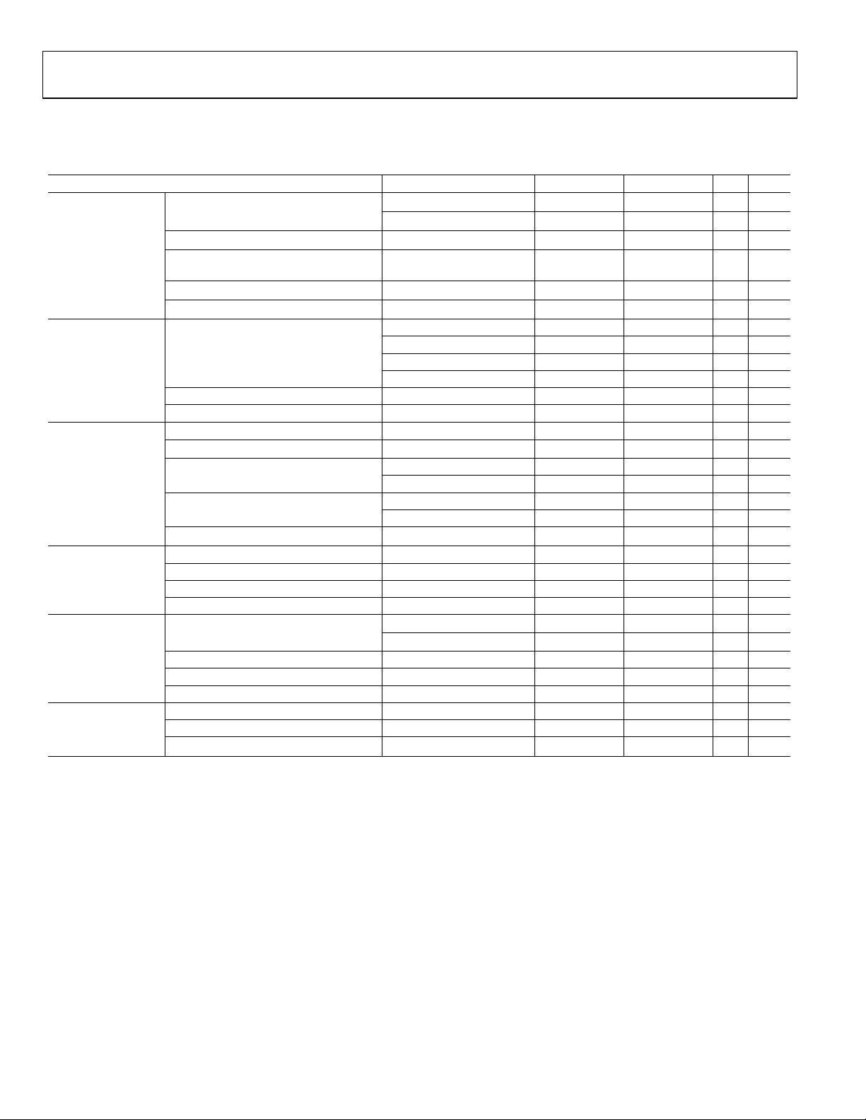
AD8067–SPECIFICATIONS FOR ±12 V
VS = ±12 V (@ T
= +25°C, G = +10, RL = RF = 1 kΩ, Unless Otherwise Noted.)
A
Parameter Conditions Min Typ Max Unit
V
DYNAMIC
PERFORMANCE
–3 dB Bandwidth
Bandwidth for 0.1 dB Flatness
Output Overdrive Recovery Time
(Pos/Neg)
Slew Rate
Settling Time to 0.1%
= 0.2 V p-p
O
= 2 V p-p
V
O
V
= 0.2 V p-p
O
= ±1.5 V 75/180 ns
V
I
V
= 5 V Step
O
= 5 V Step
V
O
39 54 MHz
53 MHz
8 MHz
500 640 V/µs
27 ns
fC = 1 MHz, 2 V p-p 92 dBc
fC = 1 MHz, 20 V p-p 84 dBc
fC = 5 MHz, 2 V p-p 74 dBc
fC = 1 MHz, 2V p-p, RL = 150 Ω 72 dBc
NOISE/DISTORTION
PERFORMANCE
Spurious Free Dynamic Range (SFDR)
Input Voltage Noise f = 10 kHz 6.6 nV/√Hz
Input Current Noise f = 10 kHz 0.6 fA/√Hz
DC PERFORMANCE
Input Offset Voltage
Input Offset Voltage Drift
Input Bias Current
Input Offset Current
Open-Loop Gain
1.0 5 pA
to T
T
MIN
25 pA
MAX
0.2 1 pA
to T
T
MIN
V
O
pA
MAX
= ±10 V
0.2 1.0 mV
1 15 µV/°C
107 119 dB
Common-Mode Input Impedance 1000||1.5 GΩ||pF
INPUT
CHARACTERISTICS
OUTPUT
CHARACTERISTICS
Differential Input Impedance 1000||2.5 GΩ||pF
Input Common-Mode Voltage Range –12.0 9.0 V
Common-Mode Rejection Ratio (CMRR) V
Output Voltage Swing
= –1 V to +1 V –89 –108 dB
CM
RL = 1 kΩ –11.70 to +11.70
= 500 Ω
R
L
–11.85 to +11.84 V
–11.31 to +11.73 V
Output Current SFDR > 60 dBc, f = 1 MHz 26 mA
Short Circuit Current 125 mA
Capacitive Load Drive 30% over shoot 120 pF
Operating Range 5 24 V
POWER SUPPLY
Quiescent Current 6.6 7.0 mA
Power Supply Rejection Ratio (PSRR) –86 –97 dB
Rev. 0 | Page 6 of 24
AD8067
ABSOLUTE MAXIMUM RATINGS
Parameter Rating
Supply Voltage 26.4 V
Power Dissipation See Figure 3
Common-Mode Input Voltage VEE – 0.5 V to VCC + 0.5 V
Differential Input Voltage 1.8 V
Storage Temperature –65°C to +125°C
Operating Temperature Range –40°C to +85°C
Lead Temperature Range
300°C
(Soldering 10 sec)
Junction Temperature 150°C
Stresses above those listed under Absolute Maximum Ratings may cause
permanent damage to the device. This is a stress rating only and functional
operation of the device at these or any other conditions above those
indicated in the operational section of this specification is not implied.
Exposure to absolute maximum rating conditions for extended periods may
affect device reliability.
Maximum Power Dissipation
The associated raise in junction temperature (TJ) on the die limits
the maximum safe power dissipation in the AD8067 package. At
approximately 150°C, which is the glass transition temperature, the
plastic will change its properties. Even temporarily exceeding this
temperature limit may change the stresses that the package exerts
on the die, permanently shifting the parametric performance of the
AD8067. Exceeding a junction temperature of 175°C for an
extended period of time can result in changes in the silicon devices,
potentially causing failure.
If the RMS signal levels are indeterminate, then consider the worst
V
case, when
In single-supply operation with RL referenced to V
V
= VS/2.
OUT
Airflow will increase heat dissipation effectively, reducing θ
= VS/4 for RL to midsupply:
OUT
()
IVP
SSD
2
()
/V
4
S
+×=
R
L
, worst case is
S–
. In
JA
addition, more metal directly in contact with the package leads
from metal traces, through holes, ground, and power planes will
reduce the θ
.
JA
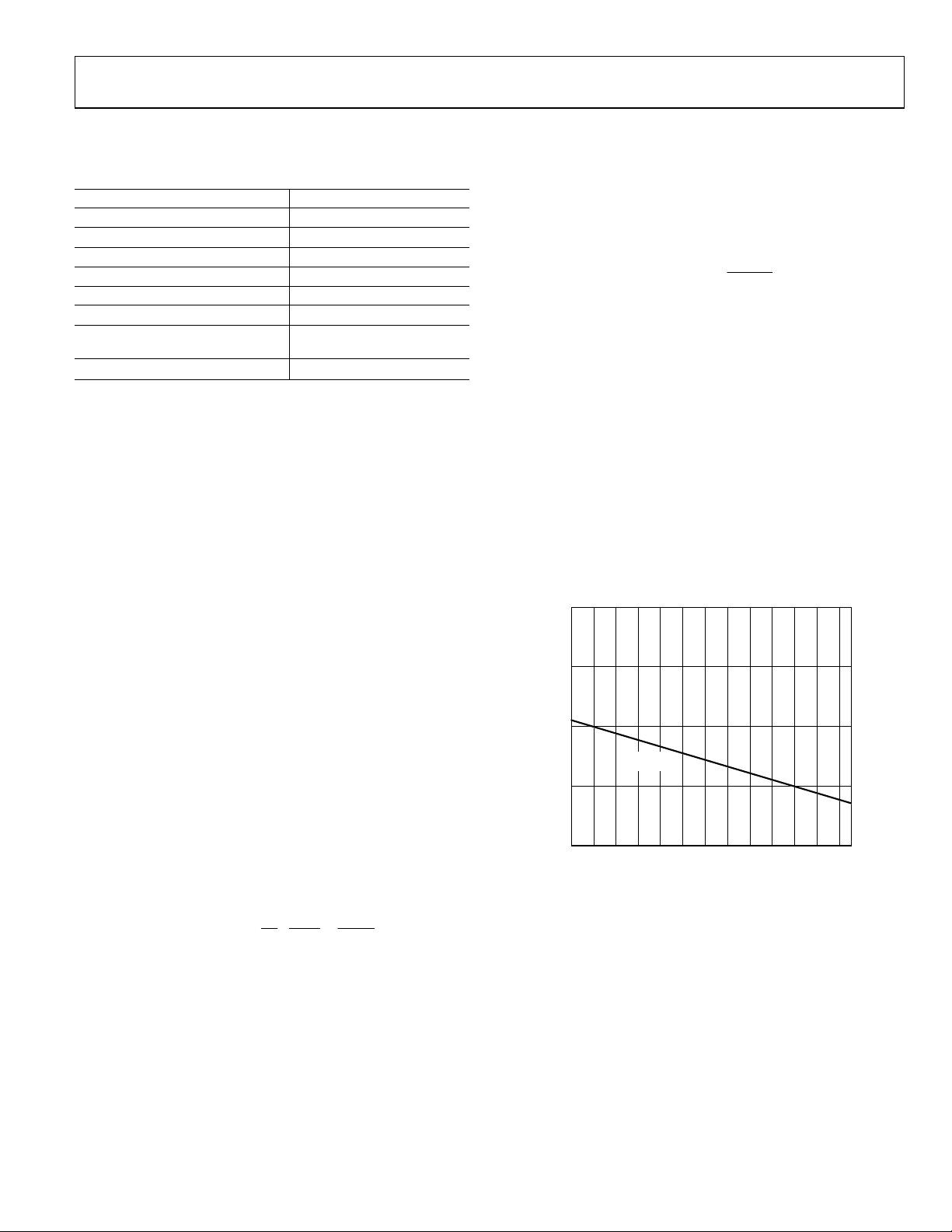
Figure 3 shows the maximum safe power dissipation in the package versus ambient temperature for the SOT-23-5 (180°C/W)
package on a JEDEC standard 4-layer board. θ
values are
JA
approximations.
It should be noted that for every 10°C rise in temperature, I
B
approximately doubles (See Figure 22).
2.0
1.5
The power dissipated in the package (P
) is the sum of the
D
quiescent power dissipation and the power dissipated in the
package due to the load drive. The quiescent power is the voltage
between the supply pins (V
) times the quiescent current (IS).
S
Assuming the load (RL) is referenced to midsupply, the total drive
power is V
and some in the load (V
/2 × I
S
, some of which is dissipated in the package
OUT
× I
OUT
). The difference between the
OUT
total drive power and the load power is the drive power dissipated
in the package. RMS output voltages should be considered.
D
If RL is referenced to V
total drive power is
V
()
+=
()
S
IVP
SSD
2
as in single-supply operation, then the
S–
× I
.
OUT
VV
×+×=
V
OUTS
R
OUT
–
L
PowerLoad–PowerDriveTotalPowerQuiescentP
2
R
L
1.0
SOT-23-5
0.5
MAXIMUM POWER DISSAPATION– W
0
–30 –20 –10 8010 20 30 40 50 60 70
–40
Figure 3. Maximum Power Dissipation vs. Temperature for a 4-Layer Board
0
AMBIENT TEMPERATURE – °C
Rev. 0 | Page 7 of 24
AD8067
TYPICAL PERFORMANCE CHARACTERISTICS
Default Conditions VS = ±5 V (@ TA = +25°C, G = +10, RL = RF = 1 kΩ, Unless Otherwise Noted.)
28
G = +20
26
24
22
G = +10
20
G = +8
18
G = +6
GAIN – dB
16
14
12
10
8
1 10 100
FREQUENCY – MHz
V
= 200mV p-p
OUT
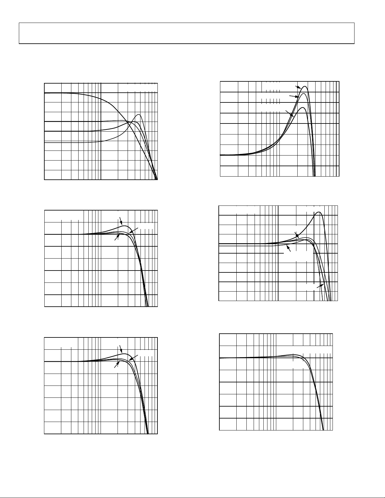
Figure 4. Small Signal Frequency Response for Various Gains
22
V
= 200mV p-p
OUT
21
20
19
18
GAIN – dB
17
16
15
14
1 10 100
FREQUENCY – MHz
V
= +5V
S
VS = ±12V
V
= ±5V
S
Figure 5. Small Signal Frequency Response for Various Supplies
22
V
= 2V p-p
OUT
21
20
19
18
GAIN – dB
17
16
15
14
1 10 100
FREQUENCY – MHz
V
= +5V
S
VS = ±12V
V
= ±5V
S
Figure 6. Large Signal Frequency Response for Various Supplies
20.7
20.6
20.5
20.4
20.3
20.2
GAIN – dB
20.1
20.0
19.9
19.8
1 10 100
V
OUT
V
= 0.7V p-p
OUT
= 1.4V p-p
V
OUT
FREQUENCY – MHz
Figure 7. 0.1 dB Flatness Frequency Response
24
V
= 200mV p-p
OUT
23
22
21
20
19
GAIN – dB
18
17
16
15
14
1 10 100
FREQUENCY – MHz
Figure 8. Small Signal Frequency Response for Various C
22
21
20
19
18
GAIN – dB
17
16
15
14
1 10 100
FREQUENCY – MHz
Figure 9. Frequency Response for Various Output Amplitudes
= 0.2V p-p
CL = 25pF
CL = 100pF
R
SNUB
V
V
= 4V p-p
OUT
CL = 100pF
= 24.9Ω
CL = 5pF
= 0.2V p-p, 2V p-p
OUT
LOAD
Rev. 0 | Page 8 of 24
 Loading...