Analog Devices AD8065 6 e Datasheet
High Performance, 145 MHz
V
FEATURES
FET input amplifier
1 pA input bias current
Low cost
High speed: 145 MHz, −3 dB bandwidth (G = +1)
180 V/µs slew rate (G = +2)
Low noise
7 nV/√Hz (f = 10 kHz)
0.6 fA/√Hz (f = 10 kHz)
Wide supply voltage range: 5 V to 24 V
Single-supply and rail-to-rail output
Low offset voltage 1.5 mV max
High common-mode rejection ratio: −100 dB
Excellent distortion specifications
SFDR −88 dB @ 1 MHz
Low power: 6.4 mA/amplifier typical supply current
No phase reversal
Small packaging: SOIC-8, SOT-23-5, and MSOP
GENERAL DESCRIPTION
APPLICATIONS
Instrumentation
Photodiode preamps
Filters
A/D drivers
Level shifting
Buffering
CONNECTION DIAGRAMS
AD8065
1
OUT
–V
2
S
3
+IN
TOP VIEW
(Not to Scale)
V
OUT1
Fast
FET™ Op Amps
AD8065/AD8066
+V
5
S
4
–IN
AD8066
1
2
–IN1
3
+IN1 –IN2
–V
4
S
TOP VIEW
(Not to Scale)
Figure 1.
1
NC
27
–IN
3
+IN
–V
4
S
(Not to Scale)
8
+V
7
V
6
5
+IN2
AD8065
TOP VIEW
S
OUT2
8
NC
+V
S
6
V
OUT
NC
5
02916-E-001
The AD8065/AD80661 FastFET amplifiers are voltage feedback
amplifiers with FET inputs offering high performance and ease
of use. The AD8065 is a single amplifier, and the AD8066 is a
dual amplifier. These amplifiers are developed in the Analog
Devices, Inc. proprietary XFCB process and allow exceptionally
low noise operation (7.0 nV/√Hz and 0.6 fA/√Hz) as well as
very high input impedance.
With a wide supply voltage range from 5 V to 24 V, the ability to
operate on single supplies, and a bandwidth of 145 MHz, the
AD8065/AD8066 are designed to work in a variety of
applications. For added versatility, the amplifiers also contain
rail-to-rail outputs.
Despite the low cost, the amplifiers provide excellent overall
performance. The differential gain and phase errors of 0.02%
and 0.02°, respectively, along with 0.1 dB flatness out to 7 MHz,
make these amplifiers ideal for video applications. Additionally,
they offer a high slew rate of 180 V/µs, excellent distortion
(SFDR of −88 dB @ 1 MHz), extremely high common-mode
rejection of −100 dB, and a low input offset voltage of 1.5 mV
maximum under warmed up conditions. The AD8065/AD8066
1
Protected by U. S. Patent No. 6,262,633.
Rev. E
Information furnished by Analog Devices is believed to be accurate and reliable.
However, no responsibility is assumed by Analog Devices for its use, nor for any
infringements of patents or other rights of third parties that may result from its use.
Specifications subject to change without notice. No license is granted by implication
or otherwise under any patent or patent rights of Analog Devices. Trademarks and
registered trademarks are the property of their respective owners.
operate using only a 6.4 mA/amplifier typical supply current
and are capable of delivering up to 30 mA of load current.
The AD8065/AD8066 are high performance, high speed,
FET input amplifiers available in small packages: SOIC-8,
MSOP-8, and SOT-23-5. They are rated to work over the
industrial temperature range of −40°C to +85°C.
24
21
G = +10
18
G = +5
15
12
9
G = +2
GAIN (dB)
6
3
G = +1
0
–3
–6
10.1 10 100 1000
FREQUENCY (MHz)
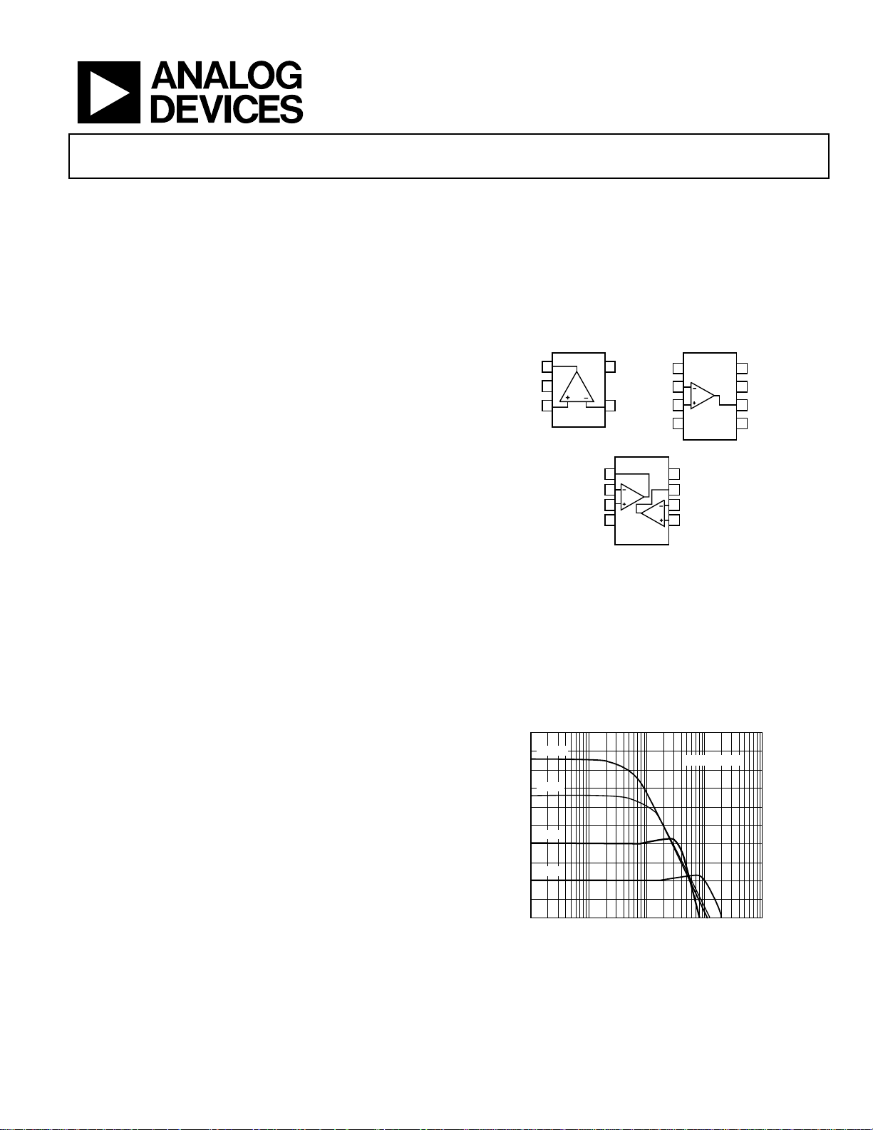
Figure 2. Small Signal Frequency Response
One Technology Way, P.O. Box 9106, Norwood, MA 02062-9106, U.S.A.
Tel: 781.329.4700 www.analog.com
Fax: 781.326.8703 © 2004 Analog Devices, Inc. All rights reserved.
V
= 200mV p-p
O
02916-E-002

AD8065/AD8066
TABLE OF CONTENTS
Specifications..................................................................................... 3
REVISION HISTORY
Absolute Maximum Ratings............................................................ 6
ESD Caution.................................................................................. 6
Maximum Power Dissipation..................................................... 7
Output Short Circuit.................................................................... 7
Typical Performance Characteristics ............................................. 8
Test Circuits..................................................................................... 15
Theory of Operation ......................................................................18
Closed-Loop Frequency Response........................................... 18
Noninverting Closed-Loop Frequency Response.................. 18
Inverting Closed-Loop Frequency Response .........................18
Wideband Operation................................................................. 19
Input Protection.......................................................................... 19
Thermal Considerations............................................................ 20
Input and Output Overload Behavior...................................... 20
Layout, Grounding, and Bypassing Considerations................... 21
Power Supply Bypassing............................................................ 21
2/04—Data Sheet Changed from Rev. D to Rev. E.
Updated Format.................................................................Universal
Updated Figure 56......................................................................... 21
Updated Outline Dimensions...................................................... 25
Updated Ordering Guide.............................................................. 26
11/03—Data Sheet changed from Rev. C to Rev. D.
Changes to Features........................................................................ 1
Changes to Connection Diagrams................................................ 1
Updated Ordering Guide................................................................ 5
Updated Outline Dimensions...................................................... 22
4/03—Data Sheet changed from Rev. B to Rev. C.
Added SOIC-8 (R) for the AD8065............................................... 4
2/03—Data Sheet changed from Rev. A to Rev. B.
Changes to Absolute Maximum Ratings...................................... 4
Changes to Test Circuit 10 ........................................................... 14
Changes to Test Circuit 11 ........................................................... 15
Changes to Noninverting Closed-Loop Frequency Response 16
Changes to Inverting Closed-Loop Frequency Response ....... 16
Updated Figure 6 .......................................................................... 18
Changes to Figure 7.......................................................................19
Changes to Figures 10................................................................... 21
Changes to Figure 11.....................................................................22
Changes to High Speed JFET Instrumentation Amplifier....... 22
Changes to Video Buffer............................................................... 22
Grounding................................................................................... 21
Leakage Currents........................................................................ 22
Input Capacitance.......................................................................22
Output Capacitance ...................................................................22
Input-to-Output Coupling........................................................ 23
Wideband Photodiode Preamp ................................................23
High Speed JFET Input Instrumentation Amplifier.............. 24
Video Buffer................................................................................ 24
Outline Dimensions....................................................................... 25
Ordering Guide........................................................................... 26
8/02—Data Sheet changed from Rev. 0 to Rev. A.
Added AD8066 ..................................................................Universal
Added SOIC-8 (R) and MSOP-8 (RM) ........................................1
Edits to General Description .........................................................1
Edits to Specifications..................................................................... 2
New Figure 2.................................................................................... 5
Changes to Ordering Guide........................................................... 5
Edits to TPCs 18, 25, and 28........................................................... 8
New TPC 36 ...................................................................................11
Added Test Circuits 10 and 11..................................................... 14
MSOP (RM-8) added....................................................................23
Rev. E | Page 2 of 28

AD8065/AD8066
SPECIFICATIONS
@ TA = 25°C, VS = ±5 V, RL = 1 kΩ, unless otherwise noted.
Table 1.
Parameter Conditions Min Typ Max Unit
DYNAMIC PERFORMANCE
−3 dB Bandwidth G = +1, VO = 0.2 V p-p (AD8065) 100 145 MHz
G = +1, VO = 0.2 V p-p (AD8066) 100 120 MHz
G = +2, VO = 0.2 V p-p 50 MHz
G = +2, VO = 2 V p-p 42 MHz
Bandwidth for 0.1 dB Flatness G = +2, VO = 0.2 V p-p 7 MHz
Input Overdrive Recovery Time G = +1, −5.5 V to +5.5 V 175 ns
Output Recovery Time G = −1, −5.5 V to +5.5 V 170 ns
Slew Rate G = +2, VO = 4 V Step 130 180 V/µs
Settling Time to 0.1% G = +2, VO = 2 V Step 55 ns
G = +2, VO = 8 V Step 205 ns
NOISE/HARMONIC PERFORMANCE
SFDR fC = 1 MHz, G = +2, VO = 2 V p-p −88 dBc
f
f
Third-Order Intercept fC = 10 MHz, RL = 100 Ω 24 dBm
Input Voltage Noise f = 10 kHz 7 nV/√Hz
Input Current Noise f = 10 kHz 0.6 fA/√Hz
Differential Gain Error NTSC, G = +2, RL = 150 Ω 0.02 %
Differential Phase Error NTSC, G = +2, RL = 150 Ω 0.02 Degree
DC PERFORMANCE
Input Offset Voltage VCM = 0 V, SOIC Package 0.4 1.5 mV
Input Offset Voltage Drift 1 17 µV/°C
Input Bias Current SOIC Package 2 6 pA
T
Input Offset Current 1 10 pA
T
Open-Loop Gain VO = ±3 V, RL = 1 kΩ 100 113 dB
INPUT CHARACTERISTICS
Common-Mode Input Impedance 1000 || 2.1 GΩ || pF
Differential Input Impedance 1000 || 4.5 GΩ || pF
Input Common-Mode Voltage Range
FET Input Range −5 to +1.7 −5.0 to +2.4 V
Usable Range See the Theory of Operation section −5.0 to +5.0 V
Common-Mode Rejection Ratio VCM = −1 V to +1 V −85 −100 dB
V
OUTPUT CHARACTERISTICS
Output Voltage Swing RL = 1 kΩ −4.88 to +4.90 −4.94 to +4.95 V
R
Output Current VO = 9 V p-p, SFDR ≥ −60 dBc, f = 500 kHz 35 mA
Short-Circuit Current 90 mA
Capacitive Load Drive 30% Overshoot G = +1 20 pF
POWER SUPPLY
Operating Range 5 24 V
Quiescent Current per Amplifier 6.4 7.2 mA
Power Supply Rejection Ratio ±PSRR −85 −100 dB
= 5 MHz, G = +2, VO = 2 V p-p −67 dBc
C
= 1 MHz, G = +2, VO = 8 V p-p −73 dBc
C
to T
MIN
MIN
CM
= 150 Ω −4.8 to +4.7 V
L
25 pA
MAX
to T
1 pA
MAX
= −1 V to +1 V (SOT-23) −82 −91 dB
Rev. E | Page 3 of 28

AD8065/AD8066
@ TA = 25°C, VS = ±12 V, RL = 1 kΩ, unless otherwise noted.
Table 2.
Parameter Conditions Min Typ Max Unit
DYNAMIC PERFORMANCE MHz
−3 dB Bandwidth G = +1, VO = 0.2 V p-p (AD8065) 100 145 MHz
G = +1, VO = 0.2 V p-p (AD8066) 100 115 MHz
G = +2, VO = 0.2 V p-p 50 MHz
G = +2, VO = 2 V p-p 40 MHz
Bandwidth for 0.1 dB Flatness G = +2, VO = 0.2 V p-p 7 MHz
Input Overdrive Recovery G = +1, −12.5 V to +12.5 V 175 ns
Output Overdrive Recovery G = −1, −12.5 V to +12.5 V 170 ns
Slew Rate G = +2, VO = 4 V Step 130 180 V/µs
Settling Time to 0.1% G = +2, VO = 2 V Step 55 ns
G = +2, VO = 10 V Step 250 ns
NOISE/HARMONIC PERFORMANCE
SFDR fC = 1 MHz, G = +2, VO = 2 V p-p −100 dBc
f
f
Third-Order Intercept fC = 10 MHz, RL = 100 Ω 24 dBm
Input Voltage Noise f = 10 kHz 7 nV/√Hz
Input Current Noise f = 10 kHz 1 fA/√Hz
Differential Gain Error NTSC, G = +2, RL = 150 Ω 0.04 %
Differential Phase Error NTSC, G = +2, RL = 150 Ω 0.03 Degree
DC PERFORMANCE
Input Offset Voltage VCM = 0 V, SOIC Package 0.4 1.5 mV
Input Offset Voltage Drift 1 17 µV/°C
Input Bias Current SOIC Package 3 7 pA
T
Input Offset Current 2 10 pA
T
Open-Loop Gain VO = ±10 V, RL = 1 kΩ 103 114 dB
INPUT CHARACTERISTICS
Common-Mode Input Impedance 1000 || 2.1 GΩ || pF
Differential Input Impedance 1000 || 4.5 GΩ || pF
Input Common-Mode Voltage Range
FET Input Range −12 to +8.5 −12.0 to +9.5 V
Usable Range See the Theory of Operation section −12.0 to +12.0 V
Common-Mode Rejection Ratio VCM = −1 V to +1 V −85 −100 dB
V
OUTPUT CHARACTERISTICS
Output Voltage Swing RL = 1 kΩ −11.8 to +11.8 −11.9 to +11.9 V
R
Output Current VO = 22 V p-p, SFDR ≥ −60 dBc, f = 500 kHz 30 mA
Short-Circuit Current 120 mA
Capacitive Load Drive 30% Overshoot G = +1 25 pF
POWER SUPPLY
Operating Range 5 24 V
Quiescent Current per Amplifier 6.6 7.4 mA
Power Supply Rejection Ratio ±PSRR −84 −93 dB
= 5 MHz, G = +2, VO = 2 V p-p −67 dBc
C
= 1 MHz, G = +2, VO = 10 V p-p −85 dBc
C
to T
MIN
MIN
CM
= 350 Ω −11.25 to +11.5 V
L
25 pA
MAX
to T
2 pA
MAX
= −1 V to +1 V (SOT-23) −82 −91 dB
Rev. E | Page 4 of 28

AD8065/AD8066
@ TA = 25°C, VS = 5 V, RL = 1 kΩ, unless otherwise noted.
Table 3.
Parameter Conditions Min Typ Max Unit
DYNAMIC PERFORMANCE
−3 dB Bandwidth G = +1, VO = 0.2 V p-p (AD8065) 125 155 MHz
G = +1, VO = 0.2 V p-p (AD8066) 110 130 MHz
G = +2, VO = 0.2 V p-p 50 MHz
G = +2, VO = 2 V p-p 43 MHz
Bandwidth for 0.1 dB Flatness G = +2, VO = 0.2 V p-p 6 MHz
Input Overdrive Recovery Time G = +1, −0.5 V to +5.5 V 175 ns
Output Recovery Time G = −1, −0.5 V to +5.5 V 170 ns
Slew Rate G = +2, VO = 2 V Step 105 160 V/µs
Settling Time to 0.1% G = +2, VO = 2 V Step 60 ns
NOISE/HARMONIC PERFORMANCE
SFDR fC = 1 MHz, G = +2, VO = 2 V p-p −65 dBc
f
Third-Order Intercept fC = 10 MHz, RL = 100 Ω 22 dBm
Input Voltage Noise f = 10 kHz 7 nV/√Hz
Input Current Noise f = 10 kHz 0.6 fA/√Hz
Differential Gain Error NTSC, G = +2, RL = 150 Ω 0.13 %
Differential Phase Error NTSC, G = +2, RL = 150 Ω 0.16 Degree
DC PERFORMANCE
Input Offset Voltage V
Input Offset Voltage Drift 1 17 µV/ºC
Input Bias Current SOIC Package 1 5 pA
T
Input Offset Current 1 5 pA
T
Open-Loop Gain VO = 1 V to 4 V (AD8065) 100 113 dB
V
INPUT CHARACTERISTICS
Common-Mode Input Impedance 1000 || 2.1 GΩ || pF
Differential Input Impedance 1000 || 4.5 GΩ || pF
Input Common-Mode Voltage Range
FET Input Range 0 to 1.7 0 to 2.4 V
Usable Range See the Theory of Operation section 0 to 5.0 V
Common-Mode Rejection Ratio VCM = 1 V to 4 V −74 −100 dB
V
OUTPUT CHARACTERISTICS
Output Voltage Swing RL = 1 kΩ 0.1 to 4.85 0.03 to 4.95 V
R
Output Current VO = 4 V p-p, SFDR ≥ −60 dBc, f = 500 kHz 35 mA
Short-Circuit Current 75 mA
Capacitive Load Drive 30% Overshoot G = +1 5 pF
POWER SUPPLY
Operating Range 5 24 V
Quiescent Current per Amplifier 5.8 6.4 7.0 mA
Power Supply Rejection Ratio ±PSRR −78 −100 dB
= 5 MHz, G = +2, VO = 2 V p-p −50 dBc
C
= 1.0 V, SOIC Package 0.4 1.5 mV
CM
to T
MIN
MIN
= 1 V to 4 V (AD8066) 90 103 dB
O
CM
= 150 Ω 0.07 to 4.83 V
L
25 pA
MAX
to T
1 pA
MAX
= 1 V to 2 V (SOT-23) −78 −91 dB
Rev. E | Page 5 of 28
AD8065/AD8066
ABSOLUTE MAXIMUM RATINGS
Table 4.
Parameter Rating
Supply Voltage 26.4 V
Power Dissipation See Figure 3
Common-Mode Input Voltage VEE − 0.5 V to VCC + 0.5 V
Differential Input Voltage 1.8 V
Storage Temperature −65°C to +125°C
Operating Temperature Range −40°C to +85°C
Lead Temperature Range
(Soldering, 10 sec)
300°C
ESD CAUTION
ESD (electrostatic discharge) sensitive device. Electrostatic charges as high as 4000 V readily accumulate on
the human body and test equipment and can discharge without detection. Although this product features
proprietary ESD protection circuitry, permanent damage may occur on devices subjected to high energy
electrostatic discharges. Therefore, proper ESD precautions are recommended to avoid performance
degradation or loss of functionality.
Stresses above those listed under Absolute Maximum Ratings
may cause permanent damage to the device. This is a stress
rating only; functional operation of the device at these or any
other conditions above those indicated in the operational
section of this specification is not implied. Exposure to absolute
maximum rating conditions for extended periods may affect
device reliability.
Rev. E | Page 6 of 28
AD8065/AD8066
(
)
(
)
MAXIMUM POWER DISSIPATION
The maximum safe power dissipation in the AD8065/AD8066
packages is limited by the associated rise in junction
temperature (T
) on the die. The plastic encapsulating the die
J
will locally reach the junction temperature. At approximately
150°C, which is the glass transition temperature, the plastic will
change its properties. Even temporarily exceeding this
temperature limit can change the stresses that the package
exerts on the die, permanently shifting the parametric
performance of the AD8065/AD8066. Exceeding a junction
temperature of 175°C for an extended period of time can result
in changes in the silicon devices, potentially causing failure.
2.0
1.5
MSOP-8
SOIC-8
1.0
SOT-23-5
0.5
MAXIMUM POWER DISSIPATION (W)
The still-air thermal properties of the package and PCB (θ
ambient temperature (T
package (P
) determine the junction temperature of the die. The
D
), and total power dissipated in the
A
JA
junction temperature can be calculated as
PTT θ×+=
J
The power dissipated in the package (
D
A
JA
P
) is the sum of the
D
quiescent power dissipation and the power dissipated in the
package due to the load drive for all outputs. The quiescent
V
power is the voltage between the supply pins (
quiescent current (I
midsupply, then the total drive power is
). Assuming the load (RL) is referenced to
S
VS /2 × I
) times the
S
, some of
OUT
which is dissipated in the package and some in the load (V
I
). The difference between the total drive power and the load
OUT
power is the drive power dissipated in the package.
PowerLoadPowerDriveTotalPowerQuiescentP
D
⎛
()
D
IVP
S
⎜
SS
2
⎝
VV
×+×=
OUT
R
V
OUT
⎞
−
⎟
R
L
L
⎠
RMS output voltages should be considered. If
V
−, as in single-supply operation, then the total drive power is
S
V
× I
.
S
OUT
−+=
2
R
is referenced to
L
OUT
),
0
AMBIENT TEMPERATURE (°C)
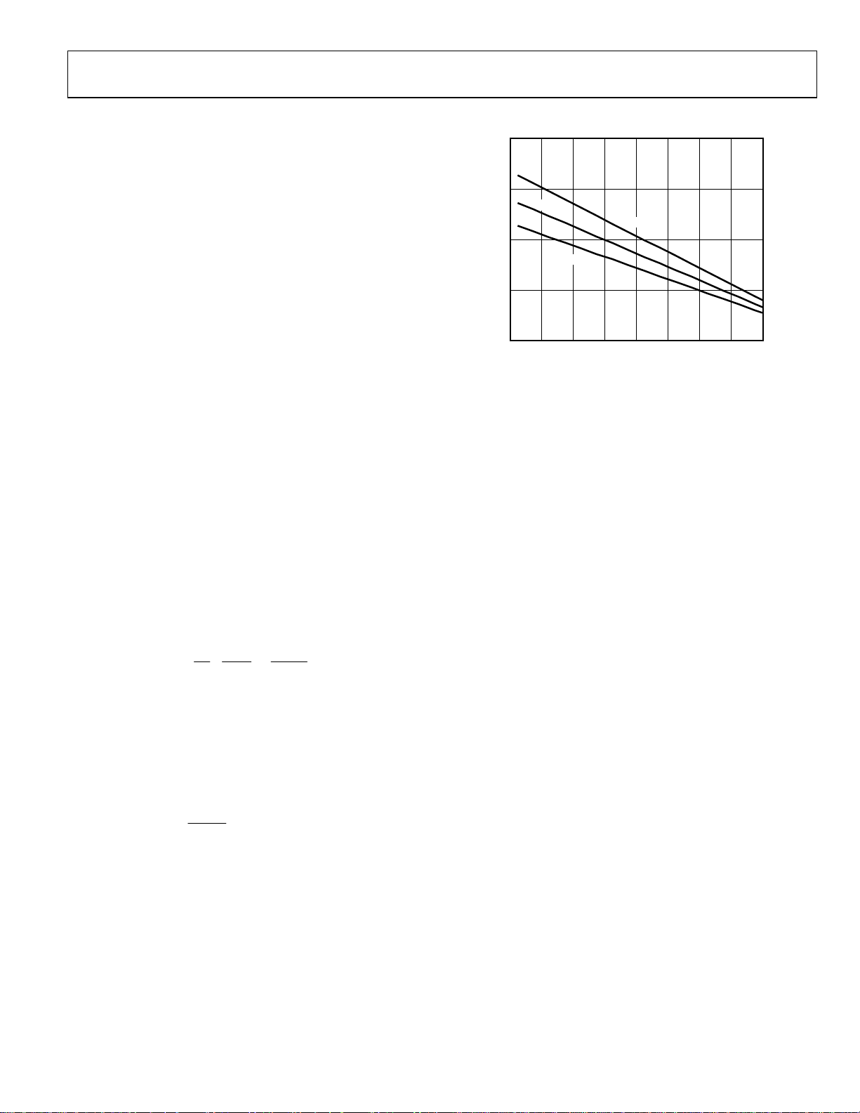
Figure 3. Maximum Power Dissipation vs. Temperature for a 4-Layer Board
200–40 –20–60 40 60 80 100
02916-E-003
Airflow will increase heat dissipation, effectively reducing θJA.
Also, more metal directly in contact with the package leads
from metal traces, through holes, ground, and power planes will
reduce the θ
. Care must be taken to minimize parasitic
JA
capacitances at the input leads of high speed op amps as
discussed in the Layout, Grounding, and Bypassing
Considerations section.
Figure 3 shows the maximum safe power dissipation in the
×
package versus the ambient temperature for the SOIC
(125°C/W), SOT-23 (180°C/W), and MSOP (150°C/W)
packages on a JEDEC standard 4-layer board. θ
values are
JA
approximations.
OUTPUT SHORT CIRCUIT
Shorting the output to ground or drawing excessive current for
the AD8065/AD8066 will likely cause catastrophic failure.
If the rms signal levels are indeterminate, then consider the
V
worst case, when
()
D
In single-supply operation with R
is V
= VS/2.
OUT
= VS/4 for RL to midsupply.
OUT
2
()
4/
V
S
+×=
IVP
SS
R
L
referenced to VS−, worst case
L
Rev. E | Page 7 of 28
AD8065/AD8066
TYPICAL PERFORMANCE CHARACTERISTICS
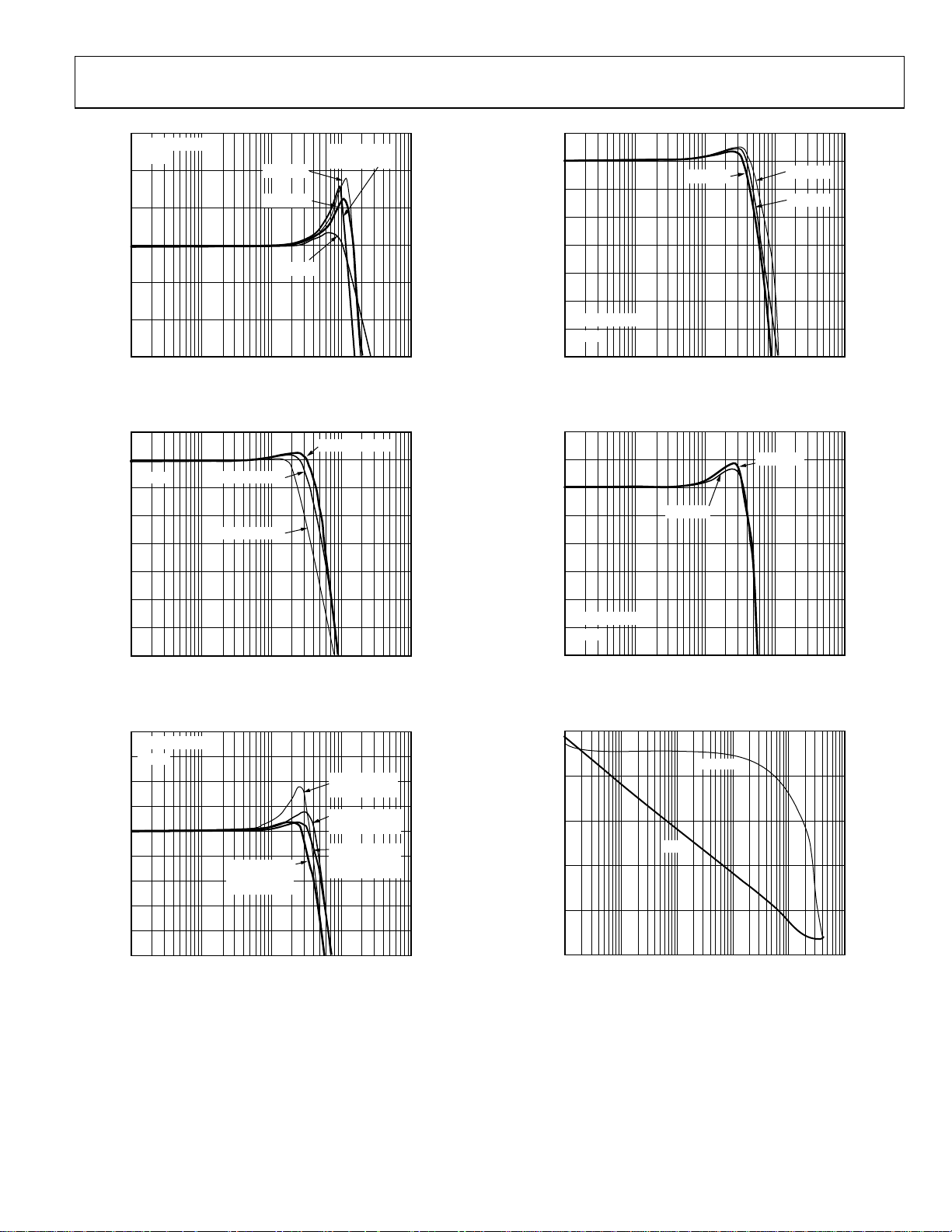
Default Conditions: ±5 V, CL = 5 pF, RL = 1 kΩ, V
24
21
G = +10
18
G = +5
15
12
9
G = +2
GAIN (dB)
6
3
G = +1
0
–3
–6
10.1 10 100 1000
FREQUENCY (MHz)
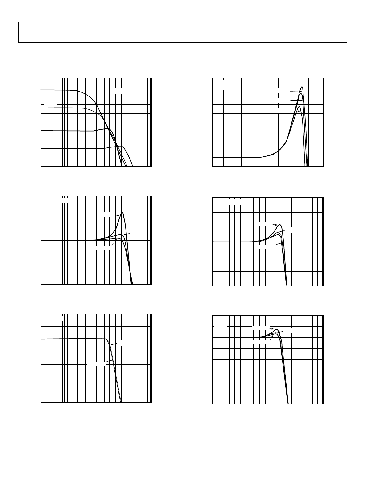
Figure 4. Small Signal Frequency Response for Various Gains
6
VO = 200mV p-p
G = +1
4
2
0
GAIN (dB)
–2
V
S
V
S
= ±12V
= +5V
= 200mV p-p
V
O
= 2 V p-p, Temperature = 25°C.
OUT
02916-E-004
V
= ±5V
S
6.9
RL = 150Ω
6.8
G = +2
6.7
6.6
6.5
6.4
GAIN (dB)
6.3
6.2
6.1
6.0
5.9
0.1 101 100
V
= 0.2V p-p
OUT
V
= 0.7V p-p
OUT
V
= 1.4V p-p
OUT
FREQUENCY (MHz)
Figure 7. 0.1 dB Flatness Frequency Response (See Figure 43)
9
VO = 200mV p-p
G = +2
8
7
6
GAIN (dB)
5
VS = +5V
V
= ±12V
S
V
= ±5V
S
02916-E-007
–4
–6
10.1 10 100 1000
FREQUENCY (MHz)
Figure 5. Small Signal Frequency Response for Various Supplies (See Figure 42)
2
VO = 2V p-p
G = +1
1
0
–1
V
–2
GAIN (dB)
–3
–4
–5
10.1 10 100 1000
= ±12V
S
FREQUENCY (MHz)
V
= ±5V
S
Figure 6. Large Signal Frequency Response for Various Supplies (See Figure 42)
4
3
02916-E-005
10.1 10 100 1000
FREQUENCY (MHz)
02916-E-008
Figure 8. Small Signal Frequency Response for Various Supplies (See Figure 43)
8
G = +2
7
6
5
4
GAIN (dB)
3
2
1
0
02916-E-006
VS = +5V
V
= ±12V
S
10.1 10 100 1000
FREQUENCY (MHz)
V
= ±5V
S
02916-E-009
Figure 9. Large Signal Frequency Response for Various Supplies (See Figure 43)
Rev. E | Page 8 of 28
AD8065/AD8066
9
VO = 200mV p-p
G = +1
6
3
C
= 25pF
L
CL = 20pF
C
R
= 25pF
L
SNUB
= 20
Ω
8
6
4
2
C
= 5pF
L
= 55pF
C
L
CL = 25pF
0
GAIN (dB)
–3
–6
–9
10.1 10 100 1000
FREQUENCY (MHz)
Figure 10. Small Signal Frequency Response for Various C
8
6
G = +2
4
2
0
GAIN (dB)
–2
–4
–6
–8
V
OUT
V
OUT
10.1 10 100 1000
FREQUENCY (MHz)
= 2V p-p
= 4V p-p
C
= 5pF
L
V
OUT
LOAD
= 0.2V p-p
(See Figure 42)
Figure 11. Frequency Response for Various Output Amplitudes (See Figure 43)
14
VO = 200mV p-p
12
G = +2
R
10
8
6
4
GAIN (dB)
2
0
–2
–4
R
= RG = 1kΩ,
F
= 500Ω,
R
S
= 3.3pF
C
F
10.1 10 100 1000
FREQUENCY (MHz)
Figure 12. Small Signal Frequency Response for Various R
= RG = 1kΩ,
F
= 500
Ω
R
S
RF = RG = 500Ω,
R
= 250
Ω
S
RF = RG = 500Ω,
= 250Ω,
R
S
C
= 2.2pF
F
(See Figure 43)
F/CF
0
GAIN (dB)
–2
–4
VO = 200mV p-p
–6
G = +2
–8
02916-E-010
Figure 13. Small Signal Frequency Response for Various C
8
7
6
5
4
GAIN (dB)
3
2
VO = 200mV p-p
1
G = +2
0
02916-E-011
Figure 14. Small Signal Frequency Response for Various R
80
60
40
20
OPEN-LOOP GAIN (dB)
0
–20
0.01 0.1 1 10 100 1000
02916-E-012
10.1 10 100 1000
FREQUENCY (MHz)
(See Figure 43)
LOAD
RL = 100
Ω
RL = 1k
Ω
10.1 10 100 1000
FREQUENCY (MHz)
(See Figure 43)
LOAD
PHASE
GAIN
FREQUENCY (MHz)
120
60
0
–60
–120
–180
02916-E-013
02916-E-014
PHASE (DEGREES)
02916-E-015
Figure 15. Open-Loop Response
Rev. E | Page 9 of 28
 Loading...