

Analog Devices AD8063, AD8062, AD8061 Datasheet
Low-Cost, 300 MHz
8
7
6
5
1
2
3
4
NC
–IN
+IN
DISABLE
(AD8063 ONLY)
+V
S
V
OUT
NC–V
S
AD8061/
AD8063
NC = NO CONNECT
(Not to Scale)
a
FEATURES
Low Cost
Single (AD8061), Dual (AD8062)
Single with Disable (AD8063)
Rail-to-Rail Output Swing
6 mV V
High Speed
300 MHz, –3 dB Bandwidth (G = 1)
800 V/s Slew Rate
8.5 nV/√Hz @ 5 V
35 ns Settling Time to 0.1% with 1 V Step
Operates on 2.7 V to 8 V Supplies
Input Voltage Range = –0.2 V to +3.2 V with V
Excellent Video Specs (R
Gain Flatness 0.1 dB to 30 MHz
0.01% Differential Gain Error
0.04ⴗ Differential Phase Error
35 ns Overload Recovery
Low Power
6.8 mA/Amplifier Typical Supply Current
AD8063 400 A when Disabled
Small Packaging
AD8061 Available in SOIC-8 and SOT-23-5
AD8062 Available in SOIC-8 and SOIC
AD8063 Available in SOIC-8 and SOT-23-6
APPLICATIONS
Imaging
Photodiode Preamp
Professional Video and Cameras
Hand Sets
DVD/CD
Base Stations
Filters
A-to-D Driver
PRODUCT DESCRIPTION
The AD8061, AD8062, and AD8063 are rail-to-rail output voltage feedback amplifiers offering ease of use and low cost. They
have bandwidth and slew rate typically found in current feedback amplifiers. All have a wide input common-mode voltage
range and output voltage swing, making them easy to use on
single supplies as low as 2.7 V.
Despite being low cost, the AD8061, AD8062, and AD8063
provide excellent overall performance. For video applications
their differential gain and phase errors are 0.01% and 0.04°
into a 150 Ω load, along with 0.1 dB flatness out to 30 MHz.
Additionally, they offer wide bandwidth to 300 MHz along
with 800 V/µs slew rate.
OS
= 150 ⍀, G = 2)
L
= 5
S
Rail-to-Rail Amplifiers
AD8061/AD8062/AD8063
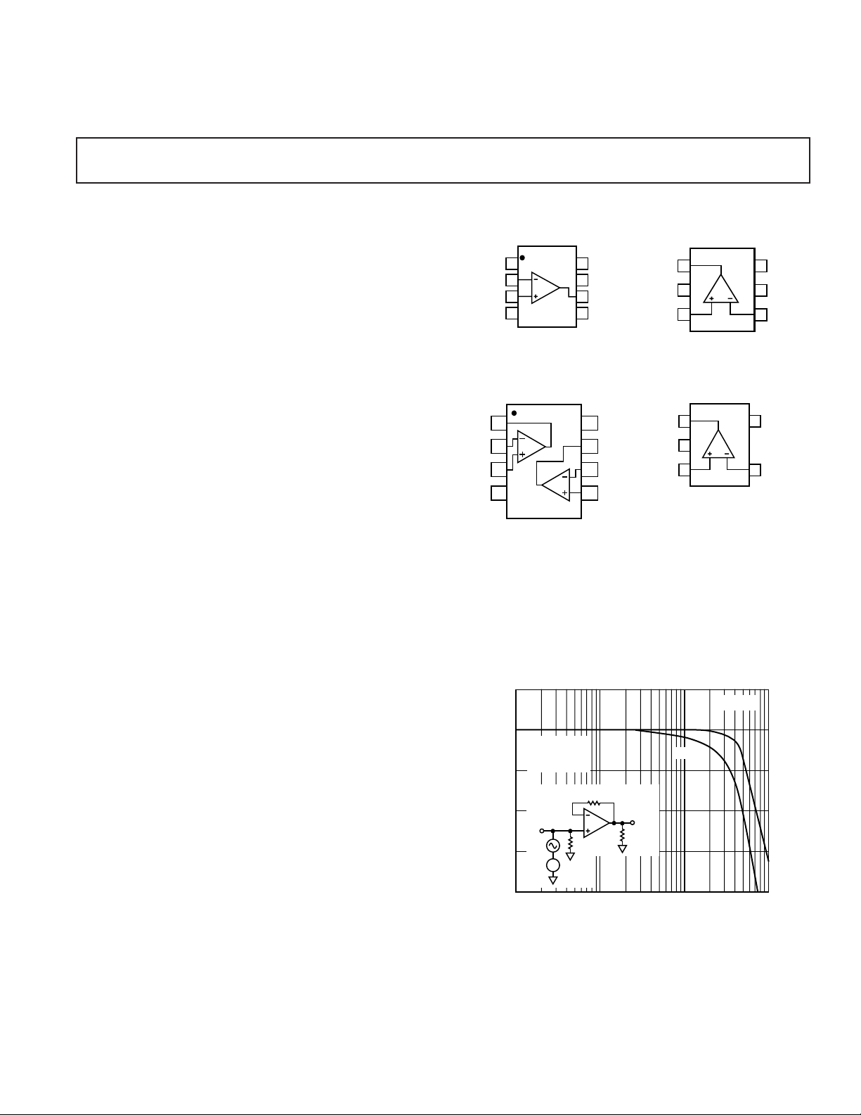
CONNECTION DIAGRAMS
(Top Views)
SOIC-8 (R) SOT-23-6 (RT)
AD8063
1
2
S
3
(Not to Scale)
SOT-23-5 (RT)
AD8061
1
2
S
3
(Not to Scale)
SOIC-8 (R) and SOIC (RM)
1
2
3
4
(Not to Scale)
AD8062
+V
8
S
V
7
OUT2
–IN2
6
+IN2
5
V
OUT1
–IN1
+IN1
–V
S
V
OUT
–V
+IN
V
OUT
–V
+IN
The AD8061, AD8062, and AD8063 offer a typical low power
of 6.8 mA/amplifier, while being capable of delivering up to
50 mA of load current. The AD8063 has a power-down disable
feature that reduces the supply current to 400 µA. These features
make the AD8063 ideal for portable and battery-powered
applications where size and power is critical.
3
0
VO = 0.2V p-p
= 1kV
R
L
= 1V
V
BIAS
–3
–6
IN
NORMALIZED GAIN – dB
–9
–12
1
50V
6
V
BIAS
R
F
OUT
R
L
FREQUENCY – MHz
RF = 0V
RF = 50V
10010
Figure 1. Small Signal Response, RF = 0 Ω, 50
6
5
4
5
4
1000
+V
S
DISABLE
–IN
+V
S
–IN
Ω
REV. A
Information furnished by Analog Devices is believed to be accurate and
reliable. However, no responsibility is assumed by Analog Devices for its
use, nor for any infringements of patents or other rights of third parties
which may result from its use. No license is granted by implication or
otherwise under any patent or patent rights of Analog Devices.
One Technology Way, P.O. Box 9106, Norwood, MA 02062-9106, U.S.A.
Tel: 781/329-4700 World Wide Web Site: http://www.analog.com
Fax: 781/326-8703 © Analog Devices, Inc., 2000

(TA = 25ⴗC, VS = 5 V, RL = 1 k⍀, VO = 1 V,
AD8061/AD8062/AD8063–SPECIFICATIONS
Parameter Conditions Min Typ Max Unit
DYNAMIC PERFORMANCE
–3 dB Small Signal Bandwidth G = 1, VO = 0.2 V p-p 150 320 MHz
G = –1, +2, V
–3 dB Large Signal Bandwidth G = 1, V
Bandwidth for 0.1 dB Flatness G = 1, V
Slew Rate G = 1, V
G = 2, V
Settling Time to 0.1% G = 2, VO = 2 V Step 35 ns
NOISE/DISTORTION PERFORMANCE
Total Harmonic Distortion fC = 5 MHz, VO = 2 V p-p, R
f
= 20 MHz, VO = 2 V p-p, R
C
Crosstalk, Output to Output f = 5 MHz, G = 2, AD8062 –90 dBc
Input Voltage Noise f = 100 kHz 8.5 nV/√Hz
Input Current Noise f = 100 kHz 1.2 pA/√Hz
Differential Gain Error (NTSC) G = 2, R
Differential Phase Error (NTSC) G = 2, R
Third Order Intercept f = 10 MHz 28 dBc
SFDR f = 5 MHz 62 dB
DC PERFORMANCE
Input Offset Voltage 16mV
to T
T
MIN
Input Offset Voltage Drift 3.5 µV/°C
Input Bias Current 3.5 9 µA
to T
T
MIN
Input Offset Current 0.3 4.5 ±µA
Open-Loop Gain VO = 0.5 V to 4.5 V, R
VO = 0.5 V to 4.5 V, R
INPUT CHARACTERISTICS
Input Resistance 13 MΩ
Input Capacitance 1pF
Input Common-Mode Voltage Range –0.2 to +3.2 V
Common-Mode Rejection Ratio VCM = –0.2 V to +3.2 V 62 80 dB
OUTPUT CHARACTERISTICS
Output Voltage Swing—Load Resistance R
Is Terminated at Midsupply R
Output Current V
Capacitive Load Drive, V
= 0.8 V 30% Overshoot: G = 1, R
OUT
= 150 Ω 0.3 0.1 to 4.5 4.75 V
L
= 2␣ kΩ 0.25 0.1 to 4.9 4.85 V
L
= 0.5 V to 4.5 V 25 50 mA
O
G = 2, R
POWER-DOWN DISABLE
Turn-On Time 40 ns
Turn-Off Time 300 ns
DISABLE Voltage—Off 2.8 V
DISABLE Voltage—On 3.2 V
POWER SUPPLY
Operating Range 2.7 5 8 V
Quiescent Current per Amplifier 6.8 9.5 mA
Supply Current when Disabled 0.4 mA
(AD8063 Only)
Power Supply Rejection Ratio ∆V
Specifications subject to change without notice.
= 2.7 V to 5 V 72 80 dB
S
= 0.2 V p-p 60 115 MHz
O
= 1 V p-p 280 MHz
O
= 0.2 V p-p 30 MHz
O
= 2 V Step, R
O
= 2 V Step, R
O
= 150 Ω 0.01 %
L
= 150 Ω 0.04 Degree
L
MAX
MAX
= 2 kΩ 500 650 V/µs
L
= 2 kΩ 300 500 V/µs
L
= 1 kΩ –77 dBc
L
= 1 kΩ –50 dBc
L
= 150 Ω 68 70 dB
L
= 2 kΩ 74 90 dB
L
= 0 Ω 25 pF
S
= 4.7 Ω 300 pF
S
unless otherwise noted)
26mV
49µA
–2–
REV. A

AD8061/AD8062/AD8063
SPECIFICATIONS
Parameter Conditions Min Typ Max Unit
DYNAMIC PERFORMANCE
–3 dB Small Signal Bandwidth G = 1, VO = 0.2 V p-p 150 300 MHz
–3 dB Large Signal Bandwidth G = 1, V
Bandwidth for 0.1 dB Flatness G = 1, V
Slew Rate G = 1, V
Settling Time to 0.1% G = 2, VO = 1 V Step 40 ns
NOISE/DISTORTION PERFORMANCE
Total Harmonic Distortion f
Crosstalk, Output to Output f = 5 MHz, G = 2 –90 dBc
Input Voltage Noise f = 100 kHz 8.5 nV/√Hz
Input Current Noise f = 100 kHz 1.2 pA/√Hz
DC PERFORMANCE
Input Offset Voltage 16mV
Input Offset Voltage Drift 3.5 µV/°C
Input Bias Current 3.5 8.5 µA
Input Offset Current 0.3 4.5 ±µA
Open-Loop Gain VO = 0.5 V to 2.5 V, R
INPUT CHARACTERISTICS
Input Resistance 13 MΩ
Input Capacitance 1pF
Input Common-Mode Voltage Range –0.2 to +1.2 V
Common-Mode Rejection Ratio VCM = –0.2 V to +1.2 V 80 dB
OUTPUT CHARACTERISTICS
Output Voltage Swing R
Output Current V
Capacitive Load Drive, V
POWER-DOWN DISABLE
Turn-On Time 40 ns
Turn-Off Time 300 ns
DISABLE Voltage—Off 0.8 V
DISABLE Voltage—On 1.2 V
POWER SUPPLY
Operating Range 2.7 3 V
Quiescent Current per Amplifier 6.8 9 mA
Supply Current when Disabled 0.4 mA
(AD8063 Only)
Power Supply Rejection Ratio 72 80 dB
OUT
(TA = 25ⴗC, VS = 3 V, RL = 1 k⍀, VO = 1 V, unless otherwise noted)
G = –1, +2, V
G = 2, V
= 5 MHz, VO = 2 V p-p, R
C
= 20 MHz, VO = 2 V p-p, R
f
C
to T
T
MIN
to T
T
MIN
VO = 0.5 V to 2.5 V, R
= 150 Ω 0.3 0.1 to 2.87 2.85 V
L
= 2␣ kΩ 0.3 0.1 to 2.9 2.90 V
R
L
= 0.5 V to 2.5 V 25 mA
O
= 0.8 V 30% Overshoot, G = 1, R
G = 2, R
= 0.2 V p-p 60 115 MHz
O
= 1 V p-p 250 MHz
O
= 0.2 V p-p 30 MHz
O
= 1 V Step, R
O
= 1.5 V Step, R
O
MAX
MAX
= 2 kΩ 190 280 V/µs
L
= 2 kΩ 180 230 V/µs
L
= 1 kΩ –60 dBc
L
= 1 kΩ –44 dBc
L
= 150 Ω 66 70 dB
L
= 2 kΩ 74 90 dB
L
= 0 Ω,25 pF
S
= 4.7 Ω 300 pF
S
26mV
4 8.5 µA
Specifications subject to change without notice.
REV. A
–3–

(TA = 25ⴗC, VS = 2.7 V, RL = 1 k⍀, VO = 1 V,
AD8061/AD8062/AD8063–SPECIFICATIONS
Parameter Conditions Min Typ Max Unit
DYNAMIC PERFORMANCE
–3 dB Small Signal Bandwidth G = 1, VO = 0.2 V p-p 150 300 MHz
G = –1, +2, V
G = 1, V
Bandwidth for 0.1 dB Flatness G = 1, V
Slew Rate G = 1, V
G = 2, V
Settling Time to 0.1% G = 2, VO = 1 V Step 40 ns
NOISE/DISTORTION PERFORMANCE
Total Harmonic Distortion fC = 5 MHz, VO = 2 V p-p, R
f
= 20 MHz, VO = 2 V p-p, R
C
Crosstalk, Output to Output f = 5 MHz, G = 2 –90 dBc
Input Voltage Noise f = 100 kHz 8.5 nV/√Hz
Input Current Noise f = 100 kHz 1.2 pA/√Hz
DC PERFORMANCE
Input Offset Voltage 16mV
to T
T
MIN
Input Offset Voltage Drift 3.5 µV/°C
Input Bias Current 3.5 µA
to T
T
MIN
Input Offset Current 0.3 4.5 ±µA
Open-Loop Gain VO = 0.5 V to 2.2 V, R
VO = 0.5 V to 2.2 V, R
INPUT CHARACTERISTICS
Input Resistance 13 MΩ
Input Capacitance 1pF
Input Common-Mode Voltage Range –0.2 to +0.9 V
Common-Mode Rejection Ratio VCM = –0.2 V to +0.9 V 80 dB
OUTPUT CHARACTERISTICS
Output Voltage Swing R
Output Current V
Capacitive Load Drive, V
= 0.8 V 30% Overshoot: G = 1, R
OUT
= 150 Ω 0.3 0.1 to 2.55 2.55 V
L
R
= 2␣ kΩ 0.25 0.1 to 2.6 2.6 V
L
= 0.5 V to 2.2 V 25 mA
O
G = 2, R
POWER-DOWN DISABLE
Turn-On Time 40 ns
Turn-Off Time 300 ns
DISABLE Voltage—Off 0.5 V
DISABLE Voltage—On 0.9 V
POWER SUPPLY
Operating Range 2.7 8 V
Quiescent Current per Amplifier 6.8 8.5 mA
Supply Current when Disabled 0.4 mA
(AD8063 Only)
Power Supply Rejection Ratio 80 dB
= 0.2 V p-p 60 115 MHz
O
= 1 V p-p 230 MHz
O
= 0.2 V p-p, VO DC = 1 V 30 MHz
O
= 0.7 V Step, R
O
= 1.5 V Step, R
O
MAX
MAX
= 2 kΩ 110 150 V/µs
L
= 2 kΩ 95 130 V/µs
L
= 1 kΩ –60 dBc
L
= 1 kΩ –44 dBc
L
= 150 Ω 63 70 dB
L
= 2 kΩ 74 90 dB
L
= 0␣ Ω,25 pF
S
= 4.7␣ Ω 300 pF
S
unless otherwise noted)
26mV
48.5µA
Specifications subject to change without notice.
–4–
REV. A
AD8061/AD8062/AD8063
ABSOLUTE MAXIMUM RATINGS
Supply Voltage . . . . . . . . . . . . . . . . . . . . . . . . . . . . . . . . . . 8 V
Internal Power Dissipation
2
1
Plastic Package (N) . . . . . . . . . . . . . . . . . . . . . . . . . . . . 1.3 W
Small Outline Package (R) . . . . . . . . . . . . . . . . . . . . . . . 0.8 W
SOT-23-5 Package . . . . . . . . . . . . . . . . . . . . . . . . . . . . 0.5 W
SOT-23-6 Package . . . . . . . . . . . . . . . . . . . . . . . . . . . . 0.5 W
µSOIC Package . . . . . . . . . . . . . . . . . . . . . . . . . . . . . . . 0.6 W
Input Voltage (Common-Mode) (–V
Differential Input Voltage . . . . . . . . . . . . . . . . . . . . . . . . ±V
– 0.2 V) to (+VS – 1.8 V)
S
S
Output Short Circuit Duration
. . . . . . . . . . . . . . . . . . . . . . Observe Power Derating Curves
Storage Temperature Range R, RM, SOT-23-5,
SOT-23-6 . . . . . . . . . . . . . . . . . . . . . . . . –65°C to +125°C
Operating Temperature Range . . . . . . . . . . . –40°C to +85°C
Lead Temperature Range (Soldering 10 sec) . . . . . . . . 300°C
NOTES
1
Stresses above those listed under Absolute Maximum Ratings may cause perma-
nent damage to the device. This is a stress rating only; functional operation of the
device at these or any other conditions above those indicated in the operational
section of this specification is not implied. Exposure to absolute maximum rating
conditions for extended periods may affect device reliability.
2
Specification is for device in free air:
8-Lead SOIC Package: θJA = 160°C/W; θJC = 56°C/W
5-Lead SOT-23-5 Package: θJA = 240°C/W; θJC = 92°C/W
6-Lead SOT-23-6 Package: θJA = 230°C/W; θJC = 92°C/W
8-Lead µSOIC Package: θJA = 200°C/W; θJC = 44°C/W.
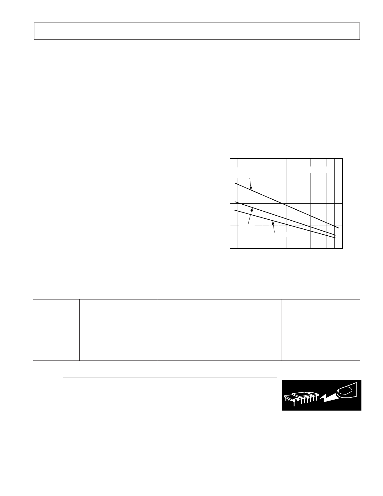
MAXIMUM POWER DISSIPATION
The maximum power that can be safely dissipated by the AD806x
is limited by the associated rise in junction temperature. The
maximum safe junction temperature for plastic encapsulated
devices is determined by the glass transition temperature of the
plastic, approximately 150°C. Temporarily exceeding this limit
may cause a shift in parametric performance due to a change
in the stresses exerted on the die by the package. Exceeding a
junction temperature of 175°C for an extended period can result
in device failure. While the AD806x is internally short circuit
protected, this may not be sufficient to guarantee that the
maximum junction temperature (150°C) is not exceeded under
all conditions.
To ensure proper operation, it is necessary to observe the
maximum power derating curves.
2.0
8-LEAD SOIC
PACKAGE
1.5
1.0
0.5
mSOIC
MAXIMUM POWER DISSIPATION – Watts
0
–30
–50 –40
SOT-23-5, -6
AMBIENT TEMPERATURE – 8C
2010
TJ = 1508C
605040300–10–20
70 80
90
Figure 2. Plot of Maximum Power Dissipation vs.
Temperature for AD8061/AD8062/AD8063
ORDERING GUIDE
Model Temperature Range Package Description Package Option
AD8061AR –40°C to +85°C 8-Lead SOIC R-8
AD8061ART –40°C to +85°C 5-Lead SOT-23-5 RT-5
AD8062AR –40°C to +85°C 8-Lead SOIC R-8
AD8062ARM –40°C to +85°C 8-Lead µSOIC RM-8
AD8063AR –40°C to +85°C 8-Lead SOIC R-8
AD8063ART –40°C to +85°C 6-Lead SOT-23-6 RT-6
AD806x-EB Evaluation Board for AD806xAR
CAUTION
ESD (electrostatic discharge) sensitive device. Electrostatic charges as high as 4000 V readily
accumulate on the human body and test equipment and can discharge without detection. Although
WARNING!
the AD8061/AD8062/AD8063 features proprietary ESD protection circuitry, permanent damage
may occur on devices subjected to high energy electrostatic discharges. Therefore, proper ESD
precautions are recommended to avoid performance degradation or loss of functionality.
ESD SENSITIVE DEVICE
REV. A
–5–
 Loading...