Analog Devices AD8057 8 b Datasheet

Low Cost, High Performance
Voltage Feedback, 325 MHz Amplifiers
AD8057/AD8058
FEATURES
Low Cost Single (AD8057) and Dual (AD8058)
High Speed
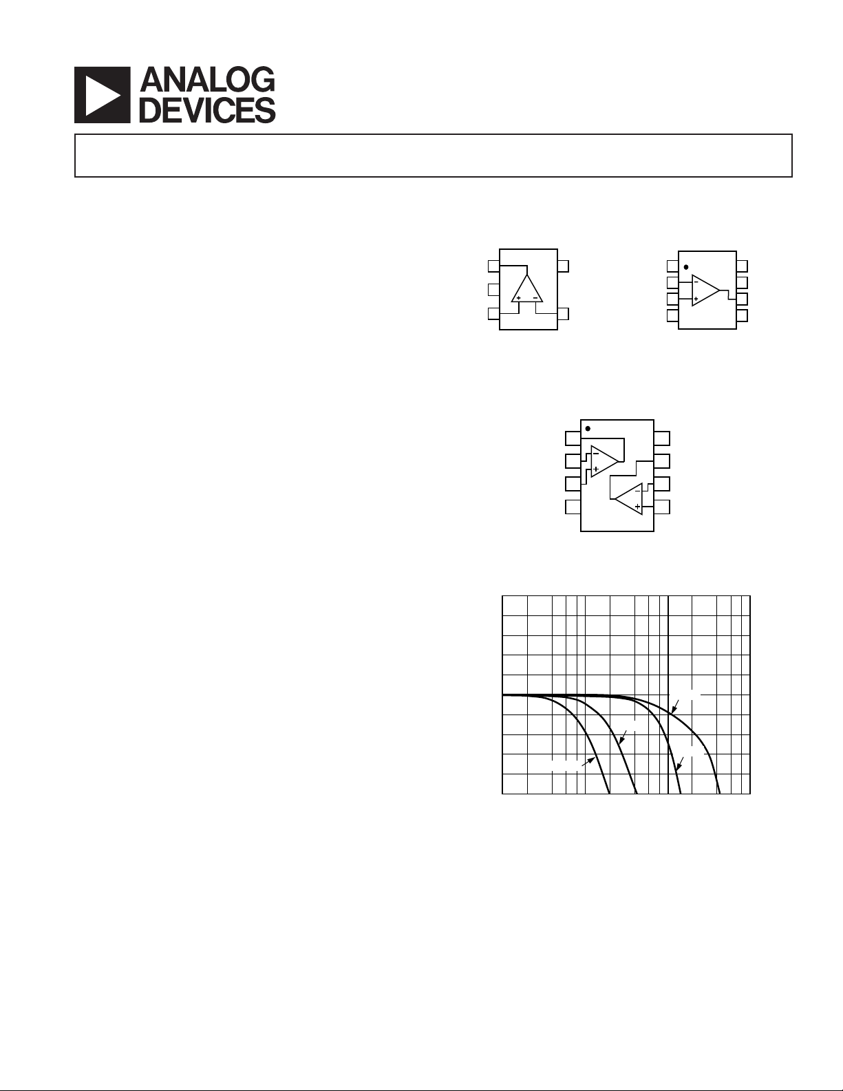
325 MHz –3 dB Bandwidth (G = +1)
1000 V/s Slew Rate
Gain Flatness 0.1 dB to 28 MHz
Low Noise
7 nV/√Hz
Low Power
5.4 mA/Amplifier Typical Supply Current @ 5 V
Low Distortion
–85 dBc @ 5 MHz, R
= 1 k⍀
L
Wide Supply Range from 3 V to 12 V
Small Packaging
AD8057 Available in SOIC-8 and SOT-23-5
AD8058 Available in SOIC-8 and MSOP
APPLICATIONS
Imaging
DVD/CD
Photodiode Preamp
A-to-D Driver
Professional Cameras
Filters
GENERAL DESCRIPTION
The AD8057 (single) and AD8058 (dual) are very high performance amplifiers with a very low cost. The balance between
cost and performance make them ideal for many applications.
The AD8057 and AD8058 will reduce the need to qualify a
variety of specialty amplifiers.
The AD8057 and AD8058 are voltage feedback amplifiers with
the bandwidth and slew rate normally found in current feedback
amplifiers. The AD8057 and AD8058 are low power amplifiers
having low quiescent current and a wide supply range from 3 V
to 12 V. They have noise and distortion performance required
for high end video systems as well as dc performance parameters
rarely found in high speed amplifiers.
The AD8057 and AD8058 are available in standard SOIC
packaging as well as tiny SOT-23-5 (AD8057) and MSOP
(AD8058) packages. These amplifiers are available in the industrial temperature range of –40°C to +85°C.
CONNECTION DIAGRAMS (TOP VIEW)
RT-5 (SOT-23-5)
1
2
S
3
(Not to Scale)
AD8057
V
OUT
–V
+IN
+V
5
S
4
–IN
R-8 (SOIC)
1
NC
2
–IN
3
+IN
AD8057
4
S
(Not to Scale)
NC = NO CONNECT
RM-8 (MSOP)
R-8 (SOIC)
OUT1
–IN1
+IN1
–V
5
4
3
2
1
0
GAIN (dB)
–1
–2
–3
–4
–5
1 100010
S
G = +10
AD8058
1
2
3
4
(Not to Scale)
G = +5
FREQUENCY (MHz)
8
7
5
6
100
+V
S
OUT2
–IN2
+IN2
G = +1
G = +2
Figure 1. Small Signal Frequency Response
8
NC
7
+V
S
6
V
OUT
5
NC–V
REV. B
Information furnished by Analog Devices is believed to be accurate and
reliable. However, no responsibility is assumed by Analog Devices for its
use, nor for any infringements of patents or other rights of third parties that
may result from its use. No license is granted by implication or otherwise
under any patent or patent rights of Analog Devices. Trademarks and
registered trademarks are the property of their respective owners.
One Technology Way, P.O. Box 9106, Norwood, MA 02062-9106, U.S.A.
Tel: 781/329-4700 www.analog.com
Fax: 781/326-8703 © 2003 Analog Devices, Inc. All rights reserved.

(@ TA = 25ⴗC, VS = ⴞ5 V, RL = 100 ⍀, RF = 0 ⍀, Gain = +1,
AD8057/AD8058–SPECIFICATIONS
unless otherwise noted.)
AD8057/AD8058
Parameter Conditions Min Typ Max Unit
DYNAMIC PERFORMANCE
–3 dB Bandwidth G = +1, VO = 0.2 V p-p 325 MHz
G = –1, V
G = +1, V
Bandwidth for 0.1 dB Flatness G = +1, V
= 0.2 V p-p 95 MHz
O
= 2 V p-p 175 MHz
O
= 0.2 V p-p 30 MHz
O
Slew Rate G = +1, VO = 2 V Step, RL = 2 kΩ 850 V/µs
G = +1, V
= 4 V Step, RL = 2 kΩ 1150 V/µs
O
Settling Time to 0.1% G = +2, VO = 2 V Step 30 ns
NOISE/HARMONIC PERFORMANCE
Total Harmonic Distortion f
SFDR f = 5 MHz, V
Third Order Intercept f = 5 MHz, V
= 5 MHz, VO = 2 V p-p, RL = 1 kΩ –85 dBc
C
f
= 20 MHz, VO = 2 V p-p, RL = 1 kΩ –62 dBc
C
= 2 V p-p, RL = 150 Ω –68 dB
O
= 2 V p-p –35 dBm
O
Crosstalk, Output to Output f = 5 MHz, G = +2 –60 dB
Input Voltage Noise f = 100 kHz 7 nV/√Hz
Input Current Noise f = 100 kHz 0.7 pA/√Hz
Differential Gain Error NTSC, G = +2, RL = 150 Ω 0.01 %
NTSC, G = +2, R
Differential Phase Error NTSC, G = +2, R
NTSC, G = +2, R
= 1 kΩ 0.02 %
L
= 150 Ω 0.15 Degree
L
= 1 kΩ 0.01 Degree
L
Overload Recovery VIN = 200 mV p-p, G = +1 30 ns
DC PERFORMANCE
Input Offset Voltage 15mV
T
MIN
to T
MAX
2.5 mV
Input Offset Voltage Drift 3 µV/°C
Input Bias Current 0.5 2.5 µA
T
MIN
to T
MAX
3.0 µA
Input Offset Current ±0.75 µA
Open-Loop Gain V
= ±2.5 V, RL = 2 kΩ 50 55 dB
O
VO = ±2.5 V, RL = 150 Ω 50 52 dB
INPUT CHARACTERISTICS
Input Resistance 10 MΩ
Input Capacitance +Input 2 pF
Input Common-Mode Voltage Range R
= 1 kΩ –4.0 +4.0 V
L
Common-Mode Rejection Ratio VCM = ±2.5 V 48 60 dB
OUTPUT CHARACTERISTICS
Output Voltage Swing RL = 2 kΩ –4.0 +4.0 V
= 150 Ω±3.9 V
R
L
Capacitive Load Drive 30% Overshoot 30 pF
POWER SUPPLY
Operating Range ±5.0 V
Quiescent Current for AD8057 6.0 7.5 mA
Quiescent Current for AD8058 14.0 15 mA
Power Supply Rejection Ratio VS = ±5 V to ± 1.5 V 54 59 dB
Specifications subject to change without notice.
REV. B–2–

AD8057/AD8058
SPECIFICATIONS
(@ TA = 25ⴗC, VS = 5 V, RL = 100 ⍀, RF = 0 ⍀, Gain = +1, unless otherwise noted.)
AD8057/AD8058
Parameter Conditions Min Typ Max Unit
DYNAMIC PERFORMANCE
–3 dB Bandwidth G = +1, V
= 0.2 V p-p 300 MHz
O
G = +1, VO = 2 V p-p 155 MHz
Bandwidth for 0.1 dB Flatness V
Slew Rate G = +1, V
= 0.2 V p-p 28 MHz
O
= 2 V Step, RL = 2 kΩ 700 V/µs
O
Settling Time to 0.1% G = +2, VO = 2 V Step 35 ns
NOISE/HARMONIC PERFORMANCE
Total Harmonic Distortion fC = 5 MHz, VO = 2 V p-p, RL = 1 kΩ –75 dBc
= 20 MHz, VO = 2 V p-p, RL = 1 kΩ –54 dBc
f
C
Crosstalk, Output to Output f = 5 MHz, G = +2 –60 dB
Input Voltage Noise f = 100 kHz 7 nV/√Hz
Input Current Noise f = 100 kHz 0.7 pA/√Hz
Differential Gain Error NTSC, G = +2, R
NTSC, G = +2, R
Differential Phase Error NTSC, G = +2, R
= 150 Ω 0.05 %
L
= 1 kΩ 0.05 %
L
= 150 Ω 0.10 Degree
L
NTSC, G = +2, RL = 1 kΩ 0.02 Degree
DC PERFORMANCE
Input Offset Voltage 15mV
T
MIN
to T
MAX
2.5 mV
Input Offset Voltage Drift 3 µV/°C
Input Bias Current 0.5 2.5 µA
T
MIN
to T
MAX
3.0 µA
Input Offset Current 0.75 µA
Open-Loop Gain V
= ±1.25 V, RL = 2 kΩ to Midsupply 50 55 dB
O
VO = ±1.25 V, RL = 150 Ω to Midsupply 45 52 dB
INPUT CHARACTERISTICS
Input Resistance 10 MΩ
Input Capacitance +Input 2 pF
Input Common-Mode Voltage Range R
= 1 kΩ±0.9 to ±3.4 V
L
Common-Mode Rejection Ratio VCM = ±2.5 V 48 60 dB
OUTPUT CHARACTERISTICS
Output Voltage Swing RL = 2 kΩ 0.9 to 4.1 V
= 150 Ω 1.2 to 3.8 V
R
L
Capacitive Load Drive 30% Overshoot 30 pF
POWER SUPPLY
Operating Range 5.0 V
Quiescent Current for AD8057 5.4 7.0 mA
Quiescent Current for AD8058 13.5 14 mA
Power Supply Rejection Ratio 54 58 dB
Specifications subject to change without notice.
REV. B
–3–

AD8057/AD8058
ABSOLUTE MAXIMUM RATINGS
Supply Voltage (+VS to –VS) . . . . . . . . . . . . . . . . . . . . . 12.6 V
Internal Power Dissipation
2
1
SOIC Package (R) . . . . . . . . . . . . . . . . . . . . . . . . . . . . 0.8 W
SOT-23-5 Package (RT) . . . . . . . . . . . . . . . . . . . . . . . 0.5 W
MSOP Package (RM) . . . . . . . . . . . . . . . . . . . . . . . . . 0.6 W
Input Voltage (Common Mode) . . . . . . . . . . . . . . . . . . . . ±V
S
Differential Input Voltage . . . . . . . . . . . . . . . . . . . . . . . ± 4.0 V
Output Short Circuit Duration
. . . . . . . . . . . . . . . . . .Observe Power Derating Curves
Storage Temperature Range (R) . . . . . . . . . –65°C to +125°C
Operating Temperature Range (A Grade) . . . –40°C to +85°C
Lead Temperature Range (Soldering 10 sec) . . . . . . . . . 300°C
NOTES
1
Stresses above those listed under Absolute Maximum Ratings may cause permanent damage to the device. This is a stress rating only; functional operation of the
device at these or any other conditions above those indicated in the operational
section of this specification is not implied. Exposure to absolute maximum rating
conditions for extended periods may affect device reliability.
2
Specification is for device in free air:
8-Lead SOIC Package: JA = 160°C/W
5-Lead SOT-23-5 Package: JA = 240°C/W
8-Lead MSOP Package: JA = 200°C/W
MAXIMUM POWER DISSIPATION
The maximum power that can be safely dissipated by the
AD8057/AD8058 is limited by the associated rise in junction
temperature. Exceeding a junction temperature of 175°C for an
extended period can result in device failure. While the AD8057/
AD8058 is internally short-circuit protected, this may not be
sufficient to guarantee that the maximum junction temperature
(150°C) is not exceeded under all conditions.
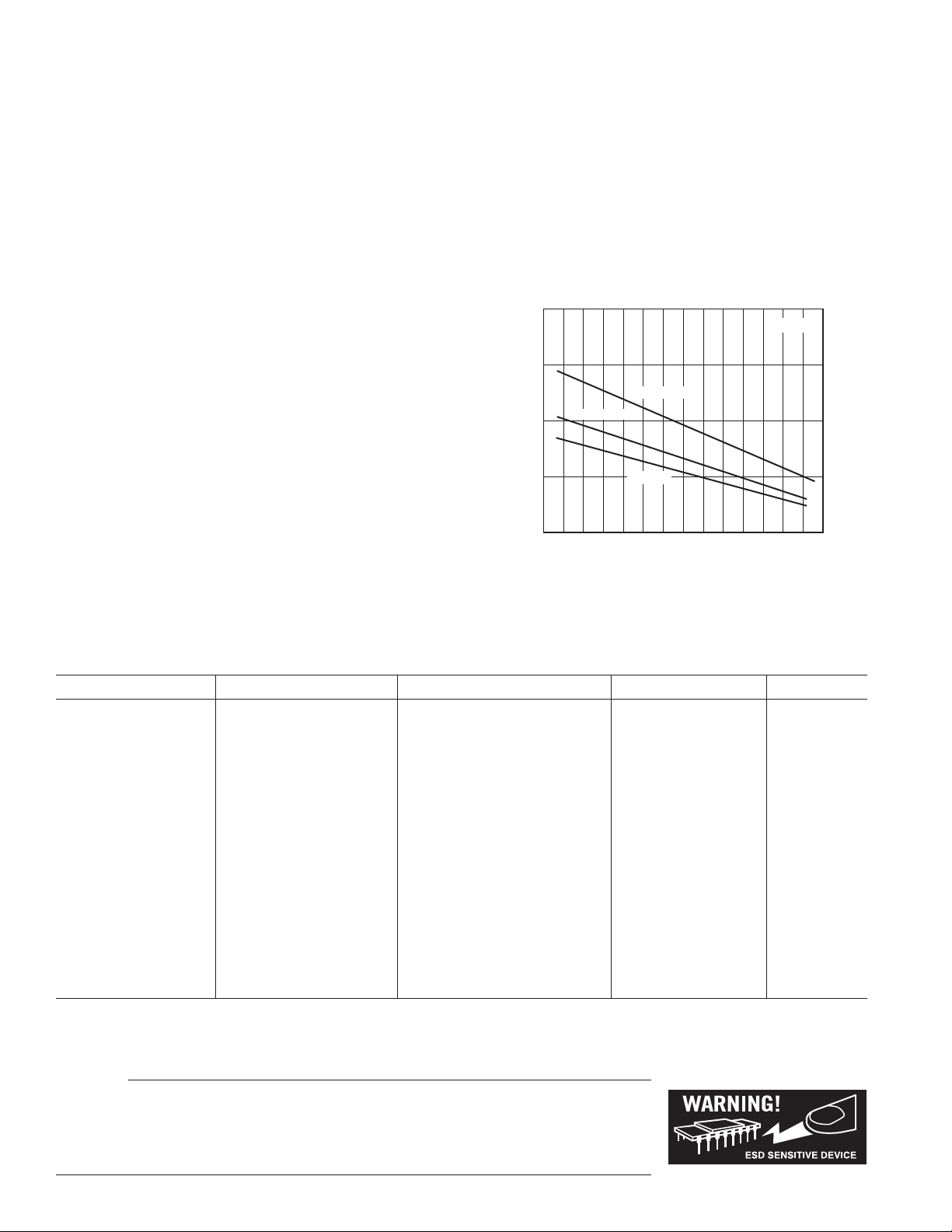
To ensure proper operation, it is necessary to observe the maximum power derating curves.
2.0
1.5
8-LEAD SOIC
8-LEAD MSOP
1.0
0.5
MAXIMUM POWER DISSIPATION (W)
0
–50 80–40
–30 –20 –10010 20 30 40 50 60 70
SOT-23-5
AMBIENT TEMPERATURE (ⴗC)
TJ = 150ⴗC
90
Figure 2. Plot of Maximum Power Dissipation vs.
Temperature
ORDERING GUIDE
Model Temperature Range Package Description Package Option Branding
AD8057AR –40°C to +85°C 8-Lead Narrow Body SOIC R-8 Standard
AD8057ACHIPS –40°C to +85°CDie Waffle Pak N/A
AD8057AR-REEL –40°C to +85°C 8-Lead SOIC, 13" Reel R-8 Standard
AD8057AR-REEL7 –40°C to +85°C 8-Lead SOIC, 7" Reel R-8 Standard
AD8057ART-R2 –40°C to +85°C 5-Lead SOT-23 RT-5 H7A
AD8057ART-REEL –40°C to +85°C 5-Lead SOT-23, 13" Reel RT-5 H7A
AD8057ART-REEL7 –40°C to +85°C 5-Lead SOT-23, 7" Reel RT-5 H7A
AD8057ARTZ-REEL7* –40°C to +85°C 5-Lead SOT-23, 7" Reel RT-5 H7A
AD8058AR –40°C to +85°C 8-Lead Narrow Body SOIC R-8 Standard
AD8058ACHIPS –40°C to +85°CDie Waffle Pak N/A
AD8058AR-REEL –40°C to +85°C 8-Lead SOIC, 13" Reel R-8 Standard
AD8058AR-REEL7 –40°C to +85°C 8-Lead SOIC, 7" Reel R-8 Standard
AD8058ARZ-REEL7* –40°C to +85°C 8-Lead SOIC, 7" Reel R-8 Standard
AD8058ARM –40°C to +85°C 8-Lead MSOP RM-8 H8A
AD8058ARM-REEL –40°C to +85°C 8-Lead MSOP, 13" Reel RM-8 H8A
AD8058ARM-REEL7 –40°C to +85°C 8-Lead MSOP, 7" Reel RM-8 H8A
AD8058ARMZ-REEL7* –40°C to +85°C 8-Lead MSOP, 7" Reel RM-8 H8A
*Lead free
CAUTION
ESD (electrostatic discharge) sensitive device. Electrostatic charges as high as 4000 V readily
accumulate on the human body and test equipment and can discharge without detection. Although the
AD8057/AD8058 features proprietary ESD protection circuitry, permanent damage may occur on
devices subjected to high energy electrostatic discharges. Therefore, proper ESD precautions are
recommended to avoid performance degradation or loss of functionality.
REV. B–4–

4.5
–40 85–30 –20 –10 0 10 20 304050607080
TEMPERATURE (ⴗC)
0.0
–3.5
–5.0
VOLTS
–0.5
–3.0
–4.0
–4.5
–1.5
–2.5
–1.0
–2.0
–5V SWING RL = 150⍀
–2.5V SWING RL = 150⍀
–1.5V SWING RL = 150⍀
TEMPERATURE (ⴗC)
6
–2
–6
–40 –30
V
OS
(mV)
–20 –10
0
10 20 30 40 50 60 70 80
–4
2
0
4
VOS @ ⴞ5V
V
OS
@ ⴞ1.5V
TEMPERATURE (ⴗC)
3.5
1.5
0
–40 –30
A
VOL
(mV/V)
–20 –10
0
10 20 30 40 50 60 70 80
0.5
2.5
2.0
3.0
A
VOL
@ ⴞ2.5V
A
VOL
@ ⴞ5V
85
1.0
(+) OUTPUT
4.0
VOLTAGE
3.5
3.0
2.5
2.0
1.5
OUTPUT VOLTAGE (V)
1.0
0.5
0
10 100k100
ABS (–)
OUTPUT
LOAD RESISTANCE (⍀)
1k 10k
Typical Performance Characteristics–AD8057/AD8058
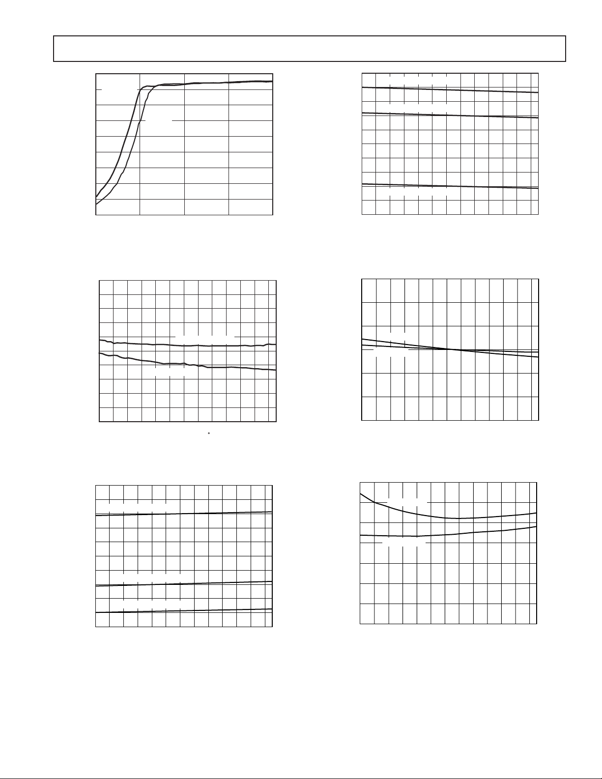
TPC 1. Output Swing vs. Load Resistance
–3.0
–3.5
–4.0
–4.5
–5.0
(mA)
–5.5
SUPPLY
–6.0
–I
–6.5
–7.0
–7.5
–8.0
–40 85–30 –20 –10 0 10 20 304050607080
TPC 2. –I
5.0
4.5
+5V SWING RL = 150⍀
4.0
3.5
3.0
2.5
VOLTS
2.0
1.5
1.0
REV. B
0.5
0.0
–4085–30
TPC 3. Positive Output Voltage Swing vs. Temperature
–I
SUPPLY
TEMPERATURE ( C)
SUPPLY
+2.5V SWING RL = 150⍀
+1.5V SWING RL = 150⍀
–20 –10
10 20 30 40 50 60 70 80
0
TEMPERATURE (ⴗC)
–I
@ ⴞ1.5V
SUPPLY
@ ⴞ5V
vs. Temperature
TPC 4. Negative Output Voltage Swing vs. Temperature
TPC 5. VOS vs. Temperature
TPC 6. Open-Loop Gain vs. Temperature
–5–
 Loading...